Note: Descriptions are shown in the official language in which they were submitted.
20~~~88
-1-
Power Amplifier for a Cellular Telephone
Field of the Invention
The present invention relates generally to mobile
radio communication systems which include cellular
telephones. More particularly, the invention relates to a
power amplifier for use with a cellular telephone that is
capable of operating in both analog and digital modes.
Background of the Invention
A cellular telephone system is a radio communication
system in which a plurality of mobile stations operate
within a cell which is serviced by a base station. There
are typically a relatively large number of cells and base
stations in a given service area. The base station in
each cell is connected to a message switching center which
in turn is connected to a public telephone system.
The first cellular mobile systems placed in public
use were analog systems typically used for speech or other
types of analog information. These systems include
multiple radio channels for transmitting analog
information between base and mobile stations by
transmitting analog modulated radio signals. The analog
systems are being replaced by dual mode systems which are
capable of operating in either a digital or analog mode of
operation. The Electronic Industry Association (EIA) has
published EIA/TIA Project No. 2398, entitled '°Cellular
System, Dual-Mode Mobile Station-Base Station
Compatibility Standard", IS-54 (Revision A), dated January
1991; and TR45.3, Project No. 2216, entitled "Cellular
System, Recommended Minimum Performance Standards for 800
MHz Dual Mode Mobile Stations," dated March 1991. These
Interim Standards provide specifications for the design of
a cellular telephone system which is capable of operating
in both analog and digital modes.
207~~88
-2-
The emerging mobile telephone system, which is
commonly referred to as the ADC-System, will work in both
analog and digital modes. A telephone operating in the
analog mode will have a power stage that will work
continuously at a power level determined by the base
station, and the modulation method will be FM. The
maximum allowed output power of a mobile station will
depend on the class of the mobile station. Presently,
there are four classes I, II, III and IV, and the maximum
output power of the classes are +6, +2, -2, and -2 dBW
ERP, respectively. Accordingly, such a system
advantageously employs a non-linear transmitter power
stage having a high power efficiency. The EIA has
specified that the digital mode will have a modulation
method which will include a substantial amplitude
variation in the transmitted signal (~/4-DQPSK). The
amplitude variation has an order of magnitude of
approximately 20dB, and the quotient between the peak and
average power is about 4dB. Accordingly, the power stage
for the digital mode will have to be linear, and it will
have to be dimensioned for a higher peak power. The
problem with a completely linear power stage is that the
power efficiency is relatively low. The specified digital
mode, however, only requires that the transmission take
place in one of three time slots in a full rate mode or in
one of six time slots in a half rate mode. Because the
transmission occurs in different time slots, the current
consumption is not of utmost importance.
It is desirable that the transmitter power amplifier
of a telephone in the ADC-system be able to operate (1)
continuously in the analog mode with high power
efficiency, and (2) in the digital mode where there are
restrictive requirements on power level and linearity.
Accordingly, there is a need for a transmitter power
amplifier that can efficiently meet the requirements of
207588
-3-
analog and digital operation in an ADC-system.
Summary of the Invention
The present invention relates to a transmitter power
amplifier for a cellular telephone that is capable of
operating in both analog and digital modes. The power
amplifier includes a linear power stage and a non-linear
power stage. The linear and non-linear power stages are
controlled by a switching means such that the non-linear
stage or the non-linear stage serially connected to the
linear stage are utilized during a particular mode of
operation. In the analog mode of operation, only the non-
linear power stage is used to amplify RF signals. In the
digital mode of operation only the non-linear stage in its
linear range of operation is used to amplify RF signals,
when the base station dictates a relatively low power
output. When the base station dictates a relatively high
level power output in the digital mode, both the linear
and non-linear power stages are used to amplify the RF
signals, where the non-linear stage acts as a linear
driver stage. The switching means which controls the
selection of the linear and non-linear power stages may
itself be controlled by a suitably programmed
microprocessor.
Brief Description of the Drawings
Fig. 1 is a block diagram which illustrates the power
amplifier of the present invention;
Fig. 2 is a schematic diagram of the switching means
used to control the non-linear power stage and the linear
power stages and
Fig. 3 is a flow chart of a software program tizat can
be utilized to control the switching means.
20~5~88
_4-
Detailed Description of the Invention
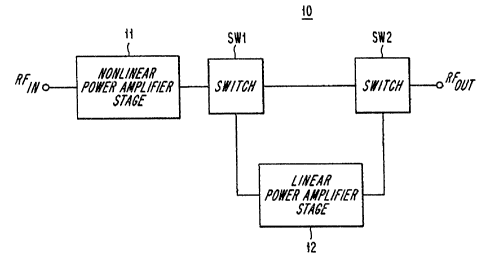
Referring to Fig. 1, a block diagram illustrates the
power amplifier 10 of the present invention. The power
amplifier 10 is used in the transmitter portion of a
cellular telephone that is capable of operating in both
digital and analog modes. The power amplifier 10 receives
an RF input signal at a terminal designated RF~~. The RF~~
signal is applied to a non-linear power amplifier stage
11. The output of the non-linear power stage 11 is
applied to a switching means comprised of switches SWl and
SW2. The output of switch SW2 is an RF output signal
which appears at a terminal designated RFa~t. In the
analog mode of operation only the non-linear power
amplifier stage 11 is used to amplify the RF input signal.
In the digital mode of operation at relatively high power
levels, the switching means causes the output of the non-
linear power amplifier stage 11 to be applied to the
serially connected linear power amplifier stage 12. The
output of the linear power amplifier stage 12 is then
applied back through the switching means and appears as
the RF output signal at the terminal RFo~t.
The present invention is based on the concept that
the non-linear power stage 11, when operated at a
relatively low power level, in relation to its maximum
power level, is sufficiently linear to meet the
requirements of the EIA Interim Standards for both analog 'a
and digital modes of operations. In other wards, the non-
linear power stage 11 is sufficiently linear to provide
modulation accuracy and adjacent channel emission even
when it is used at relatively low power levels in the
digital mode. In the analog mode of operation, the non-
linear power amplifier stage 11 alone is acceptable for
supplying all output power at all power levels. When
operating in the digital mode of operation and at a
207~~88
-5-
relatively high level power, the additional linear power
amplifier stage 12 is connected to the output of the non-
linear power stage in order to provide a RFout signal that
meets the linearity and power level requirements of the
digital mode.
Referring now to Fig. 2, a schematic diagram
illustrates the switching means which controls the non-
linear power amplifier stage 11 and the linear power
amplifier stage 12. Preferably, the additional linear
power amplifier stage 12 is comprised of one or more
transistor devices, either bi-polar or FET (field effect
transistor), having both collector/drain current and
base/gate voltages. Preferably, the switching means is
comprised of diodes D1 - D4: transmission lines TL1, TL2;
and capacitors 15, 16, 17.
In operation, a terminal 14 is connected to the
internal DC-feed, e.g., the battery voltage, of the power
amplifier 10, and it is connected to a collector or a
drain of the linear power amplifier stage 22. There is no
current flowing through terminal 14 until the transistor
devices of the linear power amplifier stage 12 are biased.
The diodes D3, D4 are, therefore, switched off. A
terminal 13 is either connected to ground when the linear
power amplifier stage 12 is switched off, or the terminal
13 is connected to a suitable voltage source when the
additional linear power stage 12 is activated. If GaAs
transistors are being used in the linear amplifier stage
12, voltages below ground may be needed to turn the device
off. If the terminal 13 is connected to ground, no
current flows through the diodes D1, D2, and the diodes
appear as an RF open circuit. Accordingly, an RF signal
applied to the non-linear power amplifier stage 1l is
transmitted through the transmission line TL1, the
capacitor 16, and the transmission line TL2 to the output
terminal RFout, when the terminal 13 is connected to
2075588
-6-
ground.
If the terminal 13 is connected to a suitable
voltage, a current flows through the diodes D1, D2 and
through the biasing circuit of the linear power amplifier
stage 12. The current flowing through the diodes D1, D2
makes them appear as an RF short circuit. Since the
linear power amplifier stage 12 is being biased, the
collector/drain currents also start to flow through the
diodes D3, D4, and the diodes appear as RF short circuits.
Accordingly, the RF~~ signal is transmitted through the
non-linear amplifier stage 11 and the linear power
amplifier stage 12 to the output terminal RFo~t.
The transmission lines TL1, TL2 are preferably two
quarter wavelength transmission lines. The switching
means also preferably includes decoupling capacitors 15,
17 and a capacitor 16 disposed between the transmission
lines TL1, TL2. The capacitor 16 presents a very low
impedance at RF frequencies, and acts as a DC-block. When
the diodes Dl, D2, D3, D4 have current flowing in them and
appear as an RF short circuit, the transmission line TL1
is shorted to RF g.round via the capacitor 15. Since the
transmission line TL1 is a quarter wavelength long, the
input terminal 18 of transmission line TL1 appears as an
open circuit at RF frequencies. Likewise, the input
terminal 19 of transmission line TL2 becomes RF shorted,
and the output terminal 20 of transmission line TL2
appears as an RF open circuit. This arrangement permits
the transmission of RF power from the non-linear power
amplifier stage 11 to the input terminal 21 of the
additional power amplifier stage 12, and the amplified RF
power is then transmitted from the output terminal 22 to
the RF output terminal.
The transmission lines TL1, TL2 have a length which
is related to the wavelength of the transmitted signal at
the center frequency of the band to which the transmitter
20'~~~88
is tuned. Accordingly, the physical length of the
transmission lines vary due to the material properties
from which the transmission lines are made.
Referring now to Fig. 3, there is a flow chart of a
software subroutine which can be used to control the
switching means. Preferably, the switching means is
controlled by a suitably programmed microprocessor running
the subroutine which has a starting step 31. In step 32 a
determination is made whether there is a command to end
transmission. If there has been a command to end
transmission then step 34 is performed removing current
from the diodes. If there has been no command, then it
means that the subroutine has been called, because the
telephone is being commanded to transmit or a power level
change is being commanded. The subroutine then advances
to step 33 where a determination is made whether the
telephone is operating in the digital made. If the
telephone is not operating in the digital mode, then it is
operating in the analog mode, and step 34 causes current
to be removed from the diodes. The current is removed
from the diodes when no voltage agpears at terminal 13.
Accordingly, RF signals are input to the non-linear power
stage 11 and transmitted to the RFo~t terminal through
transmission lines TL1, TL2 and capacitor 16.
If the telephone is operating in the digital mode, a
determination is made in step 35 whether the linear power
amplifier stage 12 is necessary. The linear power
amplifier stage 12 is necessary, if there is a requirement
for a relatively high power level. If the linear power
amplifier stage 12 is not necessary, then the software
insures that the current is not present at terminal 13 by
performing the step 34. If the linear power stage is
necessary, step 36 is performed which includes applying
current to the diodes D1-D4. If the diodes Dl - D4 become
conductive, then the linear power amplifier stage 12 is
2075588
_8_
coupled to the output of the non-linear power amplifier
stage 11. The subroutine then advances to an end step 37.
While the invention has been described in its
preferred embodiments, it is to be understood that the
words that have been used are words of description rather
than limitation and that changes within the purview of the
appended claims may be made without departing from the
true scope and spirit of the invention in its broader
aspects.