Note: Descriptions are shown in the official language in which they were submitted.
207~
SEI 92-20
1 Title of the Invention
SEMICONDUCTOR CHIP MODULE AND METHOD ~OR
MANUFACTURIN~ THE SAME
Back~round of the In ntio
(Field of the Invention)
The present invention relates to a semiconductor
chip module such as multi-chip module and single chip
module applicable for the fields of computers and
communications the like where high speed signal
processing is required.
(Related Background Art)
With the increased demand for large-scale function
and high speed operation of electronic devices, logic
LSIs have achieved high speed operation, with a delay
time per gate of several hundreds picosecond. HoweYer,
the conventional assembling structure which mounts a
large number of dual-in packages(DIPs) or plug-in
packages on a printed circuit board has become
difficult to bring out performance of high speed LSIs
sufficiently. In order to overcome such a problem, a
multi-chip module system has been developed and put
into practical use, which mounts large number of chips
on a single ceramic substrate and can provide high
speed per~ormance with high density assembling~refer to
- : . . ;~
207~93
SEI 92-20
1 "LSI HANDsooK"~ the first edition, pp.415-416, The
Institute of Electronics and Communi.cation Englneers of
Japan, 1984).
In the conventional t~pe of multi-chip module
system which mounts semiconductor chips with face up
bonding method and dissipates the heat generated by
semiconductor chips toward the substrate side, the heat
dissipation has been preventing the performance of the
semiconductor chip module from becoming aggravated due
to the heat resistance.
It was, however, not possible to obtain adequate
heat dissipation by this system. Accordingly, the
performance of the semiconductor chip module gradually
becomes aggravated, the rate of failure is increased,
and it becomes impossible to use the semiconductor chip
module over a long term.
Summary of the Invention
An obiect of the present invention is to provide a
semiconductor chip module capable of satisfactory
design for adequate dissipation of heat without
aggravation of the performance.
The semiconductor chip module according to a firs~
aspect of the present invention comprises a
semiconductor substrate on which a wiring por-tion is
,
.
207~9~
SEI 92-20
1 ~ormed, a semiconductor chip mounted so as to -~ace a
circuit side up to the wiring portion, a heat sink with
one end thereof contacted to the central portion of an
upper surface of the semiconductor chip; and a cap
which has an opening Eor exposing the other end of the
heat sink to the outside thereof, the cap enclosing the
semiconductor chips.
According to the semiconductor chip module of the
first aspect of the present invention, the heat
generated from tha semiconductor chip of face-up type
is conducted from the one end of the heat sink
contacted with the upper surface oE the semiconductor
chip to the other end thereof. This heat conduction
results in that the heat is introduced outside the cap
and then dissipated. Furthermore, there is no drawback
of short circuiting bstween pads in the cause of the
heat sink because the heat sink is mounted so as to
contact with the central portion of the face-up sur-Eace
of the semiconductor chip to avoid a contact with pads
arranged on the peripheral portion of the semiconductor
chip.
The semiconductor chip module according to a
second aspect of the present invention comprises a
semiconductor substrate on which a wiring portion is
formed; a semiconductor chip mounted so as to face a
2D75~93
SEI 92-20
1 circuit side up to the wiring portion; a heat sink wikh
one end thereo-f contacted to -the central portion of an
upper surface of the semiconductor chip; a cap ~hich
has an opening for exposing the other end o~ the heat
sink to the outside thereof t the cap enclosing the
semiconductor chips, and an insulating material which
coats a bonding wire for connecting the semiconductor
substrate and the semiconductor chip.
According to the semiconductor chip module of the
second aspect of the present invention, the heat
generated from the semiconductor chip o~ face-up type
is conducted from the one end of a heat sink contacted
with the upper surface of the semiconductor chip to the
other end thereof. This heat conduction results in
heat being introduced outside the cap and then
dissipated.
Further, a bonding wire connecting a semiconductor
substrate and semiconductor chips mounted thereon is
coated with insulating material. Therefore, evcn
though a heat sink is made of conductive material,
there is no aggravation in electric performance due to
short circuiting between the heat sink and the bonding
wire~ thus, it is possible to apply a large si~e of
the heat sink.
The semiconductor chip module according to a third
.
~7~3
SEI 92-20
1 aspect of the present invention comprises a
semiconductor substrate on which a wiring portion is
formed; a semiconduc~or chip mounted so as to face a
circuit side up to the wiring portion; a heat sink with
one end thereoE contacted to the central portion of an
upper surface of the semiconductor chip; a cap which
has an opening for exposing the other end of the heat
sink to the outside thereof, the cap enclosing the
semiconductor chips, and an insulating thermal compound
material placed on almost whole surface of the
semiconductor chip so as to contact both said one end
of the heat sink and the surface of the semiconductor
chip.
According to the semiconductor chip module of the
third aspect of the present invention, the heat
generated from the semiconductor chip of face-up type
is conducted from the one end of the heat sink
contacted with the upper surfaca of the semiconductor
chip to the other end thereof. This heat conduction
results in heat being introduced outside the cap and
then dissipated.
Especially, a insulating thermal compound material
is placed on almos-t whole surface of semiconductor
chip, heat produced from the peripheral portion of the
semiconductor chip which has I/0 circuit, etc. causing
- : .: - :
- , .
207~593
SEI 92-20
1 relatively a great amount of heat, can be conducted to
the heat sink through the thermal compound ma-terial.
The present invention will become more fully
understood from the detailed dcscription given
hereinbelow and the accompanying drawings which are
given by way of illustration only, and thus are not to
be considered as limiting the present invention.
Further scope of applicability of the present
invention will become apparent from the detailed
description given hereinafter. However, it should be
understood that the detailed description and specific
examples, while indicating preferred embodiments of the
invention, are given by way of illustration only, since
various changes and modifications within the spirit and
scope of the invention will become apparent to those
skilled in the art form this detailed description.
Brief DescriPtion of the Drawin~s
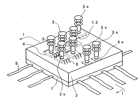
Fig. l is a perspective view showing an appearance
of a multi-chip module according to the present
invention,
Fig.2 is a cross sectional vertical view showing a
multi-chip module taken along the vertical direction of
a heat sink,
Fig. 3 is an enlarged plan view showing a
. .
~. '. ~A
207~93
SEI 92-20
1 semiconductor chip which can be used for a multi-chip
module according to the first embodiment of the present
invention,
Fig.4A is an enlarged side view showing a mounting
structure of the heat sink which can be used for a
multi-chip module according to the second embodiment of
the present invention,
Fig. 4B is an enlarged cross sectional view
showing a bonding wire taken along the plane II-II' of
Fig. 4A,
Fig.5 is an enlarged cross sectional vertical view
showing a mounting structure of the heat sink which can
be used for a multi-chip module according to the third
embodiment of the present invention.
- DescriPtion of the Preferred Embodiment
First of all, a basic structure of the
semiconductor chip module according to the present
invention is explained in reference with Fig. l and
Fig. 2.
The lower substrate l is made of aluminum oxide
material, for example, and has plural lead pins 5
extending from the side surface thereof. The lead pins
5 are connected to an electric wiring formed on the
upper substrate 6. The upper substrate 6 is made of
-,
- . -
2~7~593
SEI 92-20
1 insulating material of low dielectric constant. For
example, a polyimide multi-layered wiring structure
having three inches square size, a thermal resistance
of 3 C/W with a thermal via may be used(re~er to
"Copper Polyimide Multi-layered Wiring Boards",
HYBRIDS, Vol.7, No.1, pp.lO-12).
The lower substrate l is formed o~ a plate larger
than the upper substrate 6, and the upper substrate 6
is piled securely on the upper surface thereof. The
fringe of the cap 2 covers the upper surface o~ the
lower substrate l which is not covered by the upper
substrate 6. For that reason, the upper substrate 6 is
enclosed with the cap 2 and the lower substrate l. The
upper substrate 6 has electrodes exposed on the surface
thereof and ~ace-up type semiconductor chips 4 and
face-down type of semiconductor chips 4a connected to
the electrodes are mount d thereon as shown in the
figure. The face-up type semiconductor chips 4, as
indicated by its literal name, have a circuit side up.
A wirlng portion o~ the upper substrate 6 is connected
to the face-up type semiconductor chips 4 electrically
by wire bonding method. And the ~ace-down type
semiconductor chips 4a have a clrcuit side down so as
- to connect with wiring portion o~ the upper substrate 6
electrically by die bonding method.
- : : - :. .. ;:. , , ~ : . -
207~93
SEI 92-20
1 Also, the cap 2, for example, is Yormed of l mm
thick Kovar in a shape o~ a lid. An opening 2a wikh an
inner diameter of 30 to 50 ~m is formed in the cap 2 at
the position corresponding to the mounting position oP
the face-up type semiconductor chip 4 or the face-down
type semiconductor chip ~a. One end of the heat sink
3, 3a, 13 is inserted into the opening 2a. For the
material of cap 2, metal such as aluminum, copper
tungsten alloy, etc., or ceramics such as AlN, SiC can
be used.
The heat sink 3, 3a, 13 mentioned above are made
of material of high heat conductivity such as Al and
CuW and includes an insertion portion and a heat
dissipation portion. The insertion portion has a shape
which allows to be easily inserted into above mentioned
opening 2a, for example, a rod shape. And the heat
dissipation portion has a structure with a large
surface area to get easily cooled by natural cooling,
for example, formed in a disc shape. As the number of
stages of dissipation portion is increased, the speed
of cooling is generally increased. For that reason,
the insertion of the heat slnk 3, 3a, 13 into the
interior of the cap ~ is simp~le and the heat generated
from the face-up type semiconductor chips 4 can be
dissipated to the outside of the cap 2 effectively. It
~07~3
SEI 92-20
1 is preferable in order to conduct the heat effectively
from the face-up type semiconductor chip 4 to ~he heat
sink 3, 13 that the con-tacting st~te between h0at sink
3, 13 and the surface of the semiconductor chip ~ is
surface contact. Accordingly, the tip end of the
insertion portion of the heat sink 3, 13 is preferably
flat in case that the upper surface of the
semiconductor chip 4 is flat.
Where the material of the heat sink 3 is
conductive material such as Al or CuW, the tip area of
heat sink 3 must be relatively small to avoi.d short
circuiting between the bonding wire and TAB pads. If
it is, however, insulating material such as AlN or
cubic phase boron nitride(CBN), etc., the degree of
over design and freedom becomes high since the contact
with bonding wire does not cause a serious problem.
Moreover, the outside diameter of the heat sink is
basically determined according to the heat generation
area of the-semiconductor chip. For example, in the
case that 10 mm square IC chip which generates heat
from the whole upper surface thereof, a heat sink
having 10 mm diameter may be preferably used. If the
heat generation area is a part of the upper surface of
the semiconductor chip, a heat sink having a diameter
to cover the area may be used. Further, the si~e of
:, .- :: : : :: : ;: :. . . .
~Q7~3
. SEI 92-20
1 the opening 2a of the cap 2 is preferably larger -than
the heat sink 3, 3a, 13 to be inserked therein by 0.05
mm where the material of the cap 2 is metal and 0.1 mm
where the material of the cap 2 is ceramics,
Next, mounting structure of the heat sink
applicable for a multi-chip module according to the
first embodiment of the present invention is explained.
Fig. 3 is a top view showing a face-up type
semiconductor chip 4 mounted on the semiconductor chip
module according to the first embodiment. *he
peripheral portion of this semiconductor chip 4 has
pads 7 along the dotted line in the figure, the heat
sink 3 is arranged on the central portion of the
semiconductor chip 4.
In this case, as it is possible to have the pad 7
with the size of 80 ~m if Au wire of 2~ ~m is used for
the bonding wire 8l it becomes possible to contact the
heat sink 3 with the semiconductor chip 4 except the
narrow area covering 130 ~m for one side of the
semiconductor chip 4 and the total area of 260 ~m for
both sides where the pads 7 are arranged only on the
peripheral portion thereof and the distance between the
pad end and the chip end is ~0 ~m. The thermal
resistance can be lowered from 10 C/W to about ~ C/W
for this structure.
2a7~3
SEI 92-20
1 Further, the surface of the face-up type
semiconductor chip 4 except the area where pads 7 are
formed is protected with a passivation ~ilm such as SiN
or SiON. Accordingly, there is no drawback even if
heat sink 3 is contacted with the circuik side of the
semiconductor chip.
The multi-chip module according to the first
embodiment is packaged with the steps of: enclosing a
top surface of the upper substrate 6 fixed on the lower
subs-trate 1 with a cap 2; inserting one end of heat
sink 3 into a opening 2a of the cap 2 to contact the
tip end thereof with an upper surface of semiconductor
chip 4; and fixing the heat sink 3 with the cap 2 by
putting solder into the gap between the opening 2a of
cap 2 and the heat sink 3 while the heat slnk 3 is in
contact with the semiconductor chip 4, for example.
Also, all semiconductor chips have heat sink 3
thereon in this embodiment, but the heat sink 3 may be
selectively applied to the semiconductor chips 4 which
produce a large amount of heat. As stated above, one
heat sink 3 is applied ~or one semiconductor chip 4, it
is assured that a heat sink 3 is mounted on a
semiconductor chips 4 even though plural semiconductor
chips are mounted on the substrate surface with
different height from the substrate surface.
12
.:. : : .,
2~7~593
SEI 92-20
1 As the multi-chip module of the first embodiment
has the structure described above, the heat sink 3 is
mounted on each of the semiconductor chips 4. For that
reason, it is possible to design a semiconductor
structure in dissipation well and there is no
inconvenience for designing a semiconductor chip module
which can operate with high speed. Also, it is
possible to lower the heat resistance of face-up type
semiconductor chip 4. Further, as one heat sink 3 can
be mounted selectively on one semiconductor chip 4,
heat resistance can be reduced even in the case of
multi-chip module having face-up type semiconductor
chip 4 and face-down type semiconductor chip 4a.
Next, a multi-chip module according to the second
embodiment of the present invention is explained in
reference with Figs. 1, 2, 4A and 4B. This multi-chip
module is different from the embodiment described above
since this multi-chip module uses a heat sink made of
conductive material, a wire made of conductive material
being coated with insulating material.
In general, a conductive heat sink has better heat
conductivity and dissipation efflciency rather than a
insulating heat sink. Considerlng this point~ it is
preferable to use a conductive heat sink. Also, the
dissipation efficiency increases as the size of the
13
2~75~93
SEI 92-20
1 heat sink become larger.
It, however, arises an anxiety that the electric
characteristics become aggra~ated due to a contact with
the bonding wire 8 in case that a large heat sink is
used. Therefore, the embodiment uses the bonding wire
8 coated with insulating material 8b such as urethane
of 0.5 to 0.7 ~m thickness, etc. so as to allow the use
of conductive heat sink 13 in large size. Because of
this, the conductive heat sink 13 may contact wlth the
bonding wire 8 and the heat sink 13 may be in a large
size. These result in the improvement of dissipation
for- semiconductor chip module.
Further, the circuit surface of the semiconductor
chips 4 is protected with a passivation film such as
SiN or SiON. Accordingly, there is no drawback even if
heat sink 13 is contacted with the circuit side of the
semiconductor chip 4.
The detail is explained in reference with Figs. 4A
and 4B. As the bonding wire 8 is coated with
insulating material 8b (See Fig. 4B), it allows that
the gap "t" between the heat sink 13 and the bonding
wire 8 can be decreased to the contacting state of
them. Therefore, the heat sink 13 can be in a large
size.
Also, as there is no bad effect in electrical
14
2~7~9~
SEI 92-20
1 characteristics where the heat sink 13 is contacted
with bonding wire 8 more or less, ik is possible to
manufacture the parts in reduced equi.pment tolerance
and production tolerance, thus, the yield is impro~ed.
Further, the cost o~ materials may be lowered
since conductive material such as A1 and CuW, etc.,
being cheaper than insulating material such as AlN,
cubic phase boron nitride, diamond, etc., can be used.
Moreover, it is necessary to pay attention not to
decline the mechanlca]. reliability while it does not
matter whether or not the heat sink 13 may be
contacted electrically with the bonding wire 8 more or
less~
The multl-chip module according to the second
embodiment i6 packaged with the steps of: enclosing a
top surface of the upper substrate 6 ha~ing the face-up
type semiconductor chip 4 and the face-down type
semiconductor chip 4a thereon and ~ixed on the lower
substrate 1 with a cap 2; inserting one end o~ heat
sinks 3, 3a' 13 into a openings 2, 2a to contact the
tip end thereof with the upper surface o~ semlconductor
chip 4, 4a; and ~ixing the heat sinks 3, 3a, 13 on the
cap 2 by putting solder into the gap between the
openings 2, 2a of cap 2 and the heat sinks 3, 3a, 13
whiIe the heat sinks 3, 3a, 13 are in contact with the
1~
- : ,.- : -: ~ ~ -: :: .:: :., ., . , :
.
2075~3
SEI 92-20
1 semiconductor chip 4, 4a, for example.
Next, a multi-chip module according -to ~he third
embodiment of the present invention is explained in
reference with Fig. 1, 2 and 5. This multi-chip module
is dif~erent from the above mentioned embodiments since
this multi-chip module has an insulating thermal
compound material placed on almost whole surface of
semiconductor chips.
Also a thermal compound material is placed on
almost whole surface of each of the face-up type
semiconductor chip 4. It is for improving the
dissipation o~ heat. As it is desired to avoid the
contact between the bonding wire 8 and the heat sink 3
as much as possible, the heat sink 3 should not be
contacted with the semiconductor chip 4 except the
central portion thereo~.
Accordingly, the heat dissipated outside is mainly
the heat generated from the central portion o~ the
semiconductor chip 4 with which the heat sink 3
contacts. And the heat generated from the peripheral
portion of the I/0 circuit of the semiconductor chip 4
is not sufficiently absorbed by the heat sink, but is
dissipated to the substrate side.
It is important to dissipate the heat generated
from the I/0 circuit portion through the heat sink
16
,- : ,,
, . ,- . . ~,. ~ . ,
2~7~93
SEI 92-20
1 effectively because the peripheral portion oP the I/0
circuit generates a great amount of heat in general.
If insulating thermal compound material is placed on
almost whole area o~ the face--up type semiconductor
chip like the present embodiment(Fig. 5), the heat frorn
not only the central portion of the semiconductor chip
but the peripheral I/0 circuit portion thereof can be
conducted to the heat sink 3. As the thermal compound
material 1 is insulating, there is no problem in
performance of the semiconductor chip 4 even if the
thermal compound material 1 is placed on whole area of
the semiconductor chip 4 and contacts wi-th the bonding
wire 8. The insulating thermal compound material 1 may
be made of epoxy resin contained a great amount of e.g.
finely powdered diamond or cubic phase boron
nitride(CBN).
From the invention thus described, it will be
obvious that the invention may be varied in many ways.
Such variations are not to be regarded as a departure
2 from the spirit and scope of the invention, and all
such modifications as would be obvious to one skilled
in the art are intended to be included within the scope
of the following claims.