Note: Descriptions are shown in the official language in which they were submitted.
207585 5
-1-
SCANNING MICROSCOPE COMPRISING FORCE-SENSING MEANS
Field of the Invention
The invention relates to the field of scanning microscopes, and more
particularly to those microscopes that employ a fine probe which senses forces
close
to the surface of the object which is being scanned.
_Art Background
In recent years, scanning microscopes based on optical, electrical, or
atomic force sensing have proven to be useful in a variety of disciplines. For
example, the use of such microscopes is a useful adjunct to scanning electron
microscopy (SEM) because contrast mechanisms alternative to those of SEM may
be
employed to explore the topography and composition of surfaces.
Atomic force microscopes have been described, in which a sharply
pointed probe tip is brought near the surface of a sample, and forces acting
normal to
the surface affect the motion of the tip. For example, U.S. Patent No. Re.
33,387,
issued to G.K. Binnig on Oct. 16, 1990, describes such an arrangement where
the tip
is mounted on a cantilever beam which is deflected as a result of the normal
forces.
A further example is U.S. Patent No. 4,851,671, issued to D.W. Pohl on
July 25, 1989, which describes an alternative arrangement in which the tip is
mounted on an oscillating crystal, and the frequency of oscillation is altered
by the
presence of normal forces.
When there is relative, lateral motion between the probe tip and the
sample surface, forces are also present which act parallel, rather than
normal, to the
surface. (By "lateral" is meant that the relative displacement has a component
which
is, on the average, parallel to the sample surface in the vicinity of the
probe.) Such
shear forces may arise, for example, from static or dynamic friction between
the tip
and the sample. Other shear forces arise as viscous forces in the air or other
fluid
medium between the tip and the sample.
A probe which senses shear forces can offer some advantages over
conventional, normal-force-sensing probes. For example, shear forces generally
act
over greater distances, measured from the sample surface, than do normal
forces.
The farther from the surface a probe can act, the smaller is the likelihood of
damaging the probe or the sample. Acting at a greater distance also makes it
possible to scan more quickly, because collisions with high surface features
are more
easily avoided. Furthermore, a cantilever-mounted normal-force probe generally
2075855
-2-
needs to be rather stiff along the lateral direction. By contrast, a shear-
force probe can
be much more flexible along that direction, reducing the likelihood of damage
by lateral
collisions with the walls of surface features on the sample.
A probe which, in a limited context, senses forces which are directed
parallel to a sample surface has been described in U.S. Patent No. 4,992,659,
issued to
D. W. Abraham, et al., on Feb.12, 1991. That patent describes a scanning,
tunneling
microscope which has a probe adapted to detect magnetic fields in the sample
being
scanned. Magnetic fields in the sample act on the tunnel current in the probe
to cause a
Lorentz-force deflection of the probe parallel to the sample surface. Such a
probe is
limited in use to metallic samples having magnetic properties, and is subject
to the
same dangers of probe or sample damage as are conventional, normal-force-
sensing
probes.
Despite its advantages, practitioners in the field have hitherto failed to
provide a general-purpose shear-force-sensing probe.
Summary of the Invention
We have invented a scanning, imaging system which includes a shear-
force-sensing probe which is to be used for scanning at least a portion of the
surface of
a sample. Thus, the inventive system includes a fine probe which has a
longitudinal axis
and a tip. The system also includes means for positioning the probe tip
adjacent the
surface, and means for displacing the probe tip relative to the surface. The
relative tip
displacement includes a scan pattern, such as a raster scan, which lies
substantially in a
plane, referred to hereinafter as the "scanning plane." The scanning plane
lies
substantially parallel to the surface portion which is scanned. The
displacement means
also include means for oscillating the probe tip relative to the surface at
least at one
oscillation frequency. In contrast to prior art scanning systems in which a
probe tip is
oscillated, the relative tip oscillations according to the inventive system
lie substantially
within the scanning plane. The system further includes a position-sensitive
photodetector, and means for optically imaging the probe tip onto the position-
sensitive
photodetector such that changes in the oscillation of the probe tip can be
detected.
In accordance with one aspect of the present invention there is provided
a system for scanning at least a portion of the surface of a sample, the
system
comprising: a probe having a longitudinal axis and a tip; means for
positioning the
probe tip adjacent the surface; means for displacing the probe tip relative to
the surface
such that a scan pattern is described in a plane, to be referred to as the
"scanning
~~075855
-2a-
plane," which lies substantially parallel to the surface portion; and means
for oscillating
the probe tip relative to the surface at least at one oscillation frequency,
characterized in
that the oscillating means are adapted to oscillate the probe tip
substantially within the
scanning plane; and the system further comprises: a position-sensitive
photodetector;
and means for optically imaging the probe tip onto the position-sensitive
photodetector
such that changes in the oscillation of the probe tip can be detected.
In accordance with another aspect of the present invention there is
provided a method for manufacturing an article, comprising the steps of: a)
providing a
multiplicity of semiconductor bodies, each semiconductor body having a surface
to be
patterned; b) setting at least one process parameter; c) processing at least a
first
semiconductor body according to the process parameter such that a pattern is
formed on
the surface of the semiconductor body, the pattern having a characteristic
dimension; d)
measuring the characteristic dimension in the first semiconductor body; e)
comparing
the characteristic dimension to a predetermined range of values; f) if the
characteristic
dimension lies outside the predetermined range of values, changing the process
parameter to bring the characteristic dimension within the predetermined range
of
values; g) after (f), processing at least a second semiconductor body
according to the
process parameter; and h) performing, on at least the second semiconductor
body, at
least one additional step toward completion of the article, characterized in
that the
measuring step comprises situating, adjacent a portion of the surface, a probe
having a
tip; displacing the probe tip relative to the surface such that a scan pattern
is described
in a plane, to be referred to as the "scanning plane," which lies
substantially parallel to
the surface portion; oscillating the probe tip, relative to the surface, such
that the
oscillations lie substantially within the scanning plane; optically imaging
the probe tip
onto a position-sensitive photodetector which produces an output signal; and
processing
the output signal such that changes in the oscillation of the probe tip are
detected.
Brief Description of the Drawings
FIG. 1 is a schematic representation of an exemplary embodiment of the
inventive imaging system.
FIG. 2 is a schematic representation of an exemplary means for position-
sensitive photodetection.
207585 5
-3-
FIG. 3 is a schematic representation of an alternative means for
position-sensitive photodetection.
FIG. 4 is a schematic representation of a preferred method for aligning a
pinhole mask for purposes of position-sensitive photodetection.
FIG. 5 is a schematic representation of an optical arrangement for
external illumination of a probe tip, according to one embodiment of the
invention.
FIGS. 6 and 7 are schematic representations of exemplary probes useful
for near-field scanning optical microscopy as well as for shear-force
detection.
FIG. 8 is a schematic representation of an exemplary arrangement for
raster scanning and for oscillating the probe relative to the sample,
according to one
embodiment of the invention.
FIGS. 9-11 are schematic representations of alternative probe-tip
configurations.
FIG. 12 is a schematic representation of an exemplary optical
arrangement in the case where the probe tip is moved as part of the raster
scan.
FIG. 13 is a schematic representation of the inventive imaging system in
one embodiment, including an exemplary electronic signal-processing circuit.
FIG. 14 is an exemplary image produced by the imaging system of
FIG. 13.
Detailed Description
A currently preferred embodiment of the invention is now described
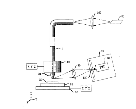
with reference to FIG. 1. A probe 10 is provided, together with stage 20 for
supporting sample 30, and means 40 and 50 for displacing the probe relative to
the
sample. The displacing means are exemplarily piezoelectric actuators capable
of
displacing the sample or the stage in at least one lateral direction (denoted
X and Y
in the figure), and/or in the vertical direction (denoted Z). Light source 60
is
provided for illuminating the probe tip 70, and position-sensitive
photodetector 80 is
provided for detecting light from the probe tip and sensing displacements of
the
probe tip.
Shear forces affect the motion of the probe tip, relative to the sample
surface, in several respects that make detection possible. For example, a
lateral,
periodic (e.g., sinusoidal) oscillation is readily imparted to the probe tip
by actuator
40. (Such oscillatory motion will be referred to hereafter as "dither"
motion.) In the
presence of shear forces, the amplitude of the oscillation is changed as the
tip is
brought closer to the sample surface. Additionally, the phase of the
oscillation,
relative to the driving voltage, is observed to change as the tip approaches
the
20 7 58 5 5
-4-
surface. Both amplitude changes and phase changes are readily observed. Either
type of change, or a combination of both, is useful for feedback and for
imaging.
The probe will generally have at least one mechanical resonance at a
resonance frequency. (Resonances of interest will be correspond to local
maxima in
the oscillatory amplitude, relative to variations of the driving frequency.)
The
resonant frequency will also be affected by shear forces. If the probe is
oscillated at
a frequency which is near resonance, shear forces will shift the resonance
either
closer to, or further from, the driving frequency. As a result, the
oscillatory
amplitude of the probe tip will increase or decrease, respectively. Both
amplitude
and phase are particularly sensitive to shear forces under such near-resonant
driving
conditions. This is especially true because probes are readily made having
high Q
(i.e., quality factor) values. Thus, for example, it may be advantageous to
drive the
probe oscillations at a near-resonant frequency. An appropriate frequency for
amplitude detection produces, e.g., an oscillatory amplitude which, when the
probe
tip is far from the sample surface, is about 70% of the (local maximum)
amplitude at
resonance, since that is where the slope of the~resonance curve is steepest.
On the
other hand, the phase is most sensitive to the driving frequency precisely at
resonance. Thus, a preferable frequency for phase detection is approximately
at
resonance.
The inventive technique is sensitive even to very small shear forces,
because, inter alia, the relevant spring constant of the probe tip is quite
small,
typically 0.1 - 1000 N/m, and the peak-to-peak displacement during an
oscillation is
typically only about 50 - 100 A when the probe tip is far from the sample
surface
(i.e., when shear forces are negligible), and generally even smaller when the
probe
tip is sensing the surface. An additional, desirable consequence of the low
spring
constant, high Q value, and small oscillatory displacement is that the
technique is
relatively non-destructive of the sample and probe tip.
In an exemplary detection scheme, tip 70 is optically imaged onto
position-sensitive detector 80 by, e.g., lens 90. Such a detector includes,
for example,
a pair of photodiodes arranged on either side of a gap. Such an arrangement of
diodes 100, 100' is shown in FIG. 2. (Alternatively, for two-dimensional
sensitivity,
four photodiodes 101 - 104 are readily provided in a quadrilateral arrangement
separated by a cross-shaped pair of gaps, as shown in FIG. 3.) An alternative
detector includes a photomultiplier tube 110 arranged to detect only such
light as
passes through a pinhole 120, as shown in FIG. 1. The tip is optically imaged
onto
the pinhole, except for a small lateral offset 130 in the direction of the
dither motion,
2075855
-5-
shown in FIG. 4. The amount of offset is adapted to maximize the ac component
(at
the dither frequency) of the photomultiplier output when the probe tip is
dithered at a
given dither amplitude. (It should be noted in this regard that the absolute
ac signal is
typically maximized, rather than the ac signal normalized to the corresponding
do
signal.) The image of the probe tip (shown in the figure as an intensity
profile) will
typically be a diffraction-limited spot magnified by the magnification of lens
90.
The pinhole diameter will typically be equal to the diameter of this
(magnified) spot.
The offset will typically be just enough to give about 70% of the maximum do
signal
from a stationary image.
One advantage of the inventive technique is that the displacement of the
probe tip is measured directly. As a consequence, systematic or slowly varying
errors in the position of the probe tip are readily detected and corrected.
Such errors
may arise, e.g., from non-linear behavior of the piezoelectric actuators, or
from
lateral attraction between the probe tip and a vertical wall of a nearby
surface feature
on the sample.
The light used for imaging the tip is readily impinged onto the tip from
an external source 140, as shown in FIG. 5. Alternatively, if the tip is
fashioned from
an optical fiber, as shown in FIG. l, means 150 are readily provided for
coupling the
light into the fiber at the end distal the probe tip, and light for imaging is
light
emitted by the tip. Such internal illumination, when it can be used,
represents a
significant advantage over other force microscopes using optical detection,
because
the light spot remains bound to the tip, and need not be realigned each time
the tip is
moved. However, internal illumination cannot be used, and external
illumination
must instead be used, where the probe is made from an opaque material, for
example
by electrochemically etching a tungsten wire.
Optical fiber probes are particularly useful in conjunction with near-field
scanning optical microscopy (NSOM). That is, the same probe can be used as
both a
shear-force probe and as an NSOM probe. In addition to providing a contrast
mechanism alternative to the optical NSOM contrast mechanism, the shear-force
mode of operation can provide a feedback signal for keeping the probe at an
approximately constant height above the sample during NSOM imaging. The use of
such feedback is advantageous because it improves NSOM image resolution and
contrast, and permits the probe to follow the vertical contours of the surface
being
scanned.
2075855 --
-6-
Optical fiber probes for NSOM are readily made from either single-
mode, or multimode, fiber. Single-mode fiber is preferred because it generally
provides better signal strength, reliability, and spatial resolution.
If an internally illuminated optical fiber probe is to be used, it is
generally preferable to use a fiber which does not have a metal coating,
because such
coatings tend to reduce the signal strength. However, there is an important
exception
to this rule. That is where the same fiber probe is to be used for both shear-
force
detection and for NSOM. It is advantageous, for purposes of NSOM imaging using
optical fiber probes, to coat at least a terminal portion of such probes with
metal, or,
more generally, with an opaque material having a relatively small penetration
depth
for the electromagnetic radiation guided in the fiber. Opaque coating 165 is
depicted
in FIGS. 6 and 7. In the case of an internally illuminated NSOM probe, it may
be
useful to employ the same light for NSOM imaging and shear-force detection,
despite the fact that a coated fiber is used.
In the case of combined NSOM and shear-force detection, using either
internal or external illumination, the do component of the detected light may
be used
to create an NSOM image, while the normalized ac component is used to create a
shear-force image, or to provide a shear-force feedback signal. (The
normalized ac
component is the absolute ac component, divided by the do component.
Normalization is necessary in order to compensate for variations in, e.g., the
transmissivity of the sample.) Alternatively, a beamsplitter may be employed
to
divert some of the light from the probe tip before it reaches the position-
sensitive
detector, and instead, to direct it into a separate photodetector for NSOM
imaging.
Such a scheme may improve the signal-to-noise ratio in the NSOM image by
reducing the effects of mechanical vibrations, which might otherwise add low-
frequency noise to the NSOM signal passed through the pinhole.
Although the same wavelength can be used for both NSOM imaging and
shear-force detection, it may be useful, especially where extremely high
sensitivity is
required, to employ separate wavelengths. In such a case, spectral filtering
would be
used to exclude the shear-force wavelength from an NSOM optical detector and
to
exclude the NSOM wavelength from a shear-force optical detector. In such an
arrangement, the shear-detection wavelength would come from an external light
source and would typically be focussed to a diffraction-limited spot on the
probe tip
by, e.g., a microscope objective.
20 7 58 5 5
7_
As noted, above, feedback by shear-force detection is useful in NSOM
in order to maintain the probe tip at a constant, or approximately or
inferentially
constant, distance from the sample surface. One convenient way to achieve this
is to
maintain a constant shear-force signal during an NSOM scan in which the same
probe is used both for NSOM imaging and for shear-force detection. Changes in
the
shear-force signal are used in a closed loop arrangement using the vertical
(i.e., Z-
component) displacement capability of actuator 40 or actuator 50 (shown in
FIG. 1)
to adjust the height of the tip above the sample in order to restore the
signal to a
predetermined level.
As illustrated in FIG. 8, the dither motion 160 used for shear-force
sensing is readily imposed on the raster motion 170 of the NSOM scan. Thus,
the
total relative motion between the probe tip and the sample is the sum of a
raster
component and a dither component. The relative motion may be provided entirely
by moving the sample, entirely by moving the probe, or by a combination of the
two.
The dither frequency should be high enough to provide an adequate signal-to-
noise
ratio in the NSOM image. For that purpose, it is often desirable to make the
dither
frequency greater than the pixel frequency of the NSOM scan.
For example, a useful raster pattern is readily generated by moving the
sample along the slow scan axis (driving waveform 180 of FIG. 8), and moving
the
probe along the fast scan axis (driving waveform 190). In such a case, the
position-
sensitive optical detector should be insensitive to probe displacements along
the fast
axis, and the dither motion should consequently be oriented parallel to the
slow scan
axis (driving waveform 200). Alternatively, it is simpler, but generally
slower, to
effectuate the raster motion by moving the sample along both the fast and slow
axes.
In such a case, by contrast, the dither motion (which is then necessarily
applied to
the probe) may take the fast-axis orientation, or the slow-axis orientation,
or even an
intermediate orientation.
A probe which is to be used for combined NSOM imaging and shear-
force imaging is preferably made from a tapered, optical fiber. As noted, it
is
desirable to provide an opaque coating on the outside of the fiber at least in
the taper
region, in order to confine the electromagnetic radiation propagating in the
fiber.
Such a coating should have a small penetration depth for electromagnetic
radiation
of the wavelength used for NSOM imaging. For visible wavelengths, aluminum
coatings are useful for this purpose. (Hereafter, the term "light" will be
used to
denote, not only visible wavelengths, but also infrared and ultraviolet
wavelengths of
electromagnetic radiation.) Appropriate NSOM probes, and methods of NSOM
2075855
_g_
imaging, are described in U.S. Patent No. 5,272,330, issued on Decembei 21,
1993.
With reference to FIGS. 6 and 7, the tapered end 210 of fiber 215
terminates in a substantially flat face 220 oriented substantially
perpendicularly to
the longitudinal axis of the fiber. An optical aperture 230 is defined in the
end flat in
one of two ways. In the first, shown in FIG. 6, the end flat is simply left
bare of the
opaque coating, so that substantially the entire area of the end flat can
admit
electromagnetic radiation to the fiber. In the second, shown in FIG. 7, the
opaque
coating is, in fact, applied to the end flat as well as to the sides of the
fiber probe. In
that case, an aperture, smaller than the end flat, is defined by excluding, or
by
removing, opaque coating material from a circular region at or near the center
of the
end flat.
If the probe is to be used for shear-force imaging without NSOM
imaging, it is not necessary to make the probe from an optical fiber. The only
requirements are a relevant spring constant less than about 1000 N/m, and the
ability
to form a probe tip fine enough to provide the desired spatial resolution.
Thus, as
noted, a useful probe is readily made from, e.g., an electrochemically etched
tungsten wire. However, it is preferable to use an optical fiber, and still
more
preferable to use a single-mode optical fiber, for several reasons. For
example,
probes made from optical fibers are simple and inexpensive, and can be made by
a
simple piocess which gives highly reproducible results. Fiber probes are
readily
drawn down to a very small tip diameter, for example, a single-mode fiber is
readily
°
drawn down to a tip as small as about 100 A in diameter. Furthermore, a taper
angle
(defined as one-half the vertex angle) as small as about 10°, or even
less is readily
produced near the tip of such a drawn fiber.
Furthermore, the drawing process that results in production of a fiber
probe is readily adaptable to produce extremely sharp tips for enhanced
resolution.
That is, tips are readily made which terminate in a nipple 240 (see FIG. 9) or
in an
end flat having a sharp edge 250 (see FIG. 10). A nipple-shaped tip is
particularly
useful because it combines two desirable properties. First, it can be made
very thin
in order to give high resolution and to penetrate narrow crevices in the
sample
surface. Second, it can be made relatively short, so that although it is thin,
it is still
stiff enough to oscillate at desirable frequencies.
If an end flat having a sharp edge is oriented perpendicular to the
longitudinal axis of the fiber (as is usually the case), the fiber must be
tilted in order
to expose the edge to the surface of the sample. However, a fiber probe having
a
2075855
-9-
"hook-shaped" tip 260, as shown in FIG. 11, is readily produced, in which a
terminal
portion of the probe is curved in order to expose the edge to the sample
surface even
when the rest of the probe is oriented perpendicular to the surface. It should
be
noted in this regard that if a fiber probe is to be used for shear-force
detection
without NSOM imaging, the opaque coating can be omitted without substantially
diminishing the effectiveness of the probe.
It should be further noted that although in a currently preferred
embodiment, the longitudinal axis of the probe is substantially perpendicular
to the
sample surface, such perpendicularity is not an essential requirement. As
noted, a
perpendicular probe is flexible in the lateral direction and thus
advantageously
avoids collision damage against vertical surface features. In some cases, it
may be
desirable to tilt the probe relative to the sample, in order to avoid damage
from
collisions in the vertical direction, or in order to bring the sharp edge of
an end flat
adjacent the sample surface without forming a hooked probe tip. For such
purposes,
the longitudinal axis of the probe may usefully describe an angle with the
sample
surface of about 45° to about 90°.
Various illumination geometries are useful for NSOM imaging. In an
illumination-transmission geometry, light is emitted by the probe and detected
after
transmission through the sample. In an illumination-reflection geometry, light
is
emitted by the probe and detected after reflection from the side of the sample
nearest
the probe. (In either case, the light which is detected may, alternatively, be
fluorescent emission which is stimulated by the illumination light.) In a
collection-
transmission geometry, light from an external source is transmitted through
the
sample and collected by the probe. In a collection-reflection geometry, the
collecting probe is situated on the same side of the sample as the external
light
source. In any of the NSOM geometries, sufficient light is generally
reflected,
emitted, or scattered by the probe tip to make shear-force detection possible.
As
noted, an auxiliary light source is readily provided for shear-force detection
with
enhanced sensitivity.
°
The amplitude of the dither motion is preferably about 50 A when the
probe tip is far from the sample surface (i.e., when surface shear-force
effects are
° °
negligible), and about 5 A - 10 A when at the appropriate feedback level.
As noted, above, the dither frequency is usefully adjusted to match, or
nearly match, a resonant frequency of the probe. The resonant frequencies can
be
tailored by adjusting the length, diameter, and shape of the probe tip. Such
adjustments include adjustments effected by modifying the fiber-pull
conditions, as
2075855
- to -
well as adjustments effected by changing the length of the terminal portion of
the
fiber probe extending from a rigid holder. (It should be noted in this regard
that such
adjustments generally affect the spring constant as well.) When the probe is
driven
at or near a resonance, both the amplitude and the phase of the tip
oscillations are
particularly sensitive to shear forces. As a general rule, the higher the Q
(i.e., the
quality factor) of a resonantly driven tip, the higher will be the sensitivity
to shear
forces.
The selection of a dither frequency may involve a tradeoff between two
effects. On the one hand, the selection of a higher frequency is desirable
because
that makes a faster scan possible. On the other hand, higher dither
frequencies
appear in at least some cases to feed back at greater heights above the sample
surface, resulting in less spatial resolution. Thus, the choice of frequency
may
involve a compromise between speed and resolution.
As noted, a position-sensitive photodetector is provided for detection of
the shear-force signal. The photodetector output will have an a.c. component
at the
dither frequency. This component will be affected by shear forces. Both
amplitude
and phase information are readily obtained from the ac component by
demodulating
it with a reference signal and its quadrature.
Phase information is especially useful because the response of the phase
to changes in the shear force exerted on the probe tip is substantially
instantaneous,
and the phase is relatively insensitive to mechanical noise (in the form of
unwanted
vibrations). For feedback purposes, the height of the probe tip above the
sample
surface is continuously adjusted to maintain the amplitude, or the phase, or a
combined function of amplitude and phase, within predetermined limits.
Additionally, either the amplitude, or the phase, or both, are useful for
image
generation.
Where high scanning speed is important, it is desirable to move the
probe tip, rather than the sample, in at least one scan direction. Thus, for
example,
the sample will be moved along the slow scan axis (the Y axis of FIG. 8), the
probe
will be moved along the fast scan axis (the X axis of FIG. 8), and the probe
will be
dithered parallel to the slow scan axis (i.e., the Y axis).
Turning now to FIG. 12, if an externally illuminated probe tip is
scanned as part of the raster pattern, it will be necessary to provide means,
such as
piezoelectrically driven deflecting minor 270, for directing light (for dither
detection) from (stationary) source 280 onto the moving tip 290. Such a
deflecting
mirror may be driven by, e.g., an open-loop control circuit with reference to
the same
20 7 58 5 5
-11-
voltage which drives the scanning motion of the probe. Alternatively, a
feedback
mechanism may be provided which enables the deflecting mirror, under closed-
loop
control, to track the probe tip as it advances along the (fast) scan axis.
As noted, when one component, e.g., the fast-axis component, of the
raster scan is effectuated by moving the probe, the position-sensitive
photodetector
should be insensitive to the raster component of the probe motion. In such a
case, an
exemplary photodiode detector would include a pair of elongated photodiodes
300,
300' separated by a narrow gap 310 which is elongated parallel to the fast
axis.
Because such an arrangement is sensitive only to displacements having a
component
perpendicular to the gap (e.g., displacements having a component along the
slow
axis), it will detect dither motion along the slow axis, but will not detect
the raster
motion of the probe tip. Similarly, fan exemplary photomultiplier-tube
detector
would include a mask containing a slit instead of a pinhole. Like the
photodiode
gap, the slit would be oriented parallel to the axis of insensitivity, which
is
exemplarily the fast axis.
The inventive imaging system has applications, inter alia, in fields of
manufacturing. For example, many manufacturing processes involve patterning a
surface of a substrate. Such a substrate is, for example, a semiconductor
wafer. A
typical pattern to be formed on such a substrate is a pattern of metal
conductors,
formed by metallic deposition followed by deposition of a resist material,
selective
exposure of the resist to actinic radiation, development, and etching. Such
processes
are characterized by process parameters which must often be optimized through
trial
and error. Thus, one or more substrates are typically processed for trial
purposes.
The pattern which has been formed on such substrates, according to initial
process
parameters, is examined, and one or more characteristic dimensions, such as
conductor linewidths, are measured. If the characteristic dimensions fail to
conform
to predetermined specifications, one or more of the process parameters are
changed
in order to bring subsequently processed substrates into conformity. Such
characteristic dimensions are readily measured by imaging patterned surfaces,
or
portions thereof, by means of the inventive system.
EXAMPLE
A one-meter section of single-mode optical fiber was provided, having
respective core and cladding diameters of 3.0 ~m and 80 ~.m, a cutoff
wavelength of
450 nm, and a numerical aperture of 0.12. A few inches of jacket were stripped
from
one end of the fiber, and the end portion was mounted, using customized
mounting
20 7 58 5 5
_ 12_
blocks, in a Model P-87 micropipette pulley manufactured by the Sutter
Instrument
Co. The fiber was heated by a 50-watt cw carbon dioxide laser, and pulled
under the
following program: Pull = 255; Velocity = 4; Time = 1. There resulted a long
fiber
portion which included the desired probe tip, and a short portion which was
discarded. It was found that the conformation of the tip could be varied by
changing
the pulling parameters, the laser focus, the beam power, or the position of
the laser
beam relative to the pulled fiber.
The fiber probe was then assembled, as described below, in the system
represented schematically in FIG. 13.
For handling convenience, the fiber end was threaded through a short
length of glass capillary tube and glued in place, with a terminal portion of
the fiber,
including the probe tip, protruding through an end of the capillary tube. It
was found
that the resonant frequency and spring constant of the probe tip could be
tailored by
changing the taper length, the diameter in the taper region, and the amount of
fiber
extending from the capillary. The capillary tube was mounted in a holder
attached to
a piezoelectric tube 400 which was mounted, in turn, in a mechanical
micropositioner. The trailing end of the optical fiber was threaded through
the back
of the micropositioner, cleaved, and connected to a fiber coupler 410. Feeding
into
the fiber through the fiber coupler was an argon-ion laser 420 operating,
typically, at
a wavelength of 514 nm, and having a beam power that was typically in the
range 10
microwatts to 1 milliwatt. A sample was prepared, which consisted of a film of
polystyrene spheres spin-deposited on a glass cover slip. The mean diameter of
the
0
spheres was 190 A. The sample was mounted on a holder attached to a second
piezoelectric tube 430.
Coarse alignment was carried out by moving the probe tip by means of
the mechanical micropositioner while viewing the probe tip in a side-looking,
conventional microscope and in a conventional microscope aligned approximately
coaxially with the probe. The objective lens 440 of the coaxial microscope
also
served to collect the light from the probe tip for shear-force detection.
Position-
sensitive detection was performed by a photomultiplier tube 450 with a pinhole
mask
460. A pinhole diameter of 50 ~.m was used. This diameter was approximately
equal to the size of the magnified light spot imaged from the probe tip.
During coarse
alignment, the probe tip was centered with respect to the collection
objective, and the
pinhole was initially centered with respect to the image, on the mask, of the
probe
tip.
20 7 58 5 5
-13-
The photomultiplier output was fed into the A and B input channels of a
divider circuit 470. Between the photomultiplier and the B input, a low-pass
filter
480 was provided in order to exclude the ac component from that channel. The
output of the divider was the ratio AB~ representing the normalized ac signal.
The
normalized ac signal was fed into the signal input of a lock-in amplifier 490,
and the
waveform, produced by a frequency synthesizer 500, for driving the dither
motion
was fed into the reference input of the lock-in amplifier. The output of the
lock-in
amplifier represented the demodulated shear-force signal. The lock-in
amplifier
typically had an output time constant of 0.1 ms.
The probe tip was then dithered in an arbitrary, lateral direction at a
frequency known to be below the first resonant frequency. The pinhole was then
offset in the dither direction in order to reduce the do signal collected
after passing
through the pinhole to about 0.7 times its maximum value. The dither frequency
was
then increased until a sharp rise in the demodulated signal indicated that the
probe
was being resonantly driven. It was found that probe resonances were readily
distinguishable from other system resonances by their high Q values. A typical
resonant frequency was about 80 kHz. The dither amplitude was then adjusted to
0
about 50 A.
The height of the probe tip above the sample surface was then reduced
to less than about 2 ~tm using the mechanical micropositioner. The pinhole,
collection objective, and probe tip were then realigned to the offset
positions
described above.
A feedback loop was then effectuated by using conventional feedback
electronics 510 to control the height (i.e., Z-component) of the probe tip via
the
sample piezoelectric tube, subject to a constraint. The constraint was that
the dither
amplitude (as represented by the demodulated signal) must be a certain
fraction
(typically in the range 0.1 - 0.5) of the dither amplitude under free-space
(i.e., far
from sample) conditions.
The raster scan was then initiated. The Z input of the sample
piezoelectric tube was digitized and displayed using conventional video
display
means. At a typical scan speed, a 256 x 256 pixel image was scanned in 15
seconds
over a 0.8 ~m x 0.8 p.m field. The resulting image is shown in FIG. 14.