Note: Descriptions are shown in the official language in which they were submitted.
CA 02076039 1999-03-23
- 1 -
The invention relates to a process for timing
recovery in which the phase of an input clock pulse is
compared with that of an output clock pulse, and in which the
frequency of the output clock pulse is readjusted as a
function of the result of comparison with the aid of a
correcting quantity, and to a device for carrying out this
process.
Such a process is known from the book "Theorie and
Anwendungen des Phase-locked Loops" ["Theory and Applications
of the Phase-locked Loops"], Best, 4th revised edition, AT
Verlag Aarau, Stuttgart, 1987, pages 93 to 95.
A timing recovery device having a phase-locked loop,
in which there is derived from the frequency of a quartz
oscillator a sequence of phase-shifted internal clock pulses
of which in each case one serves, controlled by the output
signals of a phase discriminator, as readout pulse after
frequency division, is the subject of a prior proposal
(Canadian application Serial No. 2,012,654 filed March 21,
1990).
A changeover is presently taking place in the
technology of the transmission and multiplexing of digital
signals from a plesiochronous to a synchronous operation.
Whereas the conventional plesiochronous signals have a bit
structure, the new synchronous signals have a byte structure,
that is to say are organized in multiples of eight bits.
In multiplex technology, a plurality of digital
signals are combined by interleaving to form a time-division
20365-3209
CA 02076039 1999-03-23
- 2 -
multiplex signal. In the synchronous digital multiplex
hierarchy this takes place in accordance with the byte
structure in groups of respectively eight bits. Since the
phases of the digital signals to be interleaved are frequently
not fixed relative to one another, but drift with respect to
one another as a function of the prehistory, it is necessary
during interleaving to connect upstream phase matching.
The phase matching is performed by stuffing. In
this case, in prescribed discrete time positions (time slots)
of the outgoing multiplex signal either eight time slots
assigned to the signal to be multiplexed are filled with its
data or not - as a function of the instantaneous phase or
frequency of the signal to be multiplexed relative to the
multiplex signal. During stuffing, the phase of the
synchronous signal to be multiplexed jumps accordingly by
eight UI (unit intervals), or by one byte (8 bits), relative
to the multiplex signal.
After transmission, the multiplex signal is once
again resolved into its individual components. One of the
problems thereby arising is the recovery of the original clock
pulses of the multiplexed signals, for high demands are placed
on the uniformity of these recovered clock pulses.
Irregularities occurring in the temporal sequence of
the clock pulse edges are referred to as fitter. Since the
fitter generated in different transmission links add together
in their series connection, the fitter occasioned by
individual causes must be narrowly limited. This also applies
20365-3209
CA 02076039 1999-03-23
- 2a -
to the fitter that is caused by stuffing-induced phase jumps.
A peculiarity of the transmission of digital signals
resides in that phase fluctuations proceeding very slowly, so-
called drift, are effectively tolerated by the transmission
devices. Its permissible limiting values are therefore
substantially higher than those of fitter.
The object of the invention is for the fitter
generated during stuffing to be converted into drift during
the recovery of the original clock pulse of the multiplexed
signal in the multiplexer.
The invention provides a method for clock recovering
of a received and intermediately stored data which has been
matched to a data transmission speed by stuffing processes,
comprising the steps of: providing a phase-locked loop having
a phase discriminator having first and second inputs and an
output, said phase-locked loop also having a phase-jump
compensator having an output and having an input connected to
said output of said phase discriminator, said phase-locked
loop also having an oscillator having an input connected to
said output of said phase-jump compensator and having an
output connected to said second input of said phase
discriminator, said first input of said phase discriminator
being an input of said phase-locked loop and said output of
said oscillator being an output of said phase-locked loop;
comparing in the phase discriminator a phase of a continuous
read clock pulse at said output of said phase-locked loop to a
phase of an irregular write clock pulse at said input of said
20365-3209
CA 02076039 1999-03-23
- 2b -
phase-locked loop and providing as a result of the comparison
an input correcting quantity to said phase-jump compensator;
determining from stuffing information of the received data a
compensation control signal for a stuffing process which
causes a sudden change in said input correcting quantity;
feeding the compensation control signal to said phase-jump
compensator which determines from the input correcting
quantity an output correcting quantity by first suppressing
sudden changes in the output correcting quantity and then
matching the output correcting quantity continuously or in
small steps to the input correcting quantity; and controlling
said oscillator by the output correcting quantity and
providing the read clock pulse at the output of said
oscillator.
From another aspect, the invention provides a timing
recovery device for data which is input by an irregular write
clock pulse into a buffer memory and read out by a continuous
read clock pulse, comprising: a digital oscillator whose
frequency is controlled by means of a counting period of a
counter, said digital oscillator providing the continuous read
clock pulse on an output thereof; a phase discriminator having
a write counter and a read counter, from whose output signals
a binary pulse-pause sequence is obtained as an input
correcting quantity; a ramp generator having an adjustable
ramp counter; a ramp generator control device which during
each stuffing process adjusts the ramp counter which transmits
a compensation signal corresponding to its counting period,
20365-3209
CA 02076039 1999-03-23
- 2c -
the compensation signal being combined via a gate network with
the input correcting quantity from the phase discriminator,
and transmits an output correcting quantity to the oscillator,
and then reduces the compensation signal in a stepwise fashion
by reducing the counting period of the ramp counter, and after
termination of the counting process transmits a final value
pulse which switches through the input correcting quantity as
the output correcting quantity to the oscillator.
The invention also provides a clock recovery circuit
for data which is input by an irregular write clock pulse into
a buffer memory and read out by a continuous read clock pulse,
comprising: a phase-locked loop having an oscillator and a
phase discriminator, the phase discriminator receiving the
write clock pulse and the read clock pulse as input signals
and providing as an output signal an input correcting quantity
to the oscillator; said oscillator having a phase-locked loop
counter for controlling a frequency of the oscillator by means
of a counting period; said phase discriminator having a write
counter and a read counter from whose output signals a binary
pulse-pause-sequence is obtained as the input correcting
quantity; a ramp generator having an adjustable ramp counter;
a ramp generator control circuit which, during each stuffing
process, adjusts the ramp counter which provides a
compensation signal corresponding to its counting period, the
compensation signal being combined via a gate network with the
input correcting quantity from the phase discriminator to
provide an output correcting quantity for the oscillator, the
20365-3209
CA 02076039 1999-03-23
- 2d -
ramp generator control circuit then reducing the compensation
signal step by step by reducing the counting period of the
ramp counter, which after termination of the counting process
provides a final value pulse which causes a switch of the
input correcting quantity as the output correcting quantity to
the oscillator.
20365-3209
276039
- 3 -
The invention is explained in more detail below
with the aid of exemplary embodiments:
_ Figure shows a block diagram of a known timing
1
recovery device,
Figure shows the block diagram of the timing
2
recovery device according to the
invention,
Figure shows a prior proposal for a timing
3
recovery device,
Figure shows first pulse diagrams for explaining
4
the invention,
Figure shows second pulse diagrams for explaining
5
the invention,
Figure shows third pulse diagrams for explaining
6
the invention,
Figures 7 + 8 show the timing recovery device according
to the invention, and
Figure shows a diagram for explaining the timing
9
recovery device according to Figures 7 and
8.
Figure 1 shows the block diagram of a known
timing ecovery device in the form of a phase-locked
r loop
PLL. It contains a phase discriminator 3 and an oscil-
lator 6.
The input clock pulse TE is applied at the input
1 of the phase discriminator 3 and the output clock pulse
T~ at its input 2. The phase discriminator 3 then trans-
mits a correcting quantity K at its output 4 as a
function of the phase difference between the input clock
pulse TE and the ouput clock pulse T~. The oscillator 6 is
influenced by said correcting quantity in such a way that
the output clock pulse TA generated by it follows the
input clock pulse TE in frequency.
The dimension of the correcting quantity K
depends on the realization of the circuit. In the case of
analog phase-locked loops, it has, for example, the
dimension of a voltage, and the oscillator is a voltage
controlled oscillator.
20'~~~3~
- 4 -
In many applications, the correcting quantity K
is fed to the oscillator 6 via a filter. However, this is
unimportant for the invention.
A phase jump of the input clock pulse TE is
followed by the phase of the output clock pulse TA with a
delay whose magnitude depends on the dimensioning of the
phase-locked loop. Rapidly proceeding phase changes in
the input clock pulse TE are retarded towards the output
and compensated. It is for these reasons that timing
recovery devices of high quality contain such phase-
locked loops. In the realization, limits are set to the
magnitude of the said delay and thus to the degree of
compensation, that is to say the quality of the phase-
locked loop. These limits do not allow the quality of the
phase-locked loops to be advanced so high that the phase
jumps, governed by byte stuffing, for the input clock
pulse TE can be sufficiently retarded towards the output,
that is to say converted into drift.
Figure 2 shows the block diagram of the timing
recovery device according to the invention. This differs
from the known block diagram according to Figure 1 by the
insertion of a phase-jump compensator 7 whose input is
connected to the output 4 of the phase discriminator 3
and whose output is connected to the input 5 of the
oscillator 6. This phase-jump compensator 7 receives a
correcting quantity Re and transmits a correcting quantity
Ra. A compensation control signal RS is applied to a
control input 8 of the phase-jump compensator 7.
The phase-jump compensator 7 acts in principle
such that it compensates a phase jump, caused by stuff
ing, in the input clock pulse TE and the sudden change
generated thereby in the correcting quantity R8 towards
the output 5 in such a way that the correcting quantity
Ra is not changed by the phase jump. This holds for the
time during and immediately after the phase jump. As time
advances, the compensating action of the phase-jump
compensator 7 is reduced continuously or in small steps
until it is no longer present after a compensation time
2~7~~3~
- 5 -
which depends on the construction of the phase-jump
compensator 7. Since the frequency of the oscillator 6,
and thus the phase of the output clock pulse TA are
determined by the correcting quantity Re, the phase
matching of the output clock pulse TA after a phase jump,
occasioned by stuffing, in the input clock pulse TE is
distributed over the compensation time prescribed by the
phase-jump compensator 7. Dimensioning for very long
compensation times, for example of a few seconds, can be
achieved without difficulty. The process according to the
invention therefore offers a simple possibility of
converting stuffing jitter into drift.
In the exemplary embodiment of the invention
shown in Figures 7 and 8, the phase discriminator 3 and
the digital oscillator 6 are used in accordance with the
abovementioned prior proposal. The latter is shown in
Figure 3. The phase discriminator 3 contains there a
write counter 12 (88:1), a read counter 13 (88:1), a 2:1
divider 14 and 15 and an exclusive OR gate 16. The
oscillator 6 comprises a phase changeover switch 22, an
8:1 divider 36 and a PLL counter 27.
Data D which arrive at the input 9 with a very
irregular phase response are passed on at the output 11
with a smoothed phase response. For this purpose, the
incoming data D are input into a buffer memory 10. The
associated very irregular data clock pulse or input clock
pulse TE advances the write counter 12 by one with each
clock pulse period. The input clock pulse TE is therefore
denoted below by the write clock pulse TS. It is present
at the write clock pulse input 17. The write counter 12
determines via a bus 19 the write address SA of the
buffer memory 10, into which a data is input. The output
clock pulse TE of the outgoing data D, which is now
denoted by the read clock pulse TL, advances the read
counter 13. The latter determines via a bus 20 from which
read address LA of the buffer memory 10 a data is read
out. The capacity of the write counter 12 and that of the
read counter 13 corresponds to the number of the memory
2076~~~
- 6 -
locations available in the buffer memory 10. The write
counter 12 and the read counter 13 restart after each
pass with their initial value at zero. The difference of
their counter readings reflects the occupancy of the
buffer memory 10. The greater this difference, the fuller
the buffer memory 10. This difference is converted via
the 2:1 dividers 14 and 15 and the exclusive OR gate 16
into a pulse-pause sequence whose pause component in-
creases in proportion to the counter difference. This
pulse-pause sequence correponds to the correcting quan-
tity R in Figure 1.
The PLL counter 27 receives at the auxiliary
clock pulse input 28a an auxiliary clock pulse TH which
advances the counter 27 by one in each case with its
rising or falling clock pulse edges. The advancement of
the counter 27 is stopped during the pause of the pulse-
pause sequence. It restarts after one pass with its
initial value at zero. Since it is stopped during a pause
of the abovementioned pulse-pause sequence, its pass
lasts longer the more the buffer memory 10 is filled. It
lasts shorter, that is to say the frequency of the passes
is higher, the less said buffer memory is filled.
The phase changeover switch 22 is fed via its
inputs 23 four phases TH1 to TH4 of the auxiliary clock
pulse T$, offset by 90° in each case, whose frequency is
slightly higher than the eightfold nominal value of the
read clock pulse TL. One of these phase is switched
through to the output 25 of the phase changeover switch
22. A switching pulse SP arriving at the switching input
24 effects a changeover to the adjacent phase of the
auxiliary clock pulse T$ in such a way that a clock pulse
period of the outgoing auxiliary clock pulse TH appears at
the output 25 temporarily delayed by 90° (1/4 UI). Con-
sequently, successive switching pulses SP on average
effect a retardation of the auxiliary clock pulse TH
transmitted by the phase changeover switch 22. Said
auxiliary clock pulse produces the read clock pulse TL
after division in the 8:1 divider 26.
_ 7 _
The switching pulses SP are transmitted by the
PLL counter 27 once per pass in each case, for example
at
the end of the pass during the resetting. The shorter the
pass times of the PLL counter 27, the more frequent also
are the switching pulses SP and the slower becomes the
mean frequency of the read clock pulse TL. The frequency
of the switching pulses SP or the frequency of the passes
of the PLL counter 27 is, as already explained, higher
the lower the occupancy of the buffer memory 10. On the
other hand, this effects a retardation in the read clock
pulse TL via the phase changeover switch 22. Since the
write clock gulse TS remains unaffected hereby, the buffer
memory 10 begins to fill until a state of equilibrium is
set up between the occupancy of the buffer memory 10 and
the frequency of the read clock pulse TL.
Figure 4 shows the principle of the mode of
operation of the invention. The symmetric pulse-pause
sequence al is the correcting quantity RB at the output
4
of the phase discriminator 3. The time segment considered
was preceded by a relatively long time without stuffing
processes. The phase-jump compensator 7 then passes the
correcting quantity Re unchanged to the output 5. The
pulse-pause sequences al and bl are therefore identical.
In this state, the phase-jump compensator 7 has no
effect; no modulation takes place.
i
After positive stuffing +St, the pulse-pause
sequence al of the correcting quantity Re is changed into
the form of a pulse-pause sequence cl. The phase of the
write clock pulse has been delayed due to stuffing, as
a
result of which the falling edges of the pulse-pause
sequence cl of the correcting quantity Re are also
delayed. The pulses become wider and the pauses corres-
pondingly shorter. The phase-jump compensator 7 now
delays the rising edges of the pulse-pause sequence dl
of
the correcting quantity R, by precisely the amount by
which the falling edge was delayed due to stuffing.
Consequently, the pulse duration xl of the pulse-pause
sequence dl of the correcting quantity Ra firstly remains
~0~~~~~
_8-
unchanged, and thus also do the oscillator frequency and
the phase of the read clock pulse TL. Subsequently, the
delay in the rising edge of the pulse-pause sequence dl
of the correcting quantity K, is cancelled in small steps,
as a result of which the phase of the read clock pulse TL
is slowly shifted. Upon expiry of the compensation time,
the edges of the pulse-pause sequences cl and dl corres-
pond once again; the phase-jump compensator 7 switches
the correcting quantity Re through to the output.
After negative stuffing -St, the sequences take
place correspondingly, as the pulse-pause sequences el
and fl show. The phase of the write clock pulse leads due
to stuffing, as a result of which the falling edges of
the correcting quantity R8 are shifted forward temporari-
ly. The phase-jump compensator 7 delays the falling edge
of the correcting quantity R, precisely by the same
amount, as a result of which its pulse duration and pause
duration firstly remain unchanged. The further sequence
takes place as in the case of positive stuffing +St.
The phase-jump compensator 7 thus converts phase
jumps into a phase change rising slowly in the shape of
a ramp.
Figure 5 shows the processes, described with the
aid of Figure 4, with the pulse-pause sequence a2 to f2
for an asymmetrical pulse-pause sequence a2 with a pulse
duration of x2.
Figure 6 shows the pulse-pause sequences al, cl
and dl according to Figure 4. Whereas, however, in the
pulse-pause sequence dl the compensation is not yet
_30 concluded and the pulse duration is precisely x3, a new
positive stuffing takes place and the correcting quantity
Re assumes the pulse-pause sequence g. A longer compensa-
tion must now take place for the correcting quantity R8 in
the pulse-pause sequence h.
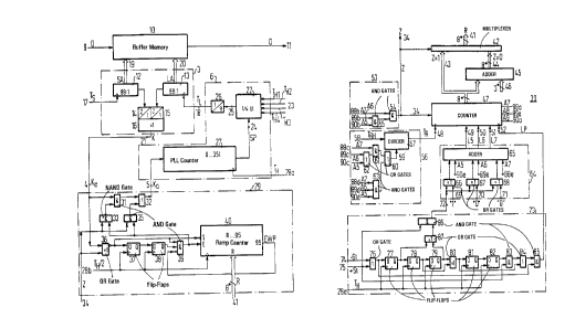
Figures 7 and 8 together show the timing recovery
device according to the invention. At the top, Figure 7
contains the timing recovery device already shown in
Figure 3, and at the bottom a ramp generator 29 as part
2~'~6~3~
- g -
of the phase-jump compensator 7. Figure 8 shows with a
ramp generator control device 30 a part of the phase-jump
compensator 7 still missing in Figure 7. Figure 9 shows
a diagram to explain the process sequence.
The ramp generator 29 in Figure 7 contains AND
gates 31, 35 and 3 9 , an OR gate 32 , a NAND gate 3 3 , an
exclusive OR gate 3fi, D-type flip-flops 37 and 38, and a
ramp counter 40. The retardation of the edges previously
described takes place in the ramp generator 29. The
designation "ramp generator" is based on the ramp-shaped
rising phase change generated by it. The numbers named
below can largely be changed.
The pulse-pause sequence of the correcting
quantity Re at input 4 is led to the output 5 via the AND
gate 31 and the OR gate 32, to the extent that the latter
are conductive. The ramp counter 40 is advanced by an
auxiliary clock pulse of half frequency TH/2 at the
auxiliary clock pulse input 28b. If its counter reading
reaches the final value of EW=95, it is locked in this
state by means of a final value pulse EWP via the AND
gate 39 and the preparatory input E until the counter
reading is set to its starting value by a pulse at the
set input S. It is subsequently incremented once again,
and the sequence outlined is repeated. The ramp generator
29 obtains the starting value from the ramp generator
control device 30 in Figure 8 via a bus 41 having eight
lines 8*.
After a relatively long time without stuffing,
the ramp generator control device 30 transmits a starting
value R=95. In this state, the starting value R and end
value EW of the ramp counter 40 are identical. It there-
fore remains at the counter reading R=95 even when it is
set to the starting value via the bus 41. During the
counter reading end value of EW=95, the preparatory input
E is at zero. Consequently, the NAND gate 33 and the AND
gate 35 are blocked and, for their part, drive the AND
gate 31 and the OR gate 32 in such a way that the cor-
recting quantity Re is not changed towards the output 5,
2~76~39
- to -
as is shown in Figure 4, sequences al and bl.
If, now, positive stuffing +St occurs, the ramp
generator control device 30 decreases the starting value
to R=95-32=63 and sets the state of the counting direc-
tion signal Z at the counting direction control terminal
34 to logic "1" . The ramp counter 40 remains locked at
first, however, since the preparatory input E has a state
of logic "0". The effect of the state of logic "1" of the
counting direction signal Z is that the pulse-pause
sequence of the correcting quantity Re is present
unchanged at the output of the exclusive NOR gate 36.
The state of the ramp counter 40 firstly remains
unchanged during a state of logic "1" of a pulse-pause
sequence of a correcting quantity R8. The ramp counter 40
is set to a starting value of R=63 during the following
pause with the logic state "0". The preparatory input E
remains, however, at logic "0", since the output of the
exclusive NOR gate 36 also has the logic state of "0" .
The output of AND gate 39 goes to logic "1" with the
start of the following pulse of the correcting quantity
Re, resulting in the release of the ramp counter 40. The
switching on of the two D-type flip-flops 37 and 38 is
technically determined and prevents metastable states.
The state of logic "1" at the output of the AND gate 39
blocks the AND gate 31 via the NAND gate 33, resulting in
a state of logic "0" for the correcting quantity Ra. The
ramp counter 40 increases its counter reading by one with
each period of the auxiliary clock pulse T$. It reaches
the value 95 after thirty-two periods. If the final value
pulse EWP changes to a state of logic "1", the output of
the AND gate 39 goes to a state of logic "0", and the
ramp counter 40 remains stationary at the state 95. At
the same time, the AND gate 31 is released via the NAND
gate 33, resulting in a state of logic "1" for the
correcting quantity Re. The frequency of the auxiliary
clock pulse TH and changes in the starting value R after
stuffing must be tuned such that the integration time of
the ramp counter 40 corresponds precisely to the temporal
~0'~6~~9
- 11 -
delay in the falling edge of the pulse-pause sequence cl
in Figure 4. During the following pause of the correcting
quantity Ke, the ramp counter 40 is set once again to the
starting value R and the sequence is repeated. The ramp
generator control device 30 now increases the starting
value R at regular intervals in each case by one until
the value of R=95 is reached once again, unless the
starting value R has previously been changed appropriate-
ly by a new stuffing process. This sequence is shown by
the sequences cl and dl in Figure 4.
The process proceeds correspondingly after
negative stuffing -St. The ramp generator control device
30 sets the state of the counting direction signal Z at
the counting direction control terminal 34 to logic "0".
The correcting quantity Re is present inverted at the
output of the exclusive NOR gate 36. By contrast with
positive stuffing +St, the AND gate 31 remains perma-
nently open. Controlled via the AND gate 35 and OR gate
32, the pulse duration is lengthened by the falling edge
of the correcting quantity Re. See the sequences el and fl
in Figure 4.
Figure 9 shows initial values A and starting
values R for a relatively long sequence without stopping
up to the instant tl, for positive stuffing +St up to the
' 25 instant tl, for negative stuffing -St up to the instants
t2 and t3, and for a compensated response between the
instants t4 and t5. One compensation process was inter-
rupted prematurely in each case at the instants tl, t2
and t3.
Figure 8 shows the ramp generator control device
30. The latter contains a multiplexes 42 operating as a
data selector, a full adder 45, an 8-bit initial value
counter 47, a counting direction control circuit 53, a
ramp clock pulse control circuit 56, an adder 64 and an
adder control 73.
The counting direction control circuit 53 con-
tains AND gates 54 and 55. The ramp clock pulse control
circuit 56 has a 3:1/1:1 divider 57, OR gates 60 and 62
20'~6~39
- 12 -
. as well as AND gates 61 and 63. The adder 64 comprises
a
full adder 65 and exclusive OR gates 66, 67 and 68.
Finally, the adder control 73 contains OR gates 76 and
84, D-type flip-flops 77, 78, 79, 81 and 82, exclusive
OR
gates 80 and 87 as well as AND gates 83, 85 and 86.
The core of the ramp generator control device 30
is formed by the initial value counter 47. The latter is
a commercially available counter whose upwards or down-
wards counting direction depends on the logic state "1"
or "0" of the counting direction control terminal 34.
Counting is upwards in the chosen example for the state
of logic "1". The clock pulse driving the initial value
counter 47 is the ramp clock pulse TR which is present
at
the ramp clock pulse input 48 and whose frequency deter-
mines the counting rate . Present as a binary number at
the output-side bus 43 of the initial value counter 47
is
a counter reading A thereof.
The binary number "01100000", whose digit posi-
tions are designated by A7 to A0, corresponds to the
average decimal initial value of A = 96. Thus, A7=0, A6=1
and A5=1.
If these values for A5, A6 and A7 are applied to
the AND gates 54 and 55, a logic state of "0" occurs at
the output 34 of the AND gate 54, which effects a down-
wards counting of the initial value counter 47. For
decimal values A<96, A7=0, and A6 and A5 are not both
one. Given this combination, a state of logic "1" occurs
at the output 34 of the AND gate 54, which triggers
upwards counting of the initial value counter 47. The
consequence of this is that the counter reading of the
initial value counter 47 changes periodically with the
ramp clock pulse TR between the decimal values A=96 and
A=95 as long as no charging pulse LP occurs at the
charging pulse input 52.
After the occurrence of charging pulse LP, the
counter reading of the initial value counter 47 changes
to the code word L5, L6 and L7 present at the charging
inputs 49 to 51. Thus, A7 assumes the value L7, A6 that
20'~~~3~
- 13 -
of L6, and A5 that of L5. The values of A4 to AO are not
changed.
The generation of the charging pulse LP and the
correct setting of the state of the control input 72 of
the adder circuit 64 takes place in the adder control 73.
If in the latter either a logic "1" for a negative stuff-
ing -St is applied to the input 74, or the logic "1" for
positive stuffing +St is applied to the input 75, the
output of the OR gate 76 likewise assumes the state of
logic "1". This state is transmitted with the aid of the
auxiliary clock pulse TH at the auxiliary clock pulse
input 28a in a stepwise fashion via the D-type flip-flops
77, 78 and 79. If the logic "1" is present at the Q
output of the D-type flip-flop 77 and a logic "0" at the
Q-output of the D-type flip-flop 79, or vice versa, the
exclusive OR gate 87 transmits a logic "1" to the AND
gate 86. If, furthermore, a logic "1" is present at the
input 75, a logic "1" likewise occurs at the control
input 72.
When different logic states are present at the Q
output of the D-type flip-flop 78 and at the Q output of
the D-type flip-flop 79, the exclusive OR gate 80 trans-
mits a logic "1". The latter is transmitted with the aid
of the auxiliary clock pulse T$ in a stepwise fashion via
the D-type flip-flops 81 and 82 to the first input of the
AND gate 83. If a logic state of "1" is simultaneously
present at the input 75, a logic "1" likewise occurs at
the output of the AND gate 83. If this is the case, or if
the output of the exclusive OR gate 80 is in the state of
logic "1", the OR gate 84 passes this state on to the
first input of the AND gate 85. If, now, the output of
the OR gate 76 is simultaneously in the state of logic
"1", the AND gate 85 transmits a charging pulse LP to the
charging pulse input 52 of the initial value counter 47.
In the adder 64, the adder input 69 is set to the
state of logic "1", the adder input 70 to the state of
logic "0", and the adder input 71 to the state of logic
"0~~,
2Q'~~~~~
- 14 -
In the case of negative byte stuffing - which
corresponds to an acceleration of the incoming data D by
eight UI - the decimal initial value A must be increased
by thirty-two.
If, in the case of negative byte stuffing -St,
the control input 72 receives a logic "0" at the control
input 72, a logic "1" occurs at the output of the exclu-
sive OR gate 66, a logic "0" appears at the output of the
exclusive OR gate 67, and a logic "0" appears at the
output of the exclusive OR gate 68. The code word formed
by the three exclusive OR gates 66 to 68 then runs,
beginning with the most significant digit position,
"001" . If the code word "011" is used for this purpose
for example for A7, A6 and A5, a code word "100" for the
decimal number 128 is produced at the charging inputs 51,
50 and 49 of the initial value counter 47 for L7, L6 and
L5. The counter reading is increased by decimal thirty-
two with the charging pulse LP now following.
In the case of positive byte stuf f ing +St, the
counter reading of the initial value counter 47 must be
reduced by a decimal value of thirty-two. If a logic "1"
appears for positive byte stuffing +St at the control
input 72, the output of the exclusive OR gate 66 receives
a logic "0", the output of the exclusive OR gate 67
receives a logic "1", and the output of the exclusive OR
gate 68 receives a logic "1". Thus, starting with the
most significant digit position a code word "110" is
present at the exclusive OR gates 66, 67 and 68. Added to
the code word "011" for A7, A6 and A5 selected above as
an example, the sum of L7, L6 and L5 produces a code word
"001" without carry. This code word, which contains the
decimal number thirty-two is accepted with a charging
pulse LP at the charging pulse input 52 as the initial
value A=32 of the initial value counter 47. In the next
period of the auxiliary clock pulse Tg at the auxiliary
clock pulse input 28a, the control input 72 receives the
logic state of "0". The exclusive OR gate 66 now assumes
the logic state of "1", the exclusive OR gate 67 the
2~'~~~39
- 15 -
logic state of "0", and the exclusive OR gate 68 the
logic state of "0". The full adder 65 now adds the code
words "001" and "001". The result of L7, L6 and L5 is a
code word "010". This corresponds to the decimal value
64
and is accepted with the next charging pulse LP at the
charging pulse input 52 as the final initial value A by
the initial value counter 47.
If a logic "1" is present at the switching input
59, the ramp auxiliary clock pulse T~ is passed and
divided in the ramp clock pulse control circuit 56 by the
3:1/1:1 divider 57 as ramp clock pulse TR to the output
41. If the switching input 59, by contrast, has the logic
state of "0", the ramp auxiliary clock pulse T~ is
divided 3:1 before it passes to the output 48 as the ramp
clock pulse TR. The output of the AND gate 61 now receives
a state of "1", if the code word A7, A6 and A5 is either
"101", "110" of "111". The output of the AND gate 63
assumes the state of logic "1" when the code word A7, A6
and AS is "000". The OR gate 60 then supplies the switch-
ing input 59 with a logic "1" if a logic "1" is present
either at the output of the AND gate 61 or at the output
of the AND gate 63. A logic "0" can occur at the switch-
ing input 59 only if A7, A6 and A5 form the code words
"001" "010" or "011". The decimal values then lie between
thirty-two and one hundred and fifty-nine.
The initial value A transmitted by the initial
value counter 47 must now be converted to the starting
value R of the ramp counter 29. If A < 96, the pre-
liminary starting value is simply passed on as the final
starting value R via the bus 43, the multiplexer 42 and
the bus 41. If A > 95, the preliminary starting value is
converted in the adder 45 according to the formula
R=191-A, by feeding it via the bus 46 the binary number
"010", which corresponds to the decimal number 64 in the
digital positions A7, A6 and A5, and the result is
inverted. The latter is forwarded via the multiplexer 42
and the bus 41.
_ 16 _ 2~'~6~~9
If no stuffing processes have occurred for a
relatively long time, as already described A changes
between the decimal numbers 95 and 96. In both cases,
however, R=95; the ramp counter 40 is thus constantly fed
R=95.