Note: Descriptions are shown in the official language in which they were submitted.
CA 02076094 2001-11-19
PROCESS AND DEVICE FOR THE PRODUCTION OF A REFLECTION-REDUCING
COATING ON LENSES
The invention relates to a process and a device
according to the preamble of Patent Claims 1 and 10.
With lenses the problem very often arises of applying a
protective coating which is light-permeable and yet reflection-
reducing. This applies for camera lenses as well as also for
lenses of eye glasses. In the case of inept or careless handling
by the user, eyeglasses can be subjected to extreme stress which
cases scratching not only of synthetic glasses but also of
silicate glasses. For surface damages as a rule sharp objects
are responsible which are drawn across the surface under
pressure. That can be, for example, sand with its sharp edges in
a polishing cloth or the case of the glasses but also rough
tissue.
Because they combine the property of low weight and
greater resistance to breakage with the possibility of individual
coloring, synthetic glasses are used increasingly more often.
However, they have the serious disadvantage that their surfaces
which are considerably softer compared to silicate glasses are
very susceptible to mechanical damage.
As a synthetic material for lenses duroplastics are used
widely which comprise macromolecules chemically closely enmeshed
with one another. They are most often very brittle at room
temperatures. In addition, they are temperature stable, not
weldable, insoluble, and only weakly swellable. One duroplastic
preferred in lens systems used for eyeglasses is CR 39 which is a
diallyldiethylene glycolcarbonate. Only very recently, apart
from these synthetic materials used nearly exclusively in lens
systems for glasses, other synthetic materials such as
polymethylmethacrylate (PMMA), polystyrene (PS), and
polycarbonate (PC) have been employed.
If, for example, a CR 29 synthetic is to be provided
with an appropriate protective covering, the problems of
detachment of the protective layer from the lens body, the
difference in heat expansion of protective layer and lens body as
well as in many cases the low temperature stability of the
protective coating must be solved.
With silicate coatings the substrate is heated to a high
temperature of approximately 300°C whereby sufficient energy is
available for the coating molecules applied in a
CA 02076094 2001-11-19
- 2 -
vapor deposition process in order to generate defect-free dense
layers. In contrast, when producing a synthetic layer, the vapor
deposition as a rule must be carried out at low temperature.
In order to make available the energy required in this
case, the grown layers are bombarded with ions of an inert gas.
Additional ionization of the vapor particles and the reactive gas
reinforces the densification process in the layer condensation.
Apart from these so-called ion-assisted deposition
processes (IAD), the so-called plasma polymerization is also
known in which during the layer formation the properties of the
layer can be changed continuously so that, on the one hand, they
are adapted to the synthetic surface from the aspect of the
chemical structure and, on the other, form on the boundary to the
air a glass-like structure which has a very high mechanical
resistance.
A process for the production of transparent protective
coatings comprising silicon compounds is already known which is
used in the coating of synthetic substrates (DE-A-3 624 467 = EP-
A-0 254 205). In this process a chemical vapor deposition takes
place under the effect of a plasma (= plasma chemical vapor
deposition) onto a polymerizable monomeric organic compound from
the group of the siloxans and silazans wherein to the
polymerization process oxygen is supplied in excess. The plasma
is therein generated by means of high frequency between two
electrodes of which the one has the function of a cathode and is
connected with the substrates. Before the coating proper the
substrates are exposed in an atmosphere comprising a noble gas to
an ion bombardment by glow discharge in the presence of the
organic compounds.
In another known process of plasma-enhanced coating of a
substrate with a polymerizable silicon-comprising monomer the
monomers are restricted to silans, silazans or disilazans and the
plasma coating is carried out until a particular Taber wear index
is attained (EP-A-O 52 870).
A device is also known (DE-C-3 931 713) with which
optical lenses can be coated on both sides in a plasma-enhanced
process. This device comprises two electrodes between which are
disposed holding elements for the work
pieces to be coated. The holding elements therein are at a
defined electrical potential.
A similar process is known (EP-A-O 403 985) for the
pretreatment of transparent synthetic substrates intended for
vacuum coating. It has been found that through plasma
CA 02076094 2001-11-19
- 3 -
bombardment of the substrate surface this surface is changed in
such a way that the subsequence layer can be applied with a high
degree of adhesive strength.
In a further device for the coating of substrates a
vacuum chamber is provided with a substrate carrier disposed in
it and having a plasma generator, a magnet and an electron
emitter wherein, in addition, in the vacuum chamber a device for
the generation of atoms, molecules or clusters of the materials
for the generation of the layer on the substrates is disposed,
which is located immediately next to the plasma generator and
opposite the substrates (EP-90123712.3, K.Matl, W. Klug, A.
Zoller: Ion assisted deposition with a new plasma source, Paper
presented at the Sec. PSE Conf., Garmisch-Partenkirchen 1990).
One advantage of this device reside therein that, in contrast to
earlier devices of the ion-assisted deposition (IAD), it can act
upon substrate holders having a diameter of approximately 1m with
high plasma density.
Moreover, antireflection coatings are know which are
applied onto synthetic lenses and comprise for example two layers
of which the first layer is a Si02 layer and the second layer a
Si0 layer (De-OS 27 39 044, Figure 1A).
Further, antireflection coatings are known comprising
four or more descrete layers wherein for example, beginning at
the substrate, the layer sequence is as follows: SiO, SiOz, CeOz,
SiOz, CeOZ (DE-OS 38 18 341).
DE-A-39 09 654 describes a reflection-reducing system on
substrates of plastic resin comprising a first layer of Si0 and a
second layer of SiOz. Herein the second layer merely serves for
improving the breaking strength and, therefore, has a thickness
of only 10 nm to 60 nm.
A mar resistant coating formed on a substrate of
plastics is also known wherein the coating has a thickness of 1
~m to 10 um (US-A-3 811 753). However, the combination of mar-
resistance and adhesive strength cannot be achieved with this
coating.
CA 02076094 2001-11-19
- 3a -
Further, it is known to apply a coating of 4 ~.m on
lenses made of polymer which consists of vaporized glass, more
specifically borosilicate glass (DE-A-25 38 982). Glass is made
of Si02 to only 80 per cent. Further, the thickness of the base
coating of Si0 and Si02 on which the glass is vaporized is not
indicated.
With a further known reflection-reducing system
consisting of two or three separate coatings first a homogenous
layer of Si0 or an inhomogeneous coating of Si0 and a substance
of a higher refractive index are applied to an object (DE-A-22 10
505). However, the degree of oxidation of the first Si0 layer is
not indicated. Further, only the refractive index is
inhomogeneous, but not the hardness of the layer.
It is also known to utilize Si0 having an optical
thickness of h/4 and 1~/2 for reflection reducing of polycarbonate
and other synthetic substrate materials (US-A-3 356 522; US-1-4
497 539). No distinction is made between coatings having good
adhesive strength and abrasion-resistance properties.
With another known antireflection coating system for
lenses of a synthetic polymer a first coating is made of a
compound of Si0 and SiOZ having an index of refraction of 1,8 and
an optical thickness of 1~/4 (=approximately 70 nm) and further
coatings of Ti02, Ce02, A1z03 and Si02 having a refractive index
of 1~/4 or 1~/2, respectively (DE-C-27 38 044).
Lastly, a process for the production of synthetic
objects with hard coatings is also known, in which a layer based
on silicon is disposed on a foundation material and onto this
layer a Si02 film is applied (EP-A-O 266 225). The SiOz layer is
herein applied by means of a vacuum vapor deposition process
preferably in an ion-plating process.
The invention is based on the task of creating a
scratch-resistant coating of eyeglasses, lenses and the like
comprising a relatively soft synthetic material.
In one aspect the present invention provides an
optical lens comprising a transparent plastic material substrate
and a first layer of Si0 which is disposed directly on the
substrate and which has a thickness of one atomic layer to 50 nm,
and a second layer of SiOz on the first
CA 02076094 2001-11-19
- 3b -
layer. The second layer has a thickness of at least 500 nm and
comprises at least two regions having different hardness, the
region having the lower hardness being adjacent to the first
layer.
In another aspect, the present invention provides a
method for the production of a layer with nonhomogeneous
hardnesses on a transparent plastic material substrate in a
plasma coating installation. The method comprises the steps of:
First arranging one or more transparent plastic-
material substrates in a substrate holder.
Si0 is then evaporated in an evaporator with
simultaneous irradiation of the substrate with a
plasma from a plasma source to form a layer of Si0
having a thickness of one atomic layer to 50 nm.
SiOz is then evaporated in an evaporator with
simultaneous irradiation of the substrate with a
plasma from a plasma source in which process either
the plasma power and/or the gas pressure and/or the
coating rate is altered so that a layer of Si02 having
a thickness of at least 500 nm and having
nonhomogeneous hardness is formed on the Si0 layer.
In yet another aspect, the present invention provides
for an apparatus for performing the above method. The apparatus
includes a chamber in which plasma can be generated, a substrate
holder for holding one or more transparent plastic-material
substrates, a plasma source opposite the substrate holder, an
evaporator next to the plasma source containing SiO, an
evaporator next to the plasma source containing Si02 granules, at
least one ring magnet above the substrate holder, means for
controlling the plasma power of the plasma sources, means for
controlling the gas pressure, and means for controlling the
coating rate of the evaporator containing Si02 granules.
The advantage achieved with the invention resides in
particular therein that the tensions between the relatively soft
synthetic substrate and the hard coating are decreased.
CA 02076094 2001-11-19
- 4 -
The Si0 layer is selected to be of minimum thickness
because SiO, for the application according to the invention, has
optically undesirable properties and is therefore used primarily
for the purpose of ensuring adhesion. With increasing layer
thickness of Si0 the reflection increases. This leads to an
increase of the oscillations of the reflections curve (r = f(~))
brought about by the succeeding thick SiOz layer. Moreover, Si0
is not absorption-free. A thin Si0 layer therefore keeps the
undesirable reflections and absorption within reasonable limits
and yet fulfils the requirements made of the adhesive strength.
The SiO2protective layer, in contrast, must be relatively thick,
i.e. > 500 nm since otherwise the requirements made of the
scratch-resistant are not met. Thinner SiOz layers at the given
stress break down even if they are very hard. Moreover, they
cause undesirable oscillations of the reflection curve. In the
case of thicker Si02 layers the oscillations are also present,
however, the wavelength interval of the minima and maxima becomes
smaller with increasing layer thickness so that on visual
inspection no disturbing interference effects can be observed.
Embodiment examples of the invention are depicted in the
drawing and will be described in greater detail in the following.
Therein show:
Fig. 1 a two-layer configuration on a synthetic lens substrate;
Fig. 2 a three-layer configuration on a synthetic lens
substrate;
Fig. 3 a seven-layer configuration on a synthetic lens
substrate;
Fig. 4 a schematic representation of a plasma IAD process for
the generation of thin layers.
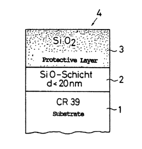
In Figure 1 is depicted a lens substrate 1 of a
synthetic material, for thickness CR 39, which is provided with a
very thin Si0 layer 2 having a thickness of one atom up to 20 nm.
This layer 2 serves essentially for the purpose of effecting a
better adhesion of a protective coating 3 with a
5
thickness of at least 500 rnn of Si02.
As has been found a Si02 layer applied directly adheres only poorly on
synthetic materials. In so-called boiling tests coated substrates are
cyclically imm~errrsed for a defined time in a boiling salt solution
c~nprising
for example 5% NaCl in water. They are subsequently plunged into cold water.
A layer of Si02 applied directly on a synthetic material be~mes very rapidly
detached in such boiling tests, for example after 5 to 10 minutes. In
fast, if a Si0 layer 2 is disposed between the Si02 layer 3 and the
substrate of synthetic material which is coated under simultaneous plasma and
ion bcanban~ent with a resistance vaporizer boat or an electron beam gun, the
( adhesion of the Si02 layer 3 increases considerably. Even after a boiling
test lasting 40 minutes no impairments on layers 2 arid 3 could be detected.
With the thick Si02 layer 3 the wear properties are significantly
improved relative to the synthetic substrate 1. CR 39, for example, has a
harr~ness of approximately 180 to 200 N/mm2. Dense quartz, in contrast, has a
hardness of 4500 N/nmn2. The hardness of the protective layer 3 can be
adjusted in a very broad range via the plasma and coating parameters.
Thresh special plasma coatings harc~zess values of approximately 1000 N/imn2
up to nearly 4500 N/mm2 have so far been achieved.
The wear resistance increases basically with the hardness and the layer
thicla~ess wherein at a layer thick~ss beginning at appr~ci~mately 3 to 8 ~mn
a saturation effect in the wear resistance ocxurs as a fl~nction of the
haxtlness. In the production of very haul and consequently brittle layers,
strong tensions between layer and substrate are generated. For example CR 39
has a coefficient of thermal expansion of approximately 1 * 10'4/K while, in
contrast, the coefficient of thermal expansion of quartz is almost
negligible. Accordingly, a 70 mm CR 39 lens expands by approximately 0.4 mm
at a temperature differexice of 80oC. The expansion of quartz, in contrast,
is nearly 0. The tensions caused thereby make great dmnaryds made on tha
adhesion of the layer. It is therefore useful to break down at least a part
of the tensions in the layer itself. This is achieved via a hardness
gradient i.e. the hardness increases frcen the interior on the substrata in
the ~ztwar~d direction. For the production of the Si02 layer it is suggested
to use as the starting material Si02 instead of a suboxide. Si02 can be
vaporized with very laa vaporizer power. The temperature stress placed on
6
the sub:~trates can thereby be kept to a minimum during the production of the
thick protective layer.
By insetting a layer 5 between the Si0 and the Si02 layer the
oscillations in the reflection curve can be decreased considerably. This
layer 5 has preferably an index of refraction smaller than the index of
refraction of the substrate 1 and greater than the index of refraction of the
protective layer 3. If CR 39 is used as the substraate and if the protective
layer 3 oamprises Si02, the index of refraction of layer 5 is between 1.45
and 1.52. The thic3aless of layer 5 herein is approximately 80 to 120 rnn
which at a wavelength of light of 550 rmi corresponds to a quarter wavelength.
~ this measure the oscillations due to the thiclmess of the layer 3 are
atte~nxated.
Figure 3 depicts a variant in which as intermediate layer 6 a SiOx layer
is used wherein x is a value between 1 and 2. On the Si02 layer 3 is
disposed a carnbination of four father layers 7 to 10 which serve exclusively
for the purpose of reducing the reflection. These layers ocanprise
alternately Ta205 and Si02 wherein the uppermost layer is Si02.
The production of the layers takes place in the manner described in~the
following and in conjunction with Figure 4.
In a standard vac:uuin installation 20 the layers are deposited by means
of an electtron beam vaporizer 21 (see above Matl, Klug, Zoller). A plasma
source 22 is herein disposed in the center and on the bottarn 23 of the
installation 20 and directed onto an electrically insulating substrate holder
24. In the plasma soure-.e 22 is disposed a cylindrical electron-emitting LaB6
cathode 25 encompassed by a cylindrical anode 26 having a diameter of
approximately 50 mm. A glow discharge pla~na is generated wherein a noble
gas, primarily anon, is introduced via a line 28.
A cylindrical magnet coil 29 encloses the anode 26 and brings about
that the possibility for movement of the electrons generated by the plasma
is considerably increased in the axial direction and considerably decreased
in the radial direction. The electrons mwe in spiral form about the
magnetic field lines whereby the plasma reaches the coating chamber 20. On
the top 30 of the coating cumber 20 and above the substrate holder 24 is
provided an annular magnet coil 31 with an inner diameter greater than the
diameter of the substrate holder. The magnetic field of this ring magnet 31
7
and the magnetic field of the cylinder coil 29 are superim~sed and form a
guidance field for the electrons on their way frcan the cathode 25 heated
indirectly by a heater 27 and fed, in turn, by the energy supply 32, as well
as for the entire plasma between the plasma srntcce 22 and the substrate
holder 24. In front of the dame-form substrate holder 24 is generated a
dcane-form plasma boundary layer. Because the potential of the substrate
holder 24 relative to the plasma is negative, the ions are accelerated out of
the plasma botux3ary layer and bcm~ard a growing film which is thereby
densified. A significant advantage of the production process in Car~parison
to the conventional lAD processes with one ion source resides therein that
tY~~e ions starting out of a plasma boundary layer forming parallel to the
entire inner face of the substrate holder are acce7.erated over a short
distance. In the case of an ion source where the acceleration takes place
frcnn the bottoan of the chamber the conditions are different. In the device
according to Figure 4 the ions frown the plasma botmdaiy layer are not
influenced by collisions and energy losses. Moreover, the plasma extends
over the entire area between the plasma source 22 and the substrate holder
24 so that the ion sour.~ce basically covers the same area as the substrate
holder 24. With a conventional. ion sourve with grid extraction an extraction
grid area is required corresporbding nearly to the beamed upon area on the
substrate.
A reactive gas, for example 02, N2 is introduced into the Chamber 20 via
a line 34. Due to the plasma in the chamber 20 it is ionized and activated.
The vaporized material 35 of the electron beam gun 21 must also pass through
the plasma frcnn the substrate holder 24 so that it bec~es ionized and
activated.
the plasma source 22 is electrically insulated from the chamber 20.
Apart frcmn the supplied discharge voltage one therefore in addition also
obtains a potential difference between the s~ 22 and the chamber 20.
Tha source 22 assumes a variable positive potential relative to the Chamber
20 while the substrate holder 24 is nearly at the same potential as the
chamber 20. The ion energy is determined by the potential difference
between the anode tube 26 fed frarn a do current source 36 with a positive
potential, and the substrate holder 24. The variable potential of source 22
is a function of the discharge voltage, the partial pressures of the gases
8
and the strength of the magnetic field. Thresh the positive floating
potential of the electric field an electxic field is generated which reflects
the electrons between source 22 and substrate holder 24. If they do not
impinge on the anode tube 26 they are reflected on the cathode potential and
can again crane out of the sue. Consequently, osc311ati.ng electron paths
with an effective ionization and excitation of gas atcams and molecules are
obtained. Due to the repulsion effect generated by the electric fields in
the vicinity of the anode the plasma in front of the substrate holder 24 is
dcanirsated by ions. This can be recognized by the potential of the substrate
holder 24 which is approximately between 3 and 5 volts relative to the
( chamber wall 20. The discham~e parameters are up to 80 volts discharge
voltage, 70 A discharge current, and 5 kW plasma power. The pressures are
1 x 10'4 to 8 x 10'4 mbars with a ratio of 02: Ar of up to 4 : 1. The
described operation of the plasma source makes it possible to separate the
plasma generation process frarn the vaporization process.
All vaporizable starting materials, for example oxides and fluorides,
can be vaporized in the vaporizer 21 since no coupling between plasma source
and vaporizer source exists.
For the vapor deposition of a scratch-resistant Si02 layer, Si02
' granulate is used which is vaporized with electron beam generator 40 in the
electron beam vaporizer 21. For this granulate a relatively low vaporizer
power is required. In order to keep low the vaporizer power even in the
case of highly refractive material for example Ta205 a multic~tp crucible
with cups of ~ size is preferably used of which only one cx~p 41 is
depicted. After pumping the chamber 20 down to a pressure of < 2 x 10'5
mbars the vapor deposition of the layer system is carried out.
The Sio adhesion layer is deposited at a rate of appznximately 0.1 rmys.
The pla~na source 22 is added simultaneously with the opexiing of a vaporizer
diaphragm not shown. The source 22 is herein operated with pure azgon at a
partial pressure of approximately 2.5 x 10'4 mbars. The discharge curreant is
approximately 30 A at a discharge voltage of approximately 30 V. After
obtaining the desired layer thickness the plasma source 22 is switched off
simultaneously with the closing of the vaporizer diaphragm.
Subsequently, the vapor deposition of the thick Si02 protective layer
takes place. Herein the plasma source 22 is also operated with argon.
~~ r ~~~~~~'~
The hardness of the Si02 layer is a ftmction of the plasma dischazge
power i.e. current and voltage, the gas pressure, and the coating rate. The
hardness gradient of the layer is adjusted with these parameters.
Especially low hardness values are achieved with low plasma power (< 1 kW) at
relatively high pressure (approximately 6 x 10⁻⁴ mbars), and a high coating
rate (appzroximately 5 x 10 nm/s). The greatest harr3ness values were achieved
in experiments carried out with a plasma power of approximately 5 kW, at a
pressure of 1.5 x 10'4 mbars and at a rate of 0.1 nttS/s. After the desired
layer thic)mess has been arhi.eved, the plasma source 22 is switched off with
the closing of the vaporizer diaphragm.
Subsequently, the vapor deposition of the first highly refractive layer
Ta2o5 takes place. In principle, other highly refractive materials can also
be used such as for example titanium oxide, zirconitan oxide, etc. In the
highly refractive layers the plasma source 22 is also operated with argon at
a pressure of approximately 2 x 10'4 mbars. In addition, oxygen is
introduced into the chamber 20 through line 34 with a partial pressure of
approximately 4 x 10'4 mbars. An oxygen inlet directly into the plasma
source, analogously to inlet 28, is also possible. During the vapor
deposition of the tantalwn pentoxide layer the plasma source is operated with
a discharge pacer of approximately 5 kW. The coating rate is approximately
0.2 n~/s. The next layer Si02 is deposited in principle like the Si02
protective layer and specifically at a pressure of 2 x 10'4 mbars, a plasma
power of apprrncimately 4 kW, and a coating rate of approximately 0.5 rm~/s.
The vapor deposition of the succeeding highly refractive layer takes
place with the same parameters as the first highly refracaive layer. The
last Si02 layer is deposited like the preceding Si02 layer.
The optimum production parameters of the ~ /4 SiC~ intermediate layer
for the attenuation of the oscillations of the spectral curve disposed
between the Sio layer arid the protective layer, are a ftinction of the
hardness and, consequently, the index of refraction of the protective layer.
The following parameters are suitable: pressure approximately 2 x 10'4
mbars, plasma power approximately 4 kW, rate approximately 0.1 rm~/s.
It is understood that for the generation of atoms, molecu7.es or clusters
of the materials, for example Sio or Si02, which are to be applied onto a
synthetic lens or the like, instead of an electron beam vaporizer also a
~~ ~ ..~ ~.
to
thermal vaporizer or a sp~xttexing cathode can be used. It is only esser~t3a1
that the plasma is generated in a device separated fran the electron beam
gun, etc. Thereby that the plasma is generated in the plasma source 22 and
the small particles to be applied in a vaporizer source 21, the uniformity of
the coatis is especially high. Moreover, the coating parameters caa~ be
adjusted largely ir~deper~dent-.ly of one ~, which is of great significaryoe
for the product3.on of layers with tcxbghness gradients.
The substrate holder 24 whose lowpx edge is denoted by 33, can be
rotated by means of a shaft 42. It can be provided on its underside with
rnm~exnus lenses or the like to be cbated. Moreover, the substrate holder 24
( can have a vaporizer protection not shoran which in the deposition of
ir~sul.ating materials prevents the coating of a portion of the surface of the
substrate holder with these insulating materials and consequently m~k~es
possible the drainiryg of electrical charges via the substrate carrier.
Further details of the device according to Figure 4 can be found in German
Patent A~lication P 40 20 158.9 and are therefore not described in i~rther
detail.
When with an arrangement according to Fig. 4 the plasma power is put down in
kW as a function of time this results in a straight line substantially
linearly
rising from 0,5 to 5,5 kW, whereas simultaneously the pressure falls almost
linearly from 6 s 10 4 mbar to 1 ~ 10 4 mbar. At the same time the rate
decre2ses from 5,5 nm/s to almost 0 nm/s.