Note: Descriptions are shown in the official language in which they were submitted.
1
"ENERGY MONITORING SYSTEM FOR A PLURALITY OF LOCAL
STATIONS WITH SNAPSHOT POLLING FROM A CENTRAL STATION°'
' This invention relates to load management for
electrically operated loads, and in particu7.ar to a PC
computer monitored system fox instantaneously ascertaining
the individual consumption of energy by users at several
locations behind the meter which has been installed by the
electrical utility company for computing the total energy
used from the main lines.
The electrical companies usually place at least
one meter at the junction of the main distribution power
lines with their customer consumption location, that it be
a factory, a house, a shop,' a business, or a residential
building, thereby to collectively monitor the kilowatts
drawn from the main AC lines on the basis of the sensed
voltage and current, and to compute the energy so as to
bill the customer according to actual demand. It is now
proposed to determine at the customer°s level how much at
a sublevel has been consumed, behind such an electrical
meter of the utility company, at each of the subloca~tions
of users in order that the billing can be divided and the
cost fairly distributed between them, that they be
residents, 'tenants, workshop craftsmen, or shopkeepers.
The specification of U.S. Patent No. 4,168,491
shows the control of the demand of energy consumed by
several users pertaining to a common building. The
purpose, there, is to stop the user's consumption whenever
it exceeds a predetermined limit. To this effect, when
power may be exceeded, from a central location all the
2
users in the group are distributively switched OFF, either
cyclically and for a certain duration, or told to switch
OFF.
It is known from the specification of U.S.
Patent No. 3,937,978 to control remotely electrical loads,
such as multi-unit lodging eastablishments, power sensing
being used to deenergize a load having excessive consump-
tion.
From the specification of U.S. Patent No.
3,906,242 it is known to monitor loads under programmed
peak load reduction from a computer load center operating
with a signal ~transmit~ter upon a plurality of installa-
tions having their local signal receiver and load limiter.
The specification of U.S. Patent No. 4,090,062
shows an energy demand controller for a house, or a
building, having separated heaters and appliances, each
having a local control unit and an intermediary switch.
In the specification of U.S. Patent No.
4,100,426 load controlling is accomplished with plug--in
modules which are part of a standard package associated
with the respective loads for a given installation.
The specification of U.S. Patent No. 4,206,443
discloses protective load disconnection is remotely
performed at a single control input terminal from a master
controller and monitoring unit.
The specification of U.S. Patent No. 4,874,926
discloses the use of low voltage thermal relays planed
adjacent to the downstream or outlet side of a residential
circuit breaker in the in-residence power distribution
lines leading to individual electrical heating elements.
The specification of U.S. Patent No. 4,164,719
is for a load management application wherein, between the
local load and the power input, a conventional circuit
breaker is combined with, a management module.
The specification of U.S. Patent No 4,178,572 is
provided with a contactor-circuit breaker arranged for
mounting in the same panelboard having the load circuit
breaker serving for energization.
' CA 02076211 1999-07-16
3
The specification of U.S. Patent No. 4,308,511
relates to a load management circuit breaker containing an
electronic package and a remote-controlled switch,
associated with an electric energy meter and a master
control transmitter connected through a line of communica-
tion.
The specification of U.S. Patent No. 4,806,855
relates to a system for rating electric power transmission
lines. The system there described. includes current
sensor-transmitter for multiplexed transmission by
telecommunication-link to a computer. ,'
The specification of U.S. Patent No. 4,219,860
shows digital overcurrent relay apparatus using sampling
with digital conversian in relation to the monitored AC
current.
In the specification of U.S. Patent No.
4,423,459 a solid state circuit is illustrated involving
AC current monitoring by sampling and digital conversion.
In the specification of U.S. Patent No.
4,682,264 a microprocessor-based solid-state trip unit
processes digital signals derived from current sensors.
According to one aspect of the invention there
is provided an electrical monitoring system for use on an
AC line, comprising a circuit breaker installed on said AC
line, said system comprising a backpack unit mounted on
said circuit brealker and having an opening through which
said AC line is passed, said backpack further having
mounted therein transducer means cooperating with said AC
line for deriving analog signals representative of AC line
current and voltage, analog to digital means for converting
said analog signals to digital signals, and processing
means for computing electrical measurements from said
digital signals; a remote monitoring device for retrieving
said computed electrica:L measurements; and bi-directional
digital communication means linking said backpack unit and
said remote monitoring device for establishing a data
highway therebetween.
CA 02076211 1999-07-16
4
Preferably, the transducer means comprises a
current transducer inductively coupled with the AC line and
a voltage metering device connected to the AC line.
The monitoring system of the invention may
further include a PC board mounted in the backpack unit
having an opening around which is mounted the current
transducer and wherein said AC line is passed through said
opening and through said current transducer.
Preferably the analog to digital means and the
processing means are integrated in a CMOS monolithic
circuit.
The monitoring system of the invention may
further include a second PC board mounted in the backpack
unit on which the CMOS monolithic circuit is mounted.
According t:o another aspect of the invention
there is provided an electrical monitoring system for use
behind a collective electrical meter having a plurality of
AC lines associated therewith, said system comprising a
plurality of circuit breakers wherein each one of said AC
lines has installed thereon one of said plurality of
circuit breakE~rs, a plurality of backpack units
individually mounted on each of said circuit breakers, each
of said backpack units having an opening through which said
AC line passes so that: a backpack unit mounts to a circuit
breaker and an AC line passes through the backpack unit and
connects to the circuit breaker, and in that each of said
backpack units further has transducer means cooperating
with said AC line for deriving analog signals
representative of AC line current and voltage, analog to
digital means for converting said analog signals to digital
signals, processing means for computing electrical
measurements from said digital signals, and storage means
for saving said electrical measurements; a remote
monitoring device for retrieving said electrical
measurements from each of said plurality of backpack units;
and bi-direction,~l digital communication means linking said
remote monitoring device to each of said plurality of
backpack unit: for establishing a data highway
therebetween.
CA 02076211 1999-07-16
Preferably the bi-directional communication
system is used at regular successive intervals by the
remote monitoring device to initially and simultaneously
address and command each of the plurality of backpack units
5 to store the electrical measurements whereby said remote
monitoring device may address and poll each of the
plurality of backpack units individually to retrieve the
stored electrical measurements.
Preferably, the transducer means comprises a
current transducer inductively coupled with the AC line and
a voltage metering device connected to the AC line. '
It i:~ further preferred that each of the
plurality of backpack units further has a PC board mounted
therein having an opening around which is mounted the
current transdu<:er and wherein the AC line passes through
said opening and through said current transducer.
The analog to digital means and the processing
means may be integrated in a CMOS monolithic circuit.
Preferably, each of the plurality of backpack
units further has a second board on which the CMOS
monolithic circuit is mounted.
30
CA 02076211 1999-07-16
6
10
The digital data-link used in the preferred
embodiment is of the type disclosed in the specification
of U.S. Patent Nos. 4,563,073; 4,644,547, and 4,866,714.
The invention is applicable to mere performing
of metering functions at the level of the several local
users with centralized monitoring and accounting of the
individual demand and energy billings. It is also
applicable to individual billing of the electrical utility
share under the company billing system which may include
peak-demand ratings, for instance.
The invention will now be described, by way of
example, with reference to the accompanying drawings in
which:
Figure 1 is a schematic diagram of a panelboard
installation incorporating the energy monitoring system
according to the invention coupled, through individual
backpack units, to a plurality circuit breakers serving
local users;
Figure: 2A and 2B are front and top views of one
of the circuit breakers of Figure l;
.,
Figures 3A, 3B and 3C are front, top and side
views of one of the backpack units of Figure 1, whereas
Figure 3D is like Figure 3B, but with a circuit breaker
shoran coupled to it;
Figures 4A and 4B are front and top views of one
of the circuit breakers of Figure 1, the two opposite
conductor terminals being shown in Figure 4A attached -to
the respective incoming and outgoing cable lines, the
associated backpack unit being shown plugged-in on the
outgoing local load line side;
Figure 5A is, like Figure 3A, a front view of
one of the backpack units of Figure 1, with Figures 5B
and 5C showing 'two cross-sections of the backpack unit of
Figure 5A;
Figure 6A is a front view of the lug of the
backpack unit of Figures 3A, 3B, 3C, 5A, 5B or 5C, as it
is mounted near the rim of the printed-circuit board
opening through which a cable line is to be axially
passed; Figure 6B is a cross-section taken from Figure 6A;
Figure 7 shows side-by-side the two printed-
circuit boards of Figure 1;
Figures 8A and 8B are illustrating the internal
organization of a backpack unit built around two printed-
circuit boards, the latter being initially mounted side-
by-side (Figure 8A) before being folded and brought on top
of the other (Figure 8B) once assembled;
Figure 9 is an exploded view of the bottom
casing of the backpack unit and its cover, the functional
unit of Figure 8B being shown nearly sandwiched
therebetween;
Figures 10A and 10B are separate views, taken in
perspective, of the bottom casing and the cover used for
the backpack unit of Figure 9;
Figure 11 shows diagrammatically the mechanical
and electrical connections within the backpack unit;
Figure 12 illustrates the energy monitoring
system according to the invention with a PC computer
operator control station, connected to a plurality of
~~"~~i~~ ~~
8
slave backpack units, each backpack unit being coupled, or
to be coupled, to a corresponding ci:rcui~t breaker serving
the local electricity user, monitoring being effected
through a common line of communication, with an optional
local data collecting station inserted therein;
Figure 13 illustrates in an exploded view the
face-to-face relationship bei~ween the two printed-circuit
boards which inside the backpack unit establish an
interface between the circuit breaker terminal sensing
functions and the lower-link functions of the PC computer
communication line:
Figure 14 is a diagram illustrating the current
and voltage sensing functions involved in the transducer
printed-circuit board:
Figure 14A shows the internal circuitry of the
printed-circuit board of Figure 14;
Figure 15 is a schematic representation of the
basic functions performed digitally by the printed-circuit
board interfacing with an INCOM communication line to the
PC computer;
Figure 1& is an overall view of the energy
monitoring system according to the present invention;.
Figure 16A shows the backpack unit according to
the presen°t invention mounted in an expanded mode slave
relationship with the INCOM communication line to the PC
computer;
Figure 17 is a diagram illustrating the INCOM
communication line connection with the digital printed
circuit board of a backpack unit through a Sure Plus Chip;
Figure 18A is a diagram showing the interface
between the INCOM communication line and the Sure Plus
Chip of Figure 17;
Figure 18B illustrates circuitry used in the
implementation of the diagram of Figure 18A;
Figures 19A-19C illustrate the overall cir-
cuitry of the digital printed-circuit of the backpack unit
according to the present invention;
~~~~~ ~..a
9
Figure 19D shows the connector associated in the
circuitry of Figures 19A-19C with the signals received
from the current and voltage printed-circuit board;
Figure 19E is illustrative of circuitry involved
for the power supply in the board of Figures 19A-19C;
Figure 24 illustratfa the angular distribution
about a circle of the 8 samples of the first octave under
the sampling process according to the preferred embodiment
of the invention;
Figure 21A illustrates on a half-cycle, the
distribution of two consecutive octaves of samples,
whereas Figure 21 B is the corresponding half-cycle of the
fundamental waveform; .
Figure 22A is a diagram showing the interface
between the inputted signals with the chip SP; Figures 22B
and 22C show the voltage and the current mode of chip
operation in the A/D conversion process, with Figures 22D
and 22E being their equivalent circuits, .respectively;
Figure 22F shows circuitry of the chip SP performing a
change from voltage to current mode depending upon the
input signals; and Figure 22G gives the reference to a
fundamental cycle for the two afore-stated modes;
Figure 23 is a diagram illustrating the cir
cuitry involved in tire chip SP of Figure 19 for the
current and voltage modes of Figures 22B and 22C;
Figures 24A, 24B and 24C are flowcharts
illustrating the operation of the energy monitoring system
when at the user's station sampling current and voltage,
calculating energy and accumulating an instantaneous total
of energy according to the present invention;
Figure 25 is a block diagram illustrating
snapshot operation from the PC computer station of the
energy monitoring system according to the invention;
F:Lgure 26 is a general block diagram of the
energy monitoring system;
Figures 27A, 278, and 27C are flowcharts
explaining the operation of the energy monitoring system
of Figures' 25 and 26;
~~~ ~~~1 ~.
Figures 28A, 28B, 28C, 28D and 28E axe flowcharts
illustrating the operation of the energy monitoring system
at the user's station sampling current and voltage,
calculating energy, RMS current and voltage, average power,
apparent power, reactive power, and the power factory and
Figure 2~ is a block diagram illustrating the
operation of the computer station acting in conjunction with
CA 02076211 1999-07-16
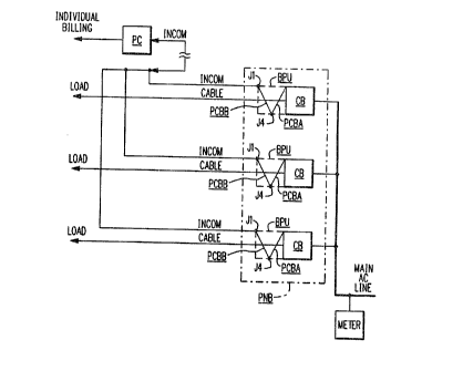
Figure 1 shows a diagrammatical view of the
energy monitoring system embodying, several backpack units
each coupled with one of several'circuit breakers CB
which are part of a panel board ~ through which the main
5 electrical AC :lines are interconnected with local cables
leading individually to serve separate user's loads. Each
backpack unit includes two printed-circuit boards PCBA and
PCBB which are interconnected at J4, one (PCBA) for
effecting current transducer and voltage sensing functions
10 with the circuit breaker, the other (PCBB) for deriving
digital information therefrom (at junction J1) which is
transmitted through a telecommunication channel INCOM for
bilateral transmission with a PC computer PC. As a result
of energy monitoring through a selective combination of
the several printed-circuit boards with the PC computer,
it is possible from the PC computer station to establish
instantaneously individual load billings for the different
local users, at a stage which is after the collective
Meter (Figure 1) installed by an electrical system
supplying energy through the main AC lines.
Figures 2A and 2B are front and top views,
respectively, of a circuit breaker which can be installed,
as illustrated by CB in Figure 1. The circuit breaker,
typically has three female terminals TA, TB and TC (for the
respective poles, in a three-pole example) upon which the
individual local cables (each shown as only one pole in
Figure 1) are attached between a screw (SCW) driven member
39 engaging the cable and a stopping member 38 held by a
bracket 38~ within the terminal (TA, TB, or TC). The
handle is protruding at 42, for manual control, namely, on
the front plane of the panel board PNB of Figure 1.
Figures 2A and 2B are taken from the specification of U.S.
Patent No. 3,892,298. As shown in Figure 1, the local
cable, before entering with its open end the terminal of
the circuit breaker, is passed through the two printed-
circuit boards 1~CBA and PCBB, which have been provided,
each with a proper opening (not shown). The other side of
CA 02076211 1999-07-16
11
the circuit breaker is likewise connected through terrain-
als to the AC 7.ines from the Electrical Company.
Figures 3A, 3B and 3C are front, top and side
views of one of the backpack units BPU of Figure 1, 'shown
_ as a housing comprising a bottom casing BX and a cover CV,
with protruding blades, or lugs, LG, one for each pole of
a three-pole circuit breaker such as the one of Figures 2A
and 2B. J1 is the connector, inserted within the PU
housing, into which the telecommunication line INCOM of
l0 Figure 1 is plugged-in. Three circular openings (OA, OB,
OC) are visible (on Figure 3A) which are provided
crosswise through the entire housing and the internal
printed-circuit board. assembly (PCBA and PCBB on Figure 1)
of the backpack unit B~ .A lug or stab LG is seen mounted
in each hole (OA, OB, OC). The local user's cable
associated with one pole of the circuit breaker is passed
through a corresponding opening (OA, OB, or OC) of the
circuit breaker housing, and beyond it, its open end is
placed along the lug LG, or conversely, within the terminal
(TA, TB, or TB in Figure 2A) of the circuit breaker, so
that cable conductor and lug become held together, while
being closely pressed under the tight grip of a screw for
good electrical contact. Figure 3D shows the backpack unity
BPU plugged-in with the circuit breaker ~B.
Figure: 4A is a side view of the circuit breaker
of Figure 3D (wh.ile Figure 4B is a top view thereof)
showing the naked end of the electrical cable from the
local user engaged with the terminal conductor 38 of the
breaker and pressed against it under a screw SCW. The
local user's cable passes across the housing of the
backpack unit BPU and through two parallel printed-circuit
boards PCBA and PCBB. Although in Figure 1, printed-
circuit PCBA is shown closer to the circuit breaker CB
whereas the other printed-circuit PCBB appears on the
opposite side a:nd closer to the communication line INCOM,
in Figure 4A the PCBB printed-circuit board is shown
mounted close to the circuit breaker, a lug LG being
attached to it and extending therefrom directly to the
.'A.
12
outside for insertion into the terminal (TA, TB or 'fC of
Figure 2A). Consequently, from a rivet of fixation 30,
mounted on printed-circuit lboard PCBB, is derived a
signal characteristic of the phase voltage which is passed
to the other printed-circuit :board (PCBA), via a resistor
R4 (for phase A, for instance). As will be explained in
detail hereinafter, printed-circuit board PCBA supports
transducers which sense the phase currents passing through
the local cable. Therefore, the sensed phase voltage
signal passed through R4 is also received by board PCBA.
Conversely, via an electrical connector J~, the current
and voltage sensed signals are together passed to the
PCBB printed-circuit. There, after digital conversion and
digital treatment, there will be information passed,
through connector J1 of printed-circuit board PCBB ,to the
INCOM line leading to a PC computer for central monitoring
of the energy consumed through the particular circuit
breaker and the local user's cable. ~fhe circuit breaker's
conductor 38 is mounted on a bracket 38°. The terminal
bare end of the cable is pressed with a screw against the
lug LG of the backpack unit, the latter being squeezed
between the cable and conductor 38. The AC line is fixed
inside the opposite terminal of the circuit breaker
directly against conductor ~O, the latter being mounted on
a bracket 40°, as generally known.
Figure 5A is a front view of a backpack unit,
like in Figure 3A, bearing cross-section lines F-F and A-A
to which are related the cross-sectional views of Figures
.5B and 5C, respectively. Figure 5C shows lug LG as
installed and mounted with its rivet 30. The parallel
printed-circuit boards have a circular opening (OA for
phase A, for instance) having a rim OP. The insulating
housing includes a bottom casing BX having a plastic boat
BT, extending across the openings of the two printed-
circuit boards (PCBA and PCBB), with an internal
cylindrical surface OP° of sufficient diameter to allow
the local cable therethrough. Boot BT, extends in
proximity of the rim OP of the printed-circuit boards. It
~Q'~ri<~.~:~.
13
starts from the bottom of casing BX until it engages at
the other end a complementary circular ridge EDG provided
on the bottom of the cover CV. The two ,are joined
together to close the space and provide insulation in the
gap between rim OP of the printed-circuit boards and the
axially mounted local cable.
Figures 6A and 6B show lug LG as it is mounted
on the printed-circuit board PCBB. Figure 5B is a cross-
section along line BB of Figure 6A. OP is the rim of the
opening oA (for phase A, instance).
Figure 7 illustrates how the two printed-circuit
boards are connected side-by-side. Each lug (one for each
of the respective openings OA, OB, OC in the case of a
three-pole circuit breaker) hG is mounted on board PCBB
with a rivet 3o which is electrically connected by line 10
to a resistor R4 (for opening oA and phase A), R5 (for
OB), or R6 (far OC) which are bridging the two edges of
the two printed-circuits boards. Printed-circuit PCBA
shows circular compartments ~T fox the current transducers
of opening OA, OB and OC, destined to surround the local
cable for sensing. The AC voltage representative signals
VA, VB, VC (derived through resistors R4, R5 and R6), and
the current representative signals TA, IB, TC (derived
from the current sensors CT ) are, via connecting lines
(assembled at J4 in Figure 4A), passed back through a
ribbon RB to the PCBB printed-circuit board for digital
treatment thereon.
Figures 8A and 8B are perspective views of the
two printed-circuit boards of Figure 7 shown after they
have been fully mounted with additional equipment, such as
transformers, connectors, pins and fixation tools. One
view (Figure 8A) shows the two boards side-by-side, the
other (Figure 8B) shows them together after board PCBA has
been folded on top of board PCBA. Figure 9 is an exploded
view of bottom casing BX and of cover CV of a backpack
unit BPU, the two printed-circuit boards of Figure 8B
being shown sandwiched therebetween. Figure 1oA is a
perspective view of the bottom casing BX with the three
14
boots BT to be inserted through the respective printed--
circuit board openings. Figure 1oB is a perspective view
of 'the cover CV with its three edges EDG. They both have
plastic rectangular bodies provided at the four corners
with matching holes to allow :rods having threaded ends to
be passed therethrough when closing the overall housing of
the backpack unit with screws.
Figure 11 is a cross-section showing, with more
details than with Figure 4A, how the internal parts are
assembled between one terminal of the circuit breaker CB
and the central opening of the backpack unit BPU. The
transducer ~T is shown in position within the
corresponding compartment of the bottom casing BX of
Figure 7. Connector J1 is interposed between the upper
edge of the PCBB printed-circuit and the INCOM line.
Connector J4 is between PCBA and PCBB, and so is resistor
R4 connecting radial line 10 of PCBB to k~CBA (for opening
oA, for instance).
Figure 12 illustrates the backpack units
according to the invention as occupying expanded-slave
stations within an INCOM system like the one described in
the. specification of U.S. Patent No. 4,866,714. Two
backpack units BPU are shown pertaining to two different
circuit breakers (only one being shown at CB fox the
purpose of clarity). A two-wire line of communication 7a
(assumed to be of the INCOM type) is connecting in a daisy
line fashion the backpack units serially at their differ-
ent locations. Line 78 leads to a P.C. Computer Station.
Typically it passes through an optional Data Readout
Station DAT, as explained hereinafter. The function of
the communication line 78 is like the one explained fully
in the context of a Personal Computer-Based Dynamic Burn-
In System as in the specification of U.S. Patent No.
4,866,714.
The previous Figure 8A showed two printed-
circuit boards side-by-side with their main mechanical
parts attached to it. Figure 13 illustrates the internal
electrical organization about the central openings OP of
15 ~~~~)~~._~
board PCBB for the three phases with their respective
radial lines 10 going through resistors R4, R5 and R5 from
board PCBB to board PCBA. Connector J4 is illustrated as~
a ribbon RB connecting the signal outputs from board PCBA
to board PCBB, for digital treatment.
Figure 14 is a diagrammatic representation of
the current and voltage sensing circuit embodied in the
PCBA board. The three current sensing transformers CT are
shown with the respective local cables which are in line
(through the PCBA board and the circuit breaker CB) with
the AC line phases A, B, C. The secondaries are providing
the respective current (via lines 11, 12 and 13) signals
IA, IB, IC for the other printed-circuit board PCBB.
Similarly, at junction points with the lug LG, simulated
by nodal points 30, which are the rivets of fixation of
Figures 4A and 7, the voltages VAN, VBN and VCN are
derived (via lines 14, 15 and 16) by reference to a
neutral point AX. The circuitry involved is illustrated
by Figure 14A. Line 11 from the A line secondary winding
of transformer CT goes to the common ground AX through a
resistor R40, whereas through a resistox R39 and line 11°
it reaches pin 7 of connector J4. Similarly, for line 12
from the B line secondary winding of transformer CT and
for line 13 from the C line secondary winding of
transformer CT (resistors R38 and R37 with line 12', in
one instance, resistors R36 and R35 with line 13', in the
second instance) go to respective pins 6 and 5 of
connector J4. The three lines 11', 12' and 13' are also
connected to the common ground via resistors R31, R30 and
3o R29, respectively. With regard to voltage sensing, from
rivet 30 respective series networks (resistors R34, R33
and R32 and corresponding rectifiers CR8, CR7 and CR6) are
connected to the common ground AX, with their nodal points
J going, by respective lines 14, 15, 16, through two
series resistors (R22, R24; R23, R27; R24, R28) to the
cowman ground AX. From the nodal points J' between
resistors, respective line 14', 15' and 16' are derived
and applied to pins 4, 3, 2 of connector J4, respectively.
16
Thus, connector J4 which belongs to printed-circuit board
PCBA is available for connection through a ribbon RB to a
similar connector J3 present on printed-circuit board PCBB
for receiving the derived signals representative of IAX,
IBX and ICX (for the phase currents IA, IB and IC of the
AC lines) and of the derived line--to-neutral voltages
VANX, VBNX and VCNX.
Figure 15 is a schematic view of printed-circuit
board PCBB receiving, on one side, the sensed currents and
the sensed voltages (IA, IB, IC, VAN, VBN and VCN) and
communicating, on the other side, with the INCOM line
which is a bi-directional line of communication with 'the
PC computer. A multiplexer responds to the inputted
analog current and voltage signals which are converted
from analog to digital by an A/D converter. The digital
signals so obtained are treated digitally for information
processing and control by a microcomputer MCU using RAM
and EPROM devices. As a result, at each local station
involving two printed-circuit boards PCBA and PCBB ,as
shown in Figure 15, local information and control commands
are sent through the INCOl~I system to the PC computer for
central energy monitoring.
Figure 16 provides an overview of the energy
monitoring system according to the present invention. The
2.5 electrical company main line is arriving at a meter in
front of the building where there are several local users
(#1, #2, #3..#n), each supplied from the main line through
an individual circuit breaker CB, belonging to a panel-
board. The backpack units BPU are shown mounted each upon
one circuit breaker. From the INCOM junction J1 of each
backpack unit, a daisy line 78 is interconnecting all the
local PCBB boards to the PC computer station PC for energy
monitoring and individual billing. For instance, the
distribution of energy consumed behind the common meter is
20a for user #1, 10% for user #2, O% for user #3 and 30 0
for user #n.
Figure 16A is similar to Figure 1 in the
specification of U.S. Patent No. 4,64x,547 which relates
CA 02076211 1999-07-16
17
to the interface between a two-way communication network of
the INCOM type;.Transposed to energy monitoring as the
present field of application, the printed-circuit PCBB
fulfills the role of blocks 80 and 84 in a local station
operating as expanded mode slave.
In Figure 16A, the ~ station is indicated at 76
as the central controller which transmits and receives
messages from the several remote stations over the
bidirectional transmission line 78 of the INCOM. The PC
computer communicates with a conicard including an
interface circuit and a digital integrated circuit (DIC 80)
operating as an expanded master. At the receiving end,
there is another digital IC 80 operating in the expanded
mode slave. These two units insure a dialog over line 78
between the two ends. Each of the digital IC's 80 is
provided with a so many bits address field so that they can
be addressed individually. In the expanded slave mode, the
digital IC 80 responds to a particular command from the
central control:Ler 76 by establishing an interface with the
local microcomputer ~ indicated at 84 as part of a SURE
PLUSTM (hereinafter referred to as ~P) Chip ~P, within
printed-circuit board PCBB.The digital IC 80 responds to an
enable interface instruction in a message received from the
central controller 76, by producing an interrupt signal on
the INT line to the microcomputer at 84 permitting the
latter to read serial data out of a buffer shift register
over the bidirectional DATA line, in response to serial
clock pulses transmitted over the SCK line from the MCU to
the digital IC 80. The digital IC 80 also responds to a
signal on a read write line RW from the MCU by loading
serial data into the buffer shift register of the device
from the DATA lane in coordination with serial clock pulses
supplied over t:he SCK line from the M~. The digital IC 80
will respond to a change in the potential logic of the RW
line by the M~1;~ by incorporating the data supplied to it
from the MCU in a so many bit message formatted to include
all of a standard message transmitted by the
central controller 76. As a result, the expanded
~~~'ly~<':.~.~
18
slave device 8o enables bidirectional communication and
transfer of data between the central controller 76 and the
local MCU over line 78 in response to a specific enable
interface instruction initially transmitted to the local
expanded slave device 80 from 'the central controller. This
interface remains in effect until the digital IC receives
a message including a disable instruction, or until there
is a command addressed to a different local station.
There is also a busy signal over line BUSYN to the MCU
whenever device 80 receives, or transmits, over line 78.
For the purpose of disclosing the INCOM system in an
expanded slave relationship with a local station.
Figure 17 is specific to the relation between
the INCOM line 78 and the Sure Plus Chip SP. Within the
PCBB board, a transmitting-receiving interface circuit TR
is provided between the PCBB connector J1 and the SP
digital device IC 80. It relates the message, to or from
the INCOM, to the transmitting signal TX (message coming
from the IC 80 to be transmitted on the INGOM to the PC
computer) or to the receiving signal RX (message arriving
on the INCOM for the addressed local station and to the IC
80). Figure 17 also shows the MCU centrally disposed
within chip SP, energized by the power supply PS and
receiving the PCBA signals through the multiplexes MUX.
An EPROM, an EEPROM (E2) and a RAM device are also
provided within the PCBB board to assist the operation of
the MCU.
Figure 18A is a block diagram representing
circuit TR of Figure 17. This is required because the
high frequency signal characterizing each logic state of
the transmitted message (address and data fields) of the
INCOM has to match an equivalent logical state (based on a
5 volts potential) within the SP chip. Accordingly, at
the input, namely, from connector J1 and the INCOM, lines
21 and 22 go to the primary P1 of a transformer TX2, the
secondary S1 of which, by lines 22 and 23, go to circuitry
centered on a solid state device Q2 (hereafter explained
by reference to Figuxe 18B) with an output line 24
19 ~ ,1
carrying a signal APOS and an output line carrying a
signal ANEG matching the alternate peaks of the input
analog signal of lines 20 and 21. Lines 24 and 25 enter
the chip SP and become the respective positive and
negative inputs of an operational amplifier OA outputting
on line 26 a signal ROUT which is the digital counter-part
of the inputted analog signal of lines 20 and 21. Line 26
becomes for the IC 80 device the received signal RX from
the INCOM system. Conversely, line 27 from the IC 80
device is transmitting from the PCBB board a digital
signal TX which is applied to the base electrode of the Q2
device, thereby leading through transformer TX2 to an
outputted signal, for connector J1 and the INCOM, supplied
by lines 20 and 21 of the primary winding P1 in response
to lines 28 and 29 of secondary winding S2.
Figure 18B shows specific circuitry used
according to the preferred embodiment of the invention for
circuit TR. Device Q2 is a 2N2222 transistor. It is
mounted in series with the secondary winding S2 of TX2
between resistor R20 to ground A on the emitter electrode
side and a 8v potential beyond winding S2, on the collec-
tor electrode side. Potentials RX (line 26), APOS (line
24), ANEG (line 25), VREF (line 28) are outputted on the
side of secondary S2.
Figures 19A-19C provide a detailed description
of the circuitry involved in the printed--circuit board
PCBB, with a SURE PLUS Chip U1 at the center. The Sure
Plus Chip unit U1 involves a microprocessor (model 87C257
on the market). It is based on a MC68HC05CG Single-Chip
Mode Pinout (of Motorola), which is a 80 Pin Quad Flat
Package. It includes, associated with the microprocessor,
a random access memory (RAM) for the purpose of writing
data to be saved, or. reading saved data. It also includes
an EEPROM device, which is an electrically erasable
programmable memory, for the purpose of being a non-
volatile memory, e.g. which will not be erased upon an
unexpected loss of power. The U1 unif. also includes the
CA 02076211 1999-07-16
power supply gS_ and the A/D conversion unit of Figures 15
and 17. The IC 80 device is also included in the SP.
Figures 19A-19C show associated with the .SAP
unit U1, a device U2 which is an erasable programmable
5 read only .memory (EPROM) also shown in Figure 17. Its
purpose is to provide a programmed memory to be used by
the central processing unit constituted by unit U1. The
two units communicate with one another through lines 30
. and 31, which re=late to the LO-ADD field and the HI-ADD
10 field of the message exchanged. One is for the address
field, the other. for the data field. An~oscillator~OSC is
provided to establish,the timing of the digital processing
sequence.
15 Figures 19A-19C show lines 26 and 27 affected
to received and transmitted signals (RX, TX) regarding the
INCOM, with their corresponding pins (80 and 79) on the U1
unit. The multiplexes MUX is illustrated by arriving
points MUX7 to MUXO (pins 52 to 59) for the PCBA board
20 signals VCN, VBN, VAN, IC, IB, IA, respectively. Pins 24
to 34 correspond to the logic bits established between
contacts 1 to 10 and 1.1 to 20 for the local address of the
user's station involved. This address will be identified
by the MCU to match the incoming, or the outgoing message,
when a message ihas t.o be received, or transmitted. Pins
49, 48 and 47 co:rrespand to signals RX, ANEG and APOS of
lines 26, 25 and 24 of Figure 18A. The power supply PS
provides a reference voltage VREF (pin 62) and a regulated
supply AVDD (p=in 50). The microprocessor generates a
signal ALE (pin 66) used as the "address latch enable"
recognizing the relevant address in the message, and which
is sent by the MCU to the EPROM. Thus, program execution
is performed acc=ording to PA7 to PAO for the HI-ADD, PB2
to PB6 for the LO-ADD in relation to the EPROM. A/D
conversion is effected in response to the multiplexes
inputs (pins 51 to 60). Power supply outputs are on pins
62, 63. INCOM reception is on pins 47 to 49. INCOM
transmission is on pins 79, 80 and 1.
21 ~ ~ ~ ~ la ~. :~_
Figure 19D illustrates the connections between
the J3 connector and the VAN, VBN, VCN, IA, IB, IC
receiving pins of the chip SP. Figure 19E illustrates the
circuitry of the power supply derived fraYn phase lines A
and B for VA and VDD.
Having described the circuitry involved in the
preferred embodiment of 'the invention, the operation of
the energy monitoring system according to the present
invention will be described in the context of the afore-
stated combination of an INCONI system and a SURE PLUS Chip
system.
The main function at a local station is to
determine instantaneously the energy consumed. Such local
determination is based on sampling of the phase voltages
and of the phase currents. Power is the product of V (the
voltage) and I (the current). E (the energy) is the sum
of the sampled products VAxIA, VBxIB and VCxIC. According
to the present invention, sampling is preferably effected
according to a sampling rule defined by the following
TABLES I and II. Sampling is performed by groups of 8
samples, each referred to hereinafter as an octave.
Within such octave, or group of 8 samples, the samples are
labelled O to 7, each of which being triggered so that an
odd number sample occur at 90 degrees from the preceding
even number sample, and that an even number sample occur
at 112.5 degrees after the preceding odd number sample.
Therefore, the succession for the first octave will be
according to TABLE I herebelow, the degrees being counted
in electrical degrees of the sinewave for the voltage VA,
VB, VC), or for the current (TA, IB, IC).
22
TABLE I
OCTAVE # 1 (origin Oo at zero degree)
Angle Theta Sample No
O.O Oo
90.0 1
202.5 2
292.5 3
45.0 4
135.0 5
247.5 6
337.5 7
The rule will also be that from ane octave
to
the next there will be a delay of degrees. There-
98.4
fore, if the first sample of the nexttave starts at
oc 01,
the latter will be at 98.4 degrees relative to Oo.
Similarly, the next octave will stm t at 02, which
corresponds to 2x98.4 = 196.8 degrees.Therefore, the
fifteen subsequent octaves after the octave of TABLE
I
will be according to TABLE TI herebelaw:
TABLE TI
Angle Theta OCTAVES # 2 to # 16
98.4 . 01
196.8 02
295.2 03
33.60001 04
132 05
230.4 06
328.8 07
67.19998 08
165.6 09
264 10
2.399964 11
100.8 12
199.2 13
297.6 14
35.99997 15
23
After such a succession of 16 octaves, thus a
total of 128 samples, the same sampling process is
repeated with a delay of 120.94 electrical angles.
It will be observed that this amounts to
distributing the 8 samples of an octave evenly aver a
half-cycle of the sine wave. This will appear first Pram
Figure 20 wherein the eight samples Oa to 7 of the first
octave are shown dist.:ributed around the trigonometric
circle. 01 appears at an angle of 98.4, which represents
a delay of 98.4 + 22.5 - 120.9 degrees from the last
sample 7 of the first octave. Similarly, the first
samples in the successive 15 octaves are spread from 02
(at 196.8 degrees) to 015 (at 36 degrees). Each octave
has its samples distributed at 22.5 (90/4) and at 45
degrees (90/2) from one another. Also, as shown by
octaves 08 and 016, after 8 octaves the sample of one
octave falls upon one of the original 90/4 divisions of
the circle. Referring to Figure 21A, the seven samples 1
to 7 for a group of 8 samples initiated at a zero-crossing
(O degree) are shown in relation to a half-cycle of the
fundamental wave. The next octave is shaven distributed
in between, as indicated with prime numbers. Figure 21B
shows the corresponding half-cycle. From these two
Figures it appears that the sampling process generates a
cumulative series of samples distributed closely side-by-
side along the sinewave, thereby maximizing the aacur_acy.
This is performed for each of the three phases of the
voltage VA, VB, VC and of the current IA, IB, IC. In
Appendix D is given a Listing of the Sampling for the 8
octaves. Having locally sampled voltage and current with
the microcomputer and the adjunct circuitry within the
SURE PLUS chip, the abject is to establish instantaneous-
ly how much has been accumulated locally of Energy and of
the Demand, and to have such information ready to be read,
or withdrawn, by the PC computer through the INCOM.
Therefore, t:he PCBA printed-circuit will first provide the
analog signals inputted into the Sure Plus chip SP, which
is part of the PCBB printed-circuit, where A/D conversion
2~
is performed by the microprocessor MCU, and where calcula-
tion of the product VxT occurs continuously and instan-
taneously.
Referring to Figure 22A, the input signal from
the PCBA printed-circuit is derived from the midpoint
between two serially connected resistors R1, R2 connecting
the input voltage VIN to ground. The output voltage Vo
goes to the multiplex pin (lhLUXO, MUX1, MUX2, or MUX3) of
the chip SP. A/D conversion is performed for the phase
currents IA, IB, IC as sampled. In the process, circuitry
within the chip SP will create a return to ground. Two
situations arise. One is a high impedance input, typical
of a voltage source (as illustrated by Figure 22B), the
other (corresponding to a current source) is a very low
input impedance amounting to a short-circuit (as illu-
strated by Figure 22C). In the first instance, the chip
SP will be said to operated in the voltage mode, whereas
in the other instance the operation will be said to be the
current mode. In the voltage mode, the chip will operate
from O to a maximum voltage of + 2.5 volts. In the
current mode, current is flowing from the chip SP (nega-
tive current) with.a maximum value of -1600 microamperes.
If an input signal source is designed to have an output
impedance of 1.56k ohms which is equal to the full scale
voltage divided by the full scale current, both current
and voltage modes can be used without any additional
scaling factors. This situation is illustrated by Figure
22D (also known as the Thevenin equivalent) and by Figure
22E (also known as the Norton equivalent). As shown by
Figure 22F, the chip SP is internally designed so as to
immediately adopt under MCU operation either the voltage
or the current mode, depending upon whether the input is
VIN (high input impedance), or IIn (short circuit input).
Between the multiplex input (MUXO) and ground (GND) are
the respective negative and positive inputs of an opera-
tional amplifier AMP1 which is designed for auto-zero
operation. Tn the "current mode", a feedback loop between
the operation amplifier output and the negative input
25
includes the gate electrode G and the source electrode S
of a FET device Qo such that, when an input causes a VIN
negative current to flow from the chip SP, the output of
the amplifier is driven positive until the source elec-
trode S supplies a current equal to the VIN current
holding the input at zero volts. This is the short-
circuit input, or ''current mode''. In the ''voltage mode°~,
amplifier AMP1 and FET device Qo are disabled and any
positive voltage Vo appearing at pin 1"~LTXO will be trans-
lated by normal amplification through a second amplifier
AMP2. In the "voltage mode", amplifier AMP2 offers a high.
impedance to VIN and an essentially zero current flows
from MUXO, so that pin MUXO follows the input signal VIN
in the "voltage mode", instead of being °'zero" as in the
"current mode". Considering now Figure 22G which shows a
full cycle of 'the fundamental, when 'the signal is positive
(first half-cycle) the operation is in the ''voltage
mode". When the signal is negative (second half-cycle)
the operation is in the "current mode'°. Having explained
what are these two modes provided with the chip SP; it
will be observed that whenever there is A/D conversion,
only the positive voltage of the voltage phase sample is
used whereas, for current sampling the current may be
either positive, or negative. For current sampling, if it
is positive (first half of the curve of Figure 22G) A/D
conversion in the voltage mode will take place. If it is
negative, as shown by Figure 22F there will be a zero
output in the ''voltage mode". Zero means a "current mode"
situation, and A/D conversion will be done again in the
"current mode" according to Figure 22C, or Figure 22E.
The analog voltage/current measurement system of
Figure 23 can accurately measure in the voltage mode input
voltages from O to + 2.5 volts and input currents from O
to - 1.6 milliamps. In the best embodiment of the inven-
tion, it includes as major features:
- An 8-bit analog-to digital converter ADC;
- An auto-ranging system ARS used for input scaling;
25 ~~~ 3~.~.~.
- An auto-zeroing controller AZS applied to input
amplifiers AMP1 and AMP2;
- An 8 channel input signal multiplexer (MUXO-
MUX7);
- 4 channels that can read currents and voltages for
phase current sampling;
channels that are used for voltage input only for
phase voltage sampling;
- Up to 4 sample-and-hold voltage inputs.
All voltage inputs are buffered by a variable
gain, auto-ranging voltage amplifier AMP2 before entering
the A/D converter~ADC. The voltage amplifier's gain is
automatically adjusted until the signal is at least one-
half of full scale, but not in overflow. Voltage measure-
ments can be made directly or by using a sample-and-hold
(integrating) technique. Sample-and-hold measurements
require two adjacent input channels configured for
"voltage mode" and an external capacitor. All four
sample-and-hold input channel pairs are samples simul'
taneously.
When measuring negative current, an amplifier
AMP1 is used, and the operation is in the '°current mode°'.
It accepts negative currents (namely, currents flowing out
of the input) and it can be operated in either an inte-
grating or non-integrating mode by connecting either a
capacitor, or a resistor (shown at R23 in Figure 19) to
the MXO pin. The amplifier AMP1 is designed so as 'to
maintain its inverting input at a virtual ground by
providing current to the selected channel through an auto-
ranging current source, known to operate as a current
mirror (CMR). Current flowing out of the current source
directed at the MXO pin represents a programmable fraction
of the current flowing out of the selected input channel.
Other sections shown in Figure 23 relate to:
- An internal shunt regulator for AVDD;
- A power supply monitor to signal external devices
so that the AVDD shunt regulator is no longer drawing
current;
27 ~0'~~~~~.:1
-- An adjustable band gap voltage reference;
- A fixed bandgap voltage reference.
The system of figure 23 pertains to the internal
organization of the SURE PLUS chip and of the micropro
cessor operation therein, for A/D conversion in either the
"voltage mode" of the "curre.nt mode". There, are shown
the multiplex pins MUXO to MUX3 for the inputted currents
IA, IB, IC (coming from lines 11, 12, 13 of the PCBA
printed-circuit, and MXO connected .to ground through a
resistor R23 (Figure 19). Similarly, 'there are the
multiplex pins MUX4 to MUX7 for the input voltages VAN,
VBN and BCN. In the latter instance, which is the
"voltage mode'°, the input voltage VIN is applied by line
30 to the non-inverting input of operational amplifier
AMP2. The output goes, via line 31, and switch SW2 in
position #1 onto line 32 as an input to the A/D converter
ADC. The same will occur for the input currents, provided
they are representing a "positive current°' (switch SW2
still in position #1). The signals go to line 30 and are
translated into an input on line 32 for the A/D converter
ADC. If, however, the input current is "negative'', the
operation will be performed in the "current mode". Now,
switch SW2 and switch SW1 are in position #2. The input
current from MUXO - MUX3, will be entering operational
amplifier AMP1 by line 33. The output on line 34 is
applied to the gating electrode C of a FET device Qo, so
that on line 35 and through the source electrode and the
drain electrode D a negative current is drawn from line 36
which comes from a current mirror circuit. Therefore, a
corresponding current will flow from line 37 at the
output thereof, which is converted by resistor R23 to
ground into a voltage on pin MXO which will by line 39
become an input on line 32 for the A/D converter ADC.
F:i.gures 24A, 24B and 24C are flowcharts illu
strating the operation of the MCU in performing energy
monitoring at the local station. The flowchart of Figure
24A is the Main Routine. At 100 the power is ON, namely
Reset. Then, at 101 takes place the Initialization step.
28
At 102 the system starts ("Begin"). At 103 the step is to
Fabricate the °'IMPACC" buffers, relating to communications
of information. At 104, the system calls the INCOM. At
104 the step is to Update NVRAM (the non-volatile RAM).
At 106 comes up "Do ROM Check", thus involving the ROM. At
107 is ''Do DEADMAN" a feature generally known from the
SURE PLUS (SP) operation.
Referring to the flowchart of Figure 24B, this
is the Interrupt Routine that the system effectuates for
6o Hz operation. As stated earlier, the sampling will
follow the sequence 1200, 900, 1120,900, 1120, 900, 1120,
90, 1200 over two cycles. At 110 the step is: Load
"PTIMER°'. By PTIMER is meant here the software, asso-
ciated with the internal timer of the microprocessor MCU,
which is programmed so as to establish the time interval
between interrupts in the sampling sequence, according to
the afore-stated TABLE I and TABLE II, for the successive
octaves. At 111, there is a call for the ''SAMPLE"
routine. After that, at 112, the question is raiseds "is
this an odd sample number?'°. If YES, by 112' the system
goes to 113 where the PTIMER is set to 90 degrees, and
there is Service of the NVRAM. Thereafter, it goes by 114
to 115 for RETURN. Tf there is a NO at 112, by 116 comes
the question at 117a Is this the eighth sample? If the
answer is NO, by 118 at 119 the PTIMER is set equal to
112.5 degrees, and by 114 it goes to 115 for RETURN. If
the answer is YES, by 120 at 121 the PTIMER is sat at
120.94 degrees. Then, comes at 122 the question: is this
the end of the 16th group of eight samples? If the answer
is NO, by lines 123 and 114, there is a RETURN at 115. If
the answer is YES, by line 124 comes, at 125, the command
to scale and sum the EPdERGY for each individual phase and
provide the total ENERGY tally. Thereafter, at 126 the
question is raised "whether the (least significant bits)
LS byte of the KW-H (kilowatt-hour) integer is to be
rolled-over?" If YES, by line 132, at 133, the KW-H are
saved, and a RETURN at 115 is taking place. If there is a
NO at 126, there will be a RETURN at 115.
29
Referring 'to Figure 24C, the flowchart of the
Sample Routine is as follows: At 150 the step is for
phase A of the voltage: °'Do ,A/D conversion of voltage VA
and save the result". Then, at 151 is the step regarding
phase A of the current: ''Do A/D conversion of IA in
voltage mode". Thereafter, at 152, comes the question:
'°Does the IA result equal zero?" This question, as
earlier stated means that as it appears from Figure 22F,
that the detected current was either zero or negative. If
YES, by line 153, comes at 154 the step: °'Do A/D convey--
sion of IA in the current mode". Then, at 155, the next
step is to use the sampling value and raise the tally:
ADD IAxVA/256 to '°EoA". Here, the accumulated energy in
the tally accumulator is divided by the number 256 for
scaling purposes only. Assuming 8 bits, by multiplying
the number of bits would be excessive. Therefore a
division by 16x16 = 256 is used. Then, the system goes to
line 156. If NO at 152, by line 153' comes (at 158) the
step: SUBTRACT IAxVA/256 from "EoA" (where "EoA " is the
accumulated energy in the buffer register and where,
again, the division by 256 is performed for scaling
purposes only). Subtraction takes into account the
negative sign of the IA in the product IAxVA. Phase
current conversions in the "voltage mode°' are assigned a
negative sign and phase current conversions in the
"current mode" are assigned a positive sign. In either
case, the system provides the latest energy tally. Also,
for reason of symmetry, at 159 is added a step similar to
step 154 which is: "Do A/D conversion of IA in the
current mode". This step is useless as a performing step,
but it parallels the step 154, and therefore adds a
duration which matches the other side. Accordingly, the
two paths have in the process a timely convergence at 156,
from which the system will subsequently repeat the same
series of steps with regard to phase B. At this stage
156, the energy calculation for phase A has been com-
pleted. The same series of steps will also take place
from step 156 to step 166 for phase B (at 160 the A/D
~~"~~~.i.
conversion of voltage VB and saving; at 161 the A/D
conversion of IB in voltage mode; at 161 the test whether
IB is equal to zero; at 162 the question whether the IB
result is equal to zero leading on one side to an A/D
5 conversion for TB in the current mode at 164 and at 165
adding IBxVB/256 to "EoB", or at 168 subtracting IBxVB/256
from "EoB", before doing at 169 the time factor required
A/D conversion of IB f.n the current mode. Then, comes
phase C with the same series of steps from step 166 to
10 step 176. These steps involve: 1/ an A/D conversion of
voltage VC with saving of the result at 17o and an A/D
conversion of current IC in the voltage mode at 171; and
2/ (depending upon whether at 172 'the result for IC is
equal to zero, or not) there will be (at 174) an A/D
15 conversion for IC in the current mode, followed at 175 by
"adding ICxVC/256", or there will be (at 179) "subtracting
ICxVC/256", a step followed at 18o by a perfunctory step
(as before for the two other phases) consisting in doing
an A/D conversion of IC in the current mode. The common
20 RETURN is by line 176 at 177. As it appears from the last
steps of the flowchart of Figure 24 C, after the A/D
conversion at ADC (Figure 23) a 8-bit sample is derived of
VA and IA, for phase A, of VB and IB for phase B, and of
VC and IC for phase C, from which samples the Energy is
25 by calculated by phase, to be totalized for the three
phases, thus, leading to:
E = E VAxIA + E VBxIB + ~ VCxIC (1)
This amount of energy is continuously stored and
accumulated leading to an instantaneous total for the
30 local station. This is done by the backpack unit at all
stations for the various local users, and the results are
ready at any time to be withdrawn at the PC computer
station from all stations for individual billing. This is
used at the PC computer station, or any other chosen
central station, to monitor the overall energy consump-
tion, in parallel to the collective meter of the electri-
cal company. There is also a need to know the Demand,
which is a gradient of energy, namely Energy / Time.
31
Every five minutes, for instance, the PC computer station
will determine how much energy has been consumed in such a
time interval. By a snapshot every five minutes, the PC
computer station will cause each individual station to
simultaneously store their instantaneous energy consump-
tion. Between two snapshots, the central station will
withdraw from each local station, sequentially, all such
stored instantaneous energy consumptions and take the
difference between the newest value and the prior value
for each local station. This difference is the ENERGY
consumed in five minutes, or 5 minute DEMAND, at such
local station. This difference is, 'then, time stamped and
user stamped by the central station, and saved for later
use in determining how to distribute "DEMAND" billing
costs among the local users.
As a general approach to a central monitoring of
energy based on the apparatus and system which has been
hereinbefore explained and described for one local user
station, the several stations are storing and making
available at any moment their results of totalized Energy,
upon which the PC station will have only to call the
results from each station one after the other. However,
in order to match a collective reading by the common meter
of the electrical company, there is a need to ''synchron-
ize" the polling of information from the local user
backpack units. This is the problem solved by another
aspect of the present invention, as seen from the PC
station, or central station, rather than from the remote
station.
It is known from the specification of U.S.
Patent No. 4,692,761 to pass data relative to power
consumption from remote stations to a central unit where
the total amount of energy consumed is measured in
relation to a centralized meter.
The prior art expresses the need for a true
communication insuring a true message and a valid inter-
communication. To this effect use has been made of
periodical forwarding of data to the central unit, which
~~~E~~~. ~.
32
are still subject to false information due to local
operational defects. Combining an exact time relation
between the local energy consumed with a reliable message
communicated and received have required too much complex-
ity in the dialogue between central unit and remote units.
It is proposed now not to require synchronism between the
local demand and energy calculations at the remote
stations, bwt to require locally a storing of the instan-
taneous accumulation of energy by each local station at
the command of the central station called "snapshot". The
central station, then, reads these local energies in order
to determine the energy used between two "snapshots". The
passivity of the remote stations insures a constant
determination of energy locally, whereas the intervening
snapshot from the central unit insures a proper timing
which is less demanding than an assigned synchronism bf
the remote stations.
Referring to Figure 25, the energy monitoring
system is illustrated with the PC computer station PC
sending every five minutes a command to store energy.
which is transmitted through the TNCOM system to each of
the remote stations ST#1, ST#2, .. ST#n. Upon receiving
the command (which may be redundant after the first one,
but insures that each local station receives the command)
at each station the totalized instantaneous energy as
shown for one station (station # n) in Figure 25 is
locally stored. Accordingly, the multiplexer MUX of
station #n receives the signals IA, IB, IC, VA, VB, VC,
which are sampled under the control signal of lines 40 and
41, derived from the sampler SMP which is triggered by
line 39 from the PTIMER, as explained earlier by reference
to the flowchart o.f Figure 24B according to the sampling
rules of Table I and Table II. As explained by reference
to Figure 23, the sampled signals are applied by line 32
to the A/D converter ADC, actuated, also, according to the
sampler SMP (by lines 4o and 42). The digital signals
outputted c>n line 44 are applied to a multiplier MLT
which, under the control signal of line 40, via line 43,
~~"~~~~,'~ ~
33
generates on line 45 the value IV. The summer SUM passes
on line 46 the sampled energy IVs totalized for three
phases, and this leads to an accumulated count of total
energy Ex at ACLU. This total is constantly updated by
each new sampled IVs amount. The latest total is out-
putted on line 47 which passes through line 48 to storing
register STE after being gated by a gate GT. Here come
the effects of control by the PC computer station. Each
station has been totalizing in one's own register ACCU the
latest amount of total energy Ei consumed. When a
snapshot command SNP is received from the PC station by
line 50 through the INCOM, the gate GT of the addressed
station, by line 50, is enabled. Immediately, the latest
value Ei is stored by line 48 into register STE. The same
is done in each station, simultaneously. Thereafter, by
line 51 the PC station reads the amount stored into STE
for each station in a sequential manner, for instance in
the order 1,2,..n of the stations. Now it is up to the PC
station to compare Ei with the last data received Ei-1 and
know, for each station, how much energy has been gained
within the five minute time interval separating two
successive gating commands by line 50 of .the particular
station. Knowing Ei - E(i-1), the PC station determines
the Demand = Ei-E(i-1). Typically, this is handled by
software according to the general black diagram of Figure
26 showing the PC station in communication with the energy
monitor stations #1, #2, #n. PC-based energy monitoring
is performed according to flowcharts of Figures 27A, 27B
and 27C.
Referring to Figure 27A, starting at 200, the
next step, via line 201 is at 202 to determine whether the
TIME interval of, typically 5 minutes, has been initiated.
If NO, by line 203 the system goes to A at 104 where it
receives by line 204' 'the result of the routine of Figure
278. Thereafter, the system proceeds at 205 where back-
ground tasks are allowed in the free time left. Then, by
line 206 there is a RETURN to line 201 for a new time
interval. If there is a~ YES at 202, by line 207 the
2~'~ ~~~ ~.
34
system goes to 208 where energy polling from all the
stations simultaneously is initiated. This comes by line
209 to step 210 where a command is sent through the 2NCOM
to the local stations to "SNAPSHOT" the present accumu-
lated.energy, or "instantaneous value" of energy accumu-
lated at the station. Nevertheless, in order to insure a
true and valid command, redundancy is used at this stage
by establishing a dead time for a rest of about several
milliseconds at 213, which by line 214 is followed by
another command for a "SNAPSHOT°° at 215 by 216 through the
TNCOM to the local stations.
Thereafter, takes place the individual polling
of all the stations to see how much has been accumulated
and to check whether a valid energy value has been called
for. This routine starts by line 217, with the number i,
of the local station being addressed, being initially made
equal to 1 (at 218). Thereafter, the count will increase
(at 227) by one until at 220 it reaches n the total number
of local stations. If at 220 i=N, by line 221 the system
goes to a new series of n stations for polling (line 222
of the .routine of Figure 27B). If the system is still
during the polling of stations, at_ line 223 (from step
220) a timer is initialized (at 224) to zero far the
station being addressed, and by 225 the system goes to the
routine of Figure 27C in order to know the energy accumu-
lated in the local station and, if necessary, to ascertain
the validity of the information received, making another
call if not valid. Block 226 of the flow chart of Figure
27A is illustrated by the flow chart of Figure 27C
described hereinafter. When 'the energy has been collected
for all the stations by line 225' each value of i having
been increased by one until at 22o it has reached n, when
another command to poll will take place with the new time
interval (namely of 5 minutes). If it has (YES on line
221), the system goes to 222 of Figure 27B for station
polling. Tf NO at 220, by line 223 the system goes to
226, a routine which is illustrated by Figure 27C.
35
Considering step 226 of Figure 27A, Figure 27
illustrates the polling operation for the determination of
the energy at each station. Initialization is with i=1 at
230, namely the first addressed station. :Lf before going
to the next station (i=i~-1 at: 240), at 236 is determined
whether the energy received is valid. If YES by line 241,
the system goes to the next station (adding one to i at
240) until all the stations have been dealt with (n
reached at 232). If it is so, by line 233 the system goes
to 234 where it is ascertained whether the time interval
of 5 minutes has lapsed. If so the system is back to A of
Figure 27A. If there is a NO on line 237 of block 236,
the system goes to the flow chart routine of Figure 27C in
order to seek a valid response. The energy having been
received correctly on line 239, like from 241, the system
goes to 234.
Considering now Figure 27C (by line 226° from
block 226 of Figure 27A) the flowchart goes to 250 where a
request for the local station status is transmitted
through the INCOM at 251. Then, at 251 the question is
raised "whether the addressed station has responded?". If
NOT, this fact is acknowledged at 252 and there is a
RETURN by line 253 to 254. If YES at 251, it is deter-
mined at 255 whether the status is "ALARM". If YES, at
257 this is acknowledged and there is a RETURN by lines
258 and 253 to 254. If NO alarm has been detected at 255,
the determination is at 260 "whether the ENERGY READY
status has been obtained". If YES, the station is asked
to transmit back the energy (in kilowatt-hour) by line 262
through the INCOM. If at 263 there is a positive re-
sponse, at 264 the KWH is known and at 265 it 15 recog-
nized as valid, whereby via line 266 there is a RETURN at
254. If NO at 263, it is acknowledged at 267 as having an
unknown status, and by line 268 there will be a RETURN at
254. Having found a NO at 260, the system at 269, to be
sure, makes another request to the station (via line 270).
In such case, the time delay is accounted for at 272 with
a timer before returning to 254 by line 273.
35A
In a further embodiment, the energy monitoring
system may be modified to allow for the monitoring of the
user's individual current, voltage, and power demands.
Turning to Figs. 28A - 28E, shown are the flowcharts which
illustrate the modification of the energy monitoring system
firmware which allows for the monitoring of the user's
individual current, voltage, and power consumption.
Specifically referring to Figs. 28A and 28B, the flowchart
is altered to provide the command to calculate the average
power for each phase and to scale and save the resulting
values at 301 before the command to scale and sum the energy
for each individual phase and provide the energy tally at
125 is issued. Thereafter, the energy calculation command
is followed by the commands to calculate the RMS value of I
and V for each phase and to scale and save at 303, the
commands to calculate the apparent power for each phase and
to scale and save at 305, the commands to calculate the
reactive power for each phase and to scale and save at 307,
20' and the commands to calculate and save the power factor at
309.
Turning to Figs. 28C-28E, the flawchart for the
sample routine is altered to allow for the A/D conversion of
the current IA in the current mode to be saved in 151' and
for the A/D conversion of the current IA in the voltage mode
to be saved in 154' should the result of the A/D conversion
in 151' be equal to zero. Likewise, for phases B and C, the
routine is altered to allow for the A/D conversion of the
current IB in the current mode to be saved at 161' and far
the A/D conversion of the current IB in the voltage mode to
be saved in 164' should the result of the A/D conversion in
161' be equal to zero and to allow for the A/D conversion of
the current IC in the current mode to be saved at 171' and
for the A/D conversion of the current IC in the voltage mode
to be saved in 174' should the result of the A/D conversion
in 171' be equal to zero.
35B ~~~~3~.~.~
Referring to Fig. 28E, once the values for each
phase voltage and current have been converted and stored,
the command is issued to square, sum, and save the values
for use in the aforementioned RMS and power calculations.
Specifically, the command to sum and save TA x IA for each
pass is issued in 311 with similar commands being offered
for phase currents IB and IC in 313 and 315. The command to
sum and save VA x VA for each :pass is issued in 317 with
similar commands being offered for phase voltages VB and VC
in 319 and 321. For scaling purposes, each of 'the
calculated values is divided by the value 256. The common
RETURN is then issued at 323. As it appears from the last
steps of the flowcharts, after the A/D conversion a sample
is derived of VA and IA for phase A, of VB and IB for phase
B, and of VC and IC for phase C from which samples the power
values are calculated by phase, to be totalized for the
three phases.
As with the calculated energy values, the power,
current, and voltage monitoring is done by the backpack unit
at all stations for the various local users, and the results
are ready at any time to be withdrawn by the PC computer
station from all stations over the aforementioned
communication network. This may be used at the PC computer
station, or any other chosen station, to monitor the overall
electrical demands. As explained previously and now in
reference to Fig. 29, the sampled signals are applied by
line 32 to the A/D converter ADC actuated according to the
sampler by lines 40 and 42. The digital signals outputted
on line 44 are applied to the processor 325 wherein the
energy, power, rms voltage, and rms current values are
derived. These values are constantly updated by each new
sampled amount, wherein a snapshot command via line 50 will
result in the values being stored. These stored values are
accessible to the network on software command from line 50
to be outputted on line 51n. As previously described, -the
central computer station has -the capability to individually
poll the stations to gather the information st~xed in the
registers.
~6
In APPENDIX are placed the LISTINGS regarding:
A/ the Numbering System used for the Energy Monitoring
System; B/ the NVRAM Data Storage; N'VRAM Data Save
Procedure; and NVRAM KW-H Data Recovery at Power UP; C/
the ENERGY MEASUREMENT Calibration Accuracy; D/ the LOCAL
STATION ENERGY CALCULATION; E/ PERSONAL COMPUTER BASED
ENERGY MONITORING.
(The following page is Appendix Page A-1.)
A--1 56,876A
APPENDIX A
NUMBERTNG SYSTEM FOR ENERGY MONITORING
N~ring system for "Energy Monitor°'.
Robert 7. Elms ORIGINAL: 07-18-90 UPDATE: 07-31-90
BREAKER FULL LOAD RATING: 160A RMS= 1/4 FULL SCALE A/0 READING
(0.1569A RMS PER $IT)
BREAKER MAX. VOLTAGE RATING: 480V L-L, 2T7V L-N = .5b FULL SCALE A/D READING
(0.1213V RMS PER BIT)
(A80VE ARE RMS VALUES, PEAK IS 1.41421 HIGHER FOR SINE HAVE.)
FULL SCALE A/D READING = OFFON (4080 DECIMAL)
EACH ENERGY SAMPLE PRODUCT WILL $E EQ1JAL TO (V)*(I) OR AFTER A/D SCALING
Esx = (Vx)/(.i213 v/bit>*(Ix)/(.15b9 amp/bit)*(1/2)*(1/25b)
t7HERE <1/2) OCCURS FROM VOLTAGE HALF SLAVE REt:TIFICATION.
THESE SAMPLES DILL $E SUMMED FOR 128 SAHPLES (bob rt~S PER JCE SAMPLING
ALGOR.)
(THBS IS A SIGNED NUMBER - THREE BYTES MAXIMUM)
(128 SAMPLES IS 1b GROUPS OF 8 SAMPLES)
128
Eox = > Esx
i=1
THE T6~0 H.S. BYTES OF Eox ARE SCALED & Si~tMED TO THE "ENERGY" AND
°'DEMAND"
ACCUMULATORS. (THE T410 MS BYTES ARE THEN ZEROED.)
TH~ 5 FlINUTE DEMAND (4lATTS) NOMINAL SCALE FACTOR "KD'° IS 2580.
(5 MINUTES IS 495 GROUPS OF 128 SAMPLES)
495
DEMAND = > (Eox / 256)*(KD)/(25b)**2 IdATTS(5 PIINUTE AVERAGE)
n=1
DEtiAND IS A 5 BYTE NUMBER MAa(IMUM, KITH DECIMAL POINT LEFT Of THE SECOND
$YTE.
THE ENERGY (K1~-H) NOMINAL SCALE FACTOR "KE" IS 14090.
(INTEGER VALUE OF K11-H STORED IN A THREE BYTE NON-VOLATILE 4lOR0,
THE LS BYTE OF KW-H IS ALSO STORED IH VOLATILE RAM)
n1
ENERGY = > (Eox ./ 256)*(KE)/(256)**4 K61ATT-H~JRS
n=1
tlHERE n9 = (TIME IN SECOHDS)/(O.b06 sec)
ENERGY IS A 7 BYTE NUMBER , bIITH 1HE DECIMAL POINT TO THE LEFT OF THE FORTH
$YTE
The three most significant bytes are transferred over the INCDPi net4rork.
At 150 artp, 277v 3 phase balanced lead, 1 kW-h occurs every 30 seconds.
- Also, the l..s. byte rolls over 14.4 times per day, or 10,000 times in
1.9 years. Non-volatite energy data storage occurs at roll-over.
"KE" _ "KD" a~rltiplned by the constant 5.4413 or (25b)*(25b)/((12)*(1000)).
f r. ,
2 ~3 ~ ~ ~ ~_ ~_
B-1 56,876A
APPENDIX B
NON-VOLATILE RAM (15 ROWS OF ~.6 BYTES) DATA STORAGE
NV RAM DATA (16 ROtdS OF 1b BYTES) STORAGE:
ROU O 3 DEMAND AND 3 KN-H MULTIPLIERS (2 BYTES EACH), GATE (3)
ROtd 1
ROSl 2
ROU 3
RON 6 S COUNTERS (Z BYTES) O TO 10,OOO (AT 10,OO0 SET=OFFFFH)
RO!! 5 Kbd-H LS BYTE SAVED .AT POKER DOlIN AHD ITS IMAGE
ROU b K1d-H fIIDDLE BYTE SAVED AT LS ROLLOVER AND ITS IMAGE
ROS1 7 Ktd-H MS BYTE SAVED .AT LS ROLLOVER AND ITS II4AGE
8041 1~ 8 00<JNTERS (2 BYTES) 0 TO 70,000 (AT 10,000 SET=OFFFFH)
8041 9 KW-H LS BYTE SAVED AT POWER D06dN AND ITS IMAGE
ROW A K41-H HIOOLE BYTE SAVED AT LS ROLLOVER AND 1TS IMAGE
RON B KN-H FIS SYTE SAVED AT LS ROLLOVER AND ITS IHAGE
ROId C
R04i D
ROW E
RON F
NV RAM K41-H DATA SAVE PROCEDURE:
4lITH PO~dER AVAILABLE AT ROLLOVER OF LS BYTE K~-H, SAVE K41-H
~1IDDLE, K~-H MS THEN THEIR IHAGES AND THEN ZERO KLJ-H
LS BYTE'S IMAGE.
ON P041~R FAILURE SAVE KU-H LS BYTE.
ON P041ER UP tdRITE K6t-H LS IMAGE, CLEAR Kb1-H LS BYTE.
NV RAM Kbl-H DATA RECOVERY AT POLfER UP:
EF K1I-H I4IDDLE & P4S BYTES DON'T MATCH THEIR IP~tIGES, SET BOTH
VALUES AND IHIIGES E9llAL TO (Kl1-N) ~t (IMAGE~1)
4IHICHEYER IS LARGER --ROLLOVER OF LS BYTE IS ASSL~IED
SO ZERO LS BYTE OF 8'41-H AND ITS IMAGE.
IF K!1°H ~tIODLE, ~9S BYTES P1ATCH THEIR IMAGES, READ KN-H LS BYTE
AND ITS IMAGE, USE THE LARGER OF THE T6t0 FOR INITIAL
VALUES IN RAM.
c-a. 56,876a
APPENDIX C
ENERGY MEASUREMENT CALIBRATION ACCURACY
Each individual phase uil,l be calibrated at the factory to read
the same~posrer level at full load. This is done by adding a gain scaling
term to the resultant product of voltage and current. The following analysis
.. assumes there is a gain and an offset associated with each individual
phase.
I= K1*i + K2 where K1~6.37 bits per amp., K2= -1 bit.
V= K3*v + K4 where o3=8.24 bits per volt., 1C3= °1 bit.
ENERGY= VI= K1*K3*i*v + K1*K4*i + K2*t3*v + K2*K4
At fait taad and 120 volts tine to neutral:
K1*i= 956 bits, i3*v= 989 bits
ENERGY = V1= 945,484 -956 -989 +1 X45,484 -194& =945,484 -0.2X
=943,540
At 20X full toad and 120 volts line to neutral:
K1*i= 191 bits, K3*v= 989 bits
E3JERGY = VI= 188,899 -196 -989 +1 =188,899 -1178 =188,899 -0.6X
=187,720
If the full toad value above were scaled to 950,000 by rtailtiplying it
by 1.0068; then the 20X full toad ersergy should be 190,000, but is only
188,996 after scaling aexJ thus is in error by -0.5X. If, however, full load
value were stated to 940,000 by multiplying it by .9962; then the 2QX full
load
energy should be 188,000, but it is only 187,006 and thus in error again by
O.SX
.Scaling the product term thus does not increase the error in measuring
energy.
l
D-1 56,876A
APPENDIX D
* NAM INTR
* OPT S PRINT SYMBOL TABLE OPTION
*
* ___ t INTR ) ___
* . '
*
*
***xx**********************************,k*****st****************************
*************************st********** ~****8t*~k*&*****~f**
#iroctude "header.s"
**********************************x*kx************************************
******~x*~******************************~**********************k**********
* 14-09-94 UPDATED TIMING ANALYSIS OF R~fTINES , ,
REGION "MAIN"
*****sa*****************~a*****,a***************-
x*************x************k*****
***************k*************************ir******1~t********************1rk****
**
* AT THIS POINT, A PRIMARY ~iTPUT COMPARE INTERRUPT HAS OCCURRED.
*******;t**********************************************************************
******,t**************************************,t***************,t*w************
**
* TIMER INTERRUPT PROGRAM.
* UPON A PRIMARY TIMER INTERRUPT, DO THE FOLLOb7ING TASKS:
*
* 1. RELOAD PRIMARY TIMER WITH NEMT INTERRUPT TIME.
* 2. SAMPLE ALL ANALDG INPUTS AND COlIPUTE THEIR POUER PR00UCT TERMS.
* SUM P04fER TERNS "PTALLY".
* 3. CHECK FOR POUER FAILURE AND SAVE Kbl-H IF REOUIREO.
* 4, FOR LAST SAMPLE IN EACH GROUP OF EIGHT, SET PTIMER= 120.94 DEGREES.
* S. AT END OF 16TH GROUP OF 8 SAMPLES, SCALE AND SUM "ENERGY" & "DEPtAND".
* 6. AT END OF 495TH BLOCK OF 1b GROUPS OF 8 SAMPLES, SAYE "DEMAND".
* 7. SERVICE THE PROGRAM COUNTERS.
* 8. SERVICE THE INTERNAL NON-VOLATILE RAM.
* NOT 8TH INTERRUPT= 1469 CYCLES + 4001JS = 1196US ~ 3.68b~MHZ.
* 8TH INTERRUPT ONLY= 1509 CYCLES + 40~S = 1219US ~ 3.b864MH2.
* ibtH BLOCK OF 8 SAMPLES= 4099 CYCLES + 40011S = 2b24US a1 3.b864MNZ.
TIMER INTERRUPT
SEI DISABLE INTERRUPTS
*_______ _
LDA PCD TOGGLE PORTC.1 EACH TIME
FOR #2 INTERRUPT ROUTINE IS SERVICED.
STA PCD
~~'~t~~~.~.
D-2 56,876A
*_______
JSR LOAD PTIMER RELOAD TOCH,L AND RESET OCF (TSR.6)
JSR SAHPLE SAHPLE ALL CURRENTS AND VOLTAGES
* JSR SPI SERVICE THE SPI SERIAL LINK
JSR PFAIL DET DETERHINE IF A POSJER FAILURE OCCURRED
* AT THIS POINT ALL CURRENTS AND VOLTAGES HAVE BEEN SAMPLED AND SAVED.
* ALL VI PRODUCT HAVE ALSO BEER CALCULATED AND SUMMED.
* INCREMENT SAHPLE COUNTER.
CHT
INC ICOUNT
IHC COUHTL
ENOCNT
******************************************************************************
******************************************************************************
******************************************************************************
* DECREMENT IHCOh9 TIMER, LIMIT ZERO. FOR INC0P1_TIMER~ 0,
* DO OLD COHHAHD= 0.
ITIMR
LDA IHCOM TIMER
8EQ INCON_TIMOUT
OECA
STA IHCOM TIMER
BRA END dTMR
INCOM_7IMOUT
CLRA
STA OLD_CDf~IMAND
END ITMR
******************************************************************************
*****************************************x***************x********************
4
* TEST IF DOD SAMPLE NUM8ER BIAS JUST COMPLETED.
TST2 LDA ICOUHT
AND #1
8E0 7STSMP8
* ODD SAMPLE ES COMPLETE (90 DEGREE SAHPLE INTERVAL).
* 1. SERVICE THE HVRAM ERASEi~RITE RfHJT9NE. (BEGIN AND END NVRAM
* ERASE OR StRITE TASKS HERE.)
JSR NV SERVICE CONTROL NV RAM ACTIVITY
, JSR NVRAM DO NVRAM ERASE / SAVE FUNCTION AS NEEDED
JMP INTit END
*******************,~**********************************************************
*
rsrsMPB
* IS THIS THE EIGTH SAMPLE COPSPLETED.
~~'~ia~~.~.
D~-3 56, B76A
* IF NOT, NG OTHER TASKS NEED TU BE DONE.
* IF TRUE, RESET ICOUNT TO ZERO ANO INCREHENT "GROUP" COUNTER "GCOUNT".
LDA ICDUNT
AND #7
BEQ SAP~PB END OF GROUP OF EIGHT SAMPLES
JMP INTR END HOT LAST SAMPLE, NO OTHER TASKS
1
* 1. RESET ICOUHT TO ZERO.
* 2, INCREMENT GROUP COUNTER "GCOUHT".
* 3. CHECK FOR "GCOUNT"'= 18.
SAHPB CLR ICOUNT
IHC GCOUNT
LDA GCOUHT
AND #15 TEST FOR 16 GR~1PS OF
8 SAMLES EACH
.
BEO GRUP16 END OF 16TH GROUP OF EIGHT
SAMPLES
.
JMP INTR END HOT LAST GROUP, NO OTHER
TASKS.
* 1. RESET GROUP COUNTERTO ZERO.
"'GCOUHT'
* 2. SCALE ANO SUM "DEMAND"
ANO 'ENERGY".
* 3. ZERO ''EOXTALY"
TltO MS BYTES.
* 4. INCREMENT SLOCK COUNTER "BCOUHT".
OF 1G GROUPS
* S. CHECK FQR "BCOUHT"=
495.
GRUP16 CLR GCOUHT
JSR OEMANDSUM SCALE EACH PHASE DEMAND,
ADD TO TALLYS
JSR ENERGYSUM SCALE EACH PHASE ENERGY
ADD TO TALLY
JSR CLREOX ,
ZERO T6r0 HS BYTES OF
EOX TAL
LYS
CLRA .
AOD BCOUNT+1
STA BCOUHT+1
CLRA
ADC BCOUNT
STA BCOUN7
* BCOUHT I S INITIALIZED TO 17. 17+495=512=200
HEX
CMP #2 7EST FOR L95TH BLOCK OF
16 GROUPS
.
BHS SAVE DMD BRANCH IF BCOUNT => 200
HEX
JMP INTR END NOI LAST BLOCK, HO OTHER
TASKS.
* 1_ SUM AND SAVE DEMANDINCOM BUFFER
TALLY IN
* 2. ZERO DEMAND TALLY
* 3. PRELOAD "SCWNT" 495=512 OR 200H (ONE BYTE
KITH 17, 17+ TEST)
SAVE_OMD
JSR SAVE DEMAND
iNTR_END
CLI RE-ENABLE IN1ERRUPTS
RTI END Of PROTECTION INTERRUPT. ROUTINE.
******************************************************************************
******************************************************************************
* SUBROUTINES
* SUBROUTINES
* SUBROUTINES
*************************~er**************************w**********************x*
*
~~"~l~i~:L.~~
5G, ~76n
**********************w**************************************x~*raa************
* LOAD PTIHER RELOADS TOCH,L TO ESTABLISH THE NEXT SAHPLE TIRE. ONE OF
* THREE TIHE INCREHENTS IS SELECTED FROH TABLf: LTTABLE AND St~tPIEO KITH
* 7HE PRESEN7 CL%JNTER VALUE:
*
! ' TOCH,L= 1CRH,L + (LTTA8LE).
* THE INCREHENT IS SELECTED AS FOLLOLdS ~50HZ WITH A 4HNZ CRYSTAL.
* FOR ICOUNT = 7, INCREHENT= 5598US=> 5598/2= AEFH.- 12U~~14 ~
* FOR ICO<INT ~ ODD,. INCREHENT$ 5208US=> 52081'2= A2CH. 112.ra'~
* FOR ICDUNT = EVEN, INCREHENT~~ blb7US=> 4967/2= 823H. q O °
* FOR 180 DEGREES, INGREHENT= 8333US=> 8333/2=1046H.
* THE INCREHENT IS SELECTED AS FOLLOWS a50HZ. CORRECT FOR 50HZ.
* FOR ICOUNT = 7, INCREHENT= 6719US=> 6719/2= DC4H.
* FOR ICOUNT = ~D, INCREHENTx 6250US=> 6250/2= DACH.
° FOR ICOtJNT = EVEN, INCREHENT= 5000US=> 5000/2$ 9C4H.
* FOR 180 DEGREES, INCREHENT=10000US=>90000/2=1388H.
* THE INCREHENT iS SELECTED AS FOLLOWS ~60HZ WITH A 3.6864MHZ CRYSTAL.
* FOR ICO<fNT INCREHENT= 5599US=> 5599/2.1Ti114=
= 7, A14H.
* FOR ICQUNT = INCREHENT= 5208US=> 520$/2.17014=
DOD, 960H.
* FDR ICO<ltdT INCREMENT= 41b7US=> 41b7/2.17014=
= EVEN, 780H.
* FOR 180 DEGREES,INCREMENT= 8333US=> 8333/2.17014=
FOOH.
* THE INCREMENT
IS SELECTED AS
FOLLOS1S ~50HZ.
CORRECT FOR 50HZ.
FOR ICOUNT = 7, INCREMENT= b719US=> b739/2.17014=
C18H.
' FOR ICOUNT = INCREMENT= 6250US=> 6250/2.17014=
000, 840H.
* FOR ICOUNT = INCREMENT= SOOOUS=> 5000/2.17014=
EVEN, 900H.
* fOR 180 DEGREES,iNCREHENT=1000OUS=>10000/2.17014=1200H.
* TO CLf:AR lSR.b (OUTPUT COMPARE FLAG, OCF), READ 7SR, 7HEN WRITE 10 TOCI.
* ALSO INYERT~TCR.O (NEXT OUTPUT LEVEL ON PCHP). PCHP OUTPU7 WILL THEN
* CHANGE STATE AT EVERY SAHLE TIME FOR DIAGNOSTIC PURPOSES.
* 82 CYCLES HAX.
LOAD PTIHER
CLRX ASSINfE bOHZ INDEX ALWAYS
* TST FREC
* 8EG LT1
* LOX #8 CORRECT TO 50HZ INDEX
LT1 LDA ICOUNT
CHP ~l
8E0 LT2
INCX
INCX
AND #1
FINE LT2
INCX
INCX
LT2 LDA TSR READ TSR TO CLEAR TSR.b,
FLAG ~F
~'~ ~~ ~:
D-5 56,876A
LDATCRH READ HI FIRST AS REQUIRED
BYTE
STAXTEP1P
LDATCRL
ADDLTTABLE+1,XADD LO
BYTES
STAATEMP
LOAXTEPiP GET TCRH
ADCLTTABLE,X ADD HI
$YTES
STATOCH NRITE HISYTEFIRST
LDAATEMP REQUIRED ERMIT FURTHER OUTPUT
TO P COP9PARES
STATOCL AND TO CLEi4RtNG TSR.6.
FINISH
LDATCR INVERT NEXT OUTPUT LEVEL
TCR.O, ON PCMP
FOR#S01
STATCR
RTS
******************************************************************************
* THE FOLLOIdING VALUES ARE VALID FOR A 3.6864~fHZ CRYSTAL.
LTTABLE
FDB SAi4 60H2 5598US
FDB E960 5208US
FO$ 5780 ~1$7US
FD$ SF00 8333US
FDB SC18 50HZ 6719US
FD$ 5840 6250US
FD$ X900 5000US
FDB 51200 10000US
******************************************************************************
*****************************************************************************
* SAMPLE ROUTINE.
* THIS ROiITINE IS PART OF THE INTERRUPT ROUTINE.
* DO NOT USE MAIN LOOP 6X)RKING REGISTERS HERE. (VERIFY).
* NO INTERRUPT OF THE SAMPLE e2(~JTINE IS PERMITTED SINCE OTHER INTERRUPTS
* ALSO USE THE A!D CONVERTER.
* SAMPLE IA, VA, I$, VB, 1C, VC.
* DURING THE CONVERSION TIMES, EXECUTE
* INSTANTANEOUS PHASE PObfER COHPUTATIONS AND 1ALLY RESULTS.
* REMOVE AID RESULT $EFORE STARTING ANOTHER A/D CONVERSION -JCS.
* FOR DEMAND (AUTO CAL18RATIOdi) PURPOSES, CALCULATE THE SUM OF 128
* POttER TERMS FOR EACH INDIVIDUAL PHASE (16 GROitPS OF 8 SAF1PLES).
* 1157 CXCLES ~ 400US ?9AX KITH AN BMHZ CRYSTAL. RETIME~4P4HZ.
SAMPLE
CLR ACSF ENABLE CURRENT AU10 RANGING
CLR AYSF ENABLE VOLTAGE AUTO RANGING
~~"~~>~~~~
D-6 56,876A
BSET S,ADCR RESET ADCR.7
LDA #318 SELECT IA INPUT AND MXO
STA AMUX START CONVERSION OF IA
IA BRCLR7,ADCR,IAuAIT HERE FOR A/0 C~9PLETION
BSET S,ADCR RESET ADCR.7
CLR SIGN SIGN OF CURRENT DETERMINES SIGN
OF PRODUCT
* SINCE VOLTAGE IS EITHER PLUS
OR ZERO.
LDA ADC
TSTA BIAS IA VALUE EQUAL TO ZERO
8E~ AOIAV IF IA BAS ZERO TRY A/D ON IA
IN VOL7AGE P~OOE
STA TEMP STORE VALUE OF tA
LOX ACSF FETCH SCALE FACTOR = 1,2,4,8,
OR 16
JMP STVA
ADIAV 8CLR D,ACFR DO CONVERSION ON IA IN VOLTAGE
MODE
CLRA
STA AMUX START CONVERSION OF IA IN VOLTAGE
MDDE
IAV BRCLR7,ADCR,IAVbrAIT FiDR CONVERSION RESULT
BSET S,ADCR
L CFR .
ft~Sl~hI~tRREidT:~P~DE'~:_~_
~
T
DA ADC ,
STA TEMP STORE VALUE OF IA
LDX AVSF FETCH SCALE FAC70R = 1,2,4,8
0R lfi.
COP4 SIGH CURRE6tF,~'~AS.NEGATIV IF..A/D
IN~ VOLTAGE B~E=c.,.:T
~
"
ST'JA LOA #304 SELECT
VA INPUT
STA AMUX START CONVERSION OF VA
LOA TEMP FETCH IA RESULT
MUL RET ~IITH X,A= 12 BIT RESULT
STX Nl~l2 SAYE IA IN Ntm42
STA Ht~929
STX IAS
. STA IAS+1
VA SRCLR7,ADCR,VA~IAIT HERE FOR A/D COHPLETION
OF VA
BSET S,ADCR RESET ADCR.7
LOA ADC
STA TEMP
LDX AVSF FETCH SCALE FACTOR = 9,2,4,8,
0R 96
LDA X328 SELECT I8 INPUT
STA AMUX START CONVERSI~d OF VS
LDA TEMP FETCH VA RESUIT
I~JL RET 51ITH X,As 92 BIT RESULT
STX NUM1+0
STA Hlk49+9
STX VAN
STA VAN+1
PA JSR 034t7LT NUM3a N1~91 X N1k12 $ IA X VA
LOX ~EOATALY SET INDEX POINTER TO EOA TALLv
v-7 56,876n
TST SIGH SIGN i5 ZERO FOR A POSITIVE RESULT
BE(I PPOSA
JSR SUBEO SUBTRACT PA FR~9 EOA TALLY
JMP V8
PPOSA
JSR SUMEO ADD PA TO EOA TALLY
________________________________..______..__.._________________
IB BRCLR 7,ADCR,IBUAIT HERE FOR A/D COMPLETION
OF IB
BSET S,ADCR RESET ADCR.7
CLR SIGN
l0A ADC
TSTA blAS VALUE OF IB EGUAL TO ZERO
BEti AD I BV I F I B idAS ZERO TRY A/D ON
I B I N VOLTAGE MBE
STA TEMP
LDX AVSF FETCH SCALE FACTOR = 1,2,4,8,
OR 16
JMP STVS
ADIBVBCLR 1,ACFR DO CONVERSION ON IB IN VOLTAGE
MODE
LOA #301
STA AMUX START CONVERSION OF IB IN VOLTAGE
MBE
IBV BRCLR 7,ADCR,IBVIdAIT FOR CONVERSION RESULT
BSET S,ADCR
BSET 1,ACFR RESTORE IB TO CURRENT MBE
LDA ADC
SIA TEMP
LDX AVSF
COM SIGN CURRENT WAS NEGATIVE IF A/D
IN VOLTAGE MBE
STVBLDA #$OS SELECT V8 INPUT
STA AMifX START CONVERS10N OF VB
LDA TEMP FETCH IB RESULT
MUL RET IIITH X,A= 12 BIT RESULT
STX N1R42 SAVE IB IN Nt~l2
STA NLdM2+1
STX iBS
STA IBS+1
VB BRCLR 7,ADCR,VBBAIT HERE FOR A/D CC~4PLETIOfI
SSET S,ADGR RESET ADCR.7
LDA ADC
STA TEMP
LDX AVSF FETCH SCALE FACTOR = 1,2,4,8,
OR 16
tDA $~48 SELECT IC HNPUT
STA APAIX START CONVERSI~d OF IC
LOA TEMP FETCH V1; RESULT
MUL RET METH X,A~ 12 BIT RESULT
STX Nlilit+0
STA N1~1+l
STX VBN
STA VBN+1
PB JSR DPNJLT RET SdITH NiXt3s VBtB, Ni~l1$
VB
D_8 . 56.~ 876A
LDX ~JEOBTALYSET INDEX POINTER TO EOB TALLY
TST SIGN SIGN IS ZERO FQR POSITIVE NUHBERS
BEC1 PPOSB
JSR SUBEO SUBTRACT PB FROH E0B 7ALLY
JHP IC
PPOSB
JSR SUHEO N11F93= NUH1 X NUH2 = IB X
e______ ______________________VB
________________________________
1C BRCLRT,ADCR,ICWAIT HERE FOR A/D COMPLETI~d
OF IC
BSET S,ADCR RESET ADCR.T
CLR SIGH
LoA Aoc
TSTA WAS IC VALUE E~JAL TO ZERO
BEa ADICV IF IC 41AS ZERO TRY A/D USING
VOLTAGE HOOE
STA TEHP
LDX ACSF FETCH SCALE FACTOR = 1,2,408.
OR 16
JHP STVC
ADICV BCLR 2,ACFR DO CONVERSION OH IC 1N VOLTAGE
HOE
LDA #'s02
STA AHUX START CONVERSION OF IC IN VOLTAGE
HODE
ICV BRCLR7,ADCR,ICVWAIT FOR CONVERSION RESULT
8SET S,ADCR
BSET 2,ACFR RESTORE IC TO CURRENT HODE
LDA ADC
STA TEHP STORE VALUE OF IC
LDX AVSF FETCH SCALE FACTOR = x,2,4,8
' OR 16
COhi SIGN CURRENT WAS NEGATIVE IF A/D
IN VOLTAGE H00E
STVC LDA #$Db SELECT IG INPUT
STA AHUX START CONVERSION OF IG
LDA TEHP _ - FETCH IC RESULT
pe~L RET WITH X,A= 12 BIT RESULT
STX NUH2 SAVE IC IN NUhi2
STA NUH2~1
STX ICS
i
STA ICS+1
VC $RCLRT,ADCR,VCWAIT HERE FOR A/D Ct~IPLETIOH
OF VC
BSET S,ADCR RESET ADCR.~
LDA ADC FETCH VC RESULT
LDX AVSF FETCH SCALE FACTS ~ 1,2,4,8,
OR 16
RET WITH X,A= 12 BIT RESULT
STX NdJHI~O SAVE VC IN Nt~it
STA N1~49+1
STX Va:W
STA '~CN+1
PC JSR l9USULT RET WITH Nt~3~ VC'~IC~ N1~91
~ Nt1~42
D-9 56,876A
PPOSC
l.OX #EOCTALY SET INDEX POINTER TO EOC TALLY
TST SIGN
BEG PPOSC
JSR SUBEO SUBTRACT Pt: FR~4 EOC TALLY
JMP ENDSMP
JSR SUMEO A00 PC TO E:OC TALLY
ENOSMP RTS
******************************************************************************
***************************x*************,t,t~*******************************a*
**
* FObI~R FAIL DETECTION dS OOHE BY CHECKING THE PAST AND PRESENT VALUES
' OF YB ø YC PHASE VOLTAGES. IF DURING A SAMPLE INTERVAL, ANY OR THE
* SUi~D OF THE THREE VOLTAGES EXCEEDS 94V OR 2FF HEX THEN POWER IS "OK".
* IF THE S1~9S OF THE PAST AND PRESENT SETS OF SAMPLE VALUES FAILS THIS
* TEST, THEN P06lER IS ASSUMED TO HAVE BEER LOST.
* 56 CYCLES MAX.
PFAIL DET
LDA Yf3N+1 GET VB*VC AND CHECK FOR > 2FF HEX
ADO YCN+1
STA PFAIL+i HS BYTE DONE
LDA VBN
ADC VCN
STA PFAIL PFAIL(0,1)=VB(0,1)+VC(0,1)
CMP #2 TEST MS BYTE OF PFAIL
8HI PObi~R 03C
BRCLR ~,FLA~SI,PObIER BO
BRSET T,FLAGS1,P04d~R_FL THIRD SEQUENTIAL LOSS OF POWER
BSET T,FLAGS1 SET SECOND DETECTION FLAG Of POWER FAILURE
POSJER_BD
BSET 6,FLAGS1 SET FIRST DETECTION FLAG OF POWER FAILURE
BRA END_PWR
POWER_FL
BSET S LS B,FLAGS2 SAVE LS BYTE OF ENERGY AT POWER FAILURE
BRA END_~1R
P011ER_OK
BCLR 6, FLI1GS1
BCLR 7,FlAGSI POWER IS OK, CLEAR LOSS OF POWER FLAGS
END_PUR
RTS
******************************************************************************
******************************************************************************
* DEP9ANOSiflt SCALES AND SUl9S THE THREE INDIVIDUAL PHASE DEMAND VALUES
* AND ALSO CALCULATES THE PHASE POWERS FOR INCOM BASED ON E0X VALUES.
* EACH INSTANTANEOUS Y'"I~ESX PRODUCT IS Sl~9HED ON A PER PHASE BASiS FOR
* 128 SAMPLES. THIS St~9 OF 128 SAMPLES (EOX 6dHERE X= PHASE A,B Oft C)
* IS SCALED BY A OEHAND CALd9RATdOH FACTOR AND THEN SUMMED ~dTH ITS
* PHASE DEMAND TALLY. IF THE 728 SAMPLE 519 IS NEGATIVE, THEN ZERO IS
* ADDED TO THE OEf~tAND TALLY AND "PEER=NEGATIVE°' FLAGS ARE SET.
* ESX ~ (Vx?/~C.1212V/EIIT)*(dx;/(.1569A/BIT)*(1/2)*(1/2S6)
* INHERE 1/2 IS FR~i VOLTAGE HALF &IAb'E RECTIFICATIOiI.
* 1/2S~ IS BECAUSE LS BYTE OF PRODUCT IS DROPPED.
* X IS PHASE A, B ~ C
* EOX ~ S~1 Ol~ 128 SEQUENTIAL ESX VALUES, THE TllO I9S BYTES OF EOX
* ARE USED FOSt THE P04fER, DEMAND AND ENERGY CALCl9LATIt~JS AND ZEROED.
D-1o 56,876A
* XOEMAND TALLY = SUM OF ("EOX VALUES"/256)*(DEMAND CALdBRATION FACTOR)
* THE NOMINAL DEMAND CALIBRATIOtd FACTOR VALUE IS 2580 DECdMAL.
* 6dHEN 495 EOX VALUES NAVE BEEN USED, A S MINUTE DEMAND IS STORED AND
* THE DEMAND TALLYS ARE ZEROED.
* DEMAND TALLY IS A 5 BYTE NUMBER. SdITH "tdATTS'° AS THE UNdTS, THE
* DECdd~AL POINT IS TO THE LEFT OF THE TNO L.S. BYTES.
* DEMAND dS THUS THE THREE MS BYTES OF THE SL~4 OF THE THREE PHASE DEMAND
* TALLYS AFTER 495 SEQUENTIAL "EOX" VALUES HAVE BEEN USED. AHD IS 41ATTS.
DEMANDSUM
" OASCASL~~ SCALES AND SUMS EOA TO DATALY AND GOES PHASE A POMER CALL.
* AND LOAD THE PHASE A P~dER TO THE INCOM PO6dER TALLY.
*
* DX'dALY=t(EOX/25b)*~DXCAL)J ~ OXTALY
* INCQl9 P04lER =PidRA + P4JttB + PbdRC
* PMEX= (EOX/25b)*(DXCAL)*(495=256+239)*(1/256)*(1/25b)
* . PuRX= (EOX/25b)*(DXCAL)*(1/256>*(1 + 239/256)
* 1179 CYCLES ttAX.
DASCASUP9
BRCLR 7,EOATALY,POSEOAWAS EOA TALLY POSITIVE
BSE7 EANFLG,FLAGSO SET PHASE A POUER NEGATIVE
FLAG BIT
LDA #SFF RESET 7110 MS BYTES TO ZERO
VALUE
STA EOATALY
STA EOATALY+1
JMP DBSCAStJM
POSEOA
LOA EOATAIY
STA ' NUili
LDA EOATALY+1
STA NUM1+1
LDA DCAL+O .
STA NlJt42+0
LDA OCAL+1
STA NU#12+1
JSR OPRlJLT Nt~t3(O,i,2,3)= (EOATALY/256)*(DACAL)
LDX ~ATALY+1 NOTE, DEPqANO TALLY IS A
S BYTE NI~iBER
LOA NUt~l3 PREPARATION FOR LATER PObfER
CALCULATION
STA POiJER INITIALIZE PARTIAL TALLY
OF INC~I POKIER
CLR NUP91
STA NlIP9i+1 SAVE FOR P~dER I:ALULATdOdJ
LOA NUPl3+~1
STA POhdER+1 POIifR(0,1,2) _ (EOA/256)*(OACAL)(1/256)
STA Nt~H1+2 NUd91(O,i,2,3)= (EOA/256)*(DACAL)*C1/256)
LDA NUP~'~2
STA POhdER+2
STA N1m41~3
JSR ADID4_dN0 FOUR LS DEPqAND "A~' BYTES
SUMMED
OECX POINT TO PiS TALLY BYTE
BCC CAP(riJfR Jtl~9P dF NO CARRY INTO !IS
BYTE
i
D-11 56,n76a
INC O,X INCREHENT HS TALLY BYTE
CAPQWER
LDA #239
STA TEHP+9
JSR HUL4X1 NL~441$(EOA/256)*(DACAL)*(1/256)*(239/256)
LAX #'POWER
JSR ADD4 X1 .
* DBSCASt~4 SCALES AHD TO DBTALY AND DOES PHASE B
SUNS EOB POWER CALC.
* AND TO THE dNC%Ihi POWER TALLY.
LOAD
THE PHASE
B POWER
oescAS~
BRCLR 7,E08TALY,POSE08WAS EOB TALLY POSITIVE
BEET EBNFLG,FLAGSO SET PfIASE 8 POWER NEGATIVE
FLAG BIT
LDA #~FF
STA EOBTALY
STA EOBTALY+1
JHP DCSCASLiH
POSE08
l0A EOBTALY
STA Nt~l1
LDA EOBTALY+1
STA NUH1+1
LDA DCAL+2
STA IUH2+0
LDA OCAL+3
STA NUH2+1
JSR DHULT Nl>H3= (E08TALT/2S5)*(DBCAL)
LOX ~DTALY+1 NOTE, DEHAND TALLY IS A 5
BYTE NL~46ER
CLR NUH1
LDA NUM3+2 PREPARAT1~1 FOR LATER POWR
CALCULATION
STA NUH1+3 SAVE FOR POWER CALULATION
ppD ppWER+2 DO PARTIAL TALLY OF INCOH
POWER
STA POWR+2 AHD SAVE
* PEER = (E08/256)*(DBCAL)*(1/256)
NOTE
, NU~l3+1 ,
LDA PREPARATdON fOR LATER POWER
CALCULATION
STA NUhl1+2 SAVE F~ POWER CALULATION
ADC POWER+1 DO PARTIAL TALLY OF INCOM
PDWER
S1A POtIER+1 AHD SAVE
LOA NUP~fO PREPARATION FOR LATER POWER
CALCULATION
STA ' NUM1+1 SAVE FfXt POWER CALULATION
ADC POWER+O DO PARTIAL TALLY OF INC~9
POWER
STA POWER+0 AND SAVE
JSR ADO IND FO(iR LS DEHAND B BYTES S1lHHED
DEC?( POINT TO HS TALLY BYTE
BCC CBPOWER Jt)PIP IF NO CARRY INTO HS
BYTE
INC O,X INCREHENT NS TALLY BYTE
CBPOWER
LDA #239
STA TEHP+1
HUH1=(E~/256)*(DBCAL)*(1/255)*(239/256)
JsR HUL4X1
LDX #PO~aER
JSR ADD~u
x1
* DCSCASUH
SCALES
AND SUNS
E~ TO
DCTALY
AND DOES
PHASE
C PO~ER
CALC.
* ANO
LOAD
THE:
PHASE
C POWER
70 THE
INCOt~
POWER
TALLY.
*
DCSCASlR9
D-12 56,876A
BRCLR 7,EOCTALY,POSEOCWAS EOC TALLY POSITIVE
BSET ECNFLG,FLAGSO SET PNASE C POWER NEGATIVE
FLAG BIT
LDA #SFF
STA EOCTALY
STA EOCTALY+1
JMP ENDMND
POSEOC
LDA EOC7ALY
STA Nl~l1
LDA EOCTALY+1
STA N1~11+1
LDA DCAL+4
STA NUM2+0
LOA DCAL+S
STA NUM2+1
JSR DMULT HtJM3= (EOCTALY/256)*(DCCAL)
LDX #DC7ALY+1 NOTE, DEMAND TALLY IS A 5
BYTE NUMBER
CLR NUM1
LDA NUM3+2 PREPARATIOtd FOR LATER POWER
CALCULATION
STA NUM1+3 SAVE FOR POLlER CALULATION
ADD POWER+2 OC PARTIAL TALLY OF INCOM
PObfER
STA POWER+2 AND SAYE
NOTE, POtIER = (EOC/256)*(DCCAL)*(1/25b)
LDA NUM3+1 PREPARATION FOR LATER POWER
CALCULATION
STA NUM1+2 SAVE FOR POWER CALULATIOtd
ADC POWER+1 DO PARTIAL TALLY OF INCOPI
POS1ER
STA P011ER+1 AND SAVE
LDA NUM3+0 PREPARATION FOR LATER P06lER
CALCULATION
STA NUM1+1 SAVE FOR POWER CALULATION
ADC POWER+0 DO PARTIAL TALLY OF INC~I
POWER
STA POWER+0 AND SAVE
JSR ADD4 iHD FOUR LS DEMAND 'C" BYTES
SUMMED
OECX ~ POINT TO PIS TALLY BYTE
BCC CCPOi?ER JUMP IF NO CARRY INTO MS
BYTE
INC O,X INCREMENT MS TALLY BYTE
CCP~R
LDA #239
STA TEMP+1
JSR t~t9L4X1 Ntttil=(EOC/256)*(DCCAL)*(1/25b)*(239/25b)
LDX #P~R
JSR ADDS X1
ENDMND RTS
****************************************************************************
********************************************a*******************************
* ESCALE ~18ROUT1NE
* ENERGY L'OhIPkJTATION IS COidDUCTED O~JCE EACH 128 SAMPLES.
* EACH SAMPLE THE INSTANTAMEOUS POIdER ESX Ft~ EACH PHASE IS CALC1ILATED.
* ESX = (Vx)/C.1212V/8IT)*(Ix)/(.1569A/BIt)*(1/2)*(1/25b)
~i
n-i3 56~876A
* WHERE ;~zS~SI~Rg ~~SEALS BYTE OF PROOUCTFISADROPPED.
* X IS PHASE A, 8 OR C
* FOR 128 SAMPLES EACH PHASE ESX IS SL~tP9ED INTO AN EOX TALLY.
* EOX = SUM OF 128 SEaIJENTIAL ESX VALUES, THE TNO P9S BYTES OF E0X
* ARE USED FOR THE P04~ER, DEP1AND AND ENERGY CALCULATIONS ANO ZEROED.
* ENERGY TALLY = "PHASE A ENERGY°° + °'PHASE B ENERGY" +
"PHASE C EHERGY'°
* "PHASE X ENERGY" $ STATION OF (EOX/256)*(X ENERGY CALIBRATION FACTOR)
* THE NOMINAL °°ENERGY CALIBRATION FACT" IS 94090 DECIMAL.
* IF ENERGY OF ANY INDIVIDUAL ENERGY' TALLY IS NEGATIVE, ZERO IS ADDED TO
* THE TOTAL FOR ITS ~ITRIBUTION. THAT IS TOTALIZED Kbl-H ALIdAYS
* INCREASES OR RE9AAINS THE SANE, BUT NEVER DECREASES.
* 1120 CYCLES MA7(.
ENERGYSUPI
CLR ATEMP TEMPORARY ARRAY CDNTROL FLAG REGISTER
BRCLR ~,EOATALY,AENERGY
BSET EANFLG,FlAGSI PIiASE A ENERGY WAS NEGATIVE
JMP BENERGY
AENERGY
BCLR EANFLG,FLAGS1CLEAR PHASE "A" NEGATIVE ENERGY
FLAG
LDA EOATALY
STA NUt91
LDA EOATALY+1
STA NU'M1+1
LDA ECAL+0
STA Ntlfi2+0
LDA ECAL+1
STA ~ NUP12+1
JSR OMULT NU~i3= (EOATALYJ256)*(EACAL)
LDX #ETALLY NOTE, ENERGY TALLY IS A 7
BYTE NUtiBER
LDA NUFt3
STA NUii1
LDA NUfi3+i
STA N17~11+1
LDA Ht~43+2
STA NUM1+2
LDA NiSl43+3
sTA NUrl1+3
dSR ADD4 IND FOUR LS ENERGY "A" BYTES SUMt4ED
BCC BENERGY .ll~4P IF NO CARRY INTO MS
BYTE
INCREMENT "ENERGY"
CLRA DO LS BYTE OF ENERGY TALLY
ADC ENERGY+2
STA ENERGY+2
BCC BENERGY JU~9P IF NO CARRY INTO PIS
BYTE
BSET EC2 1,ATEIiP TEliPORARY BIT TO CHANGE TO
OTHER TALLY
BSET C~ B,FLAGS2 YES, SET BIT TO SAVE CHECKS1~0
S
BSET ,~ SET BIT TO SAVE hIIDDLE BYTE
S ~ B,FlAGS2
D-l~ 56,876A
BEET C LS,E,FLAGS6 SET BIT TO CLEAR LS BYTE
OF TALLY
CLRA
ADC ENERGY+i
STA ENERGY+i
SCC 8ENRGY JllPiP IF NO CARRY INTO
HS BYTE
BSET S MS B,FLAGS2 YES, SET BIT TO SAYE IiS
BYTE
BEET EPi,FLAGS2 INCF;EtIENT AND UPDATE
POINTER1
BSET EP2,FLAGS2 INCF;ENENT AND UPDATE POIHTER2
CLRA
ADC ENERGY+0
STA ENERGY+0
SENERGY
BRCLR 7,EOATALY,DOBENRGY
BSET EBNFLG,FLAGS1 ' PHAS 8 ENERGY SEAS NEGATIVE
JMP CENRGY
DOBENRGY
BCLR EBNFLG,FLAGS1 CLEAR PHASE 'B" NEGATIVE
ENERGY FLAG
LDA EOBTALY
STA NUH1
LDA EOBTALY+1
STA NUPli+1
_ LOA ECAL+2
STA NUM2+0
LDA ECAL+3
STA NU~f2+1
JSR OHULT NUht3= (OBTALYJZS6)*(BCAL)
LOX #ETALLY NOTE, ENERGY TALLY IS A
7 BYT NUMBER
LDA NUH3
STA NUM1
LDA NUH3+1
STA NUH1+1 .
L.DA HUM3+2
STA NUM1+2
LDA NUhl3+3
STA H1N11+3
JSR ADD4 IND FOUR LS ENERGY "A" BYTES
St~4h4ED
BCC CENERGY Jl~4P IF NO CARRY INTO
I'9S BYTE
* INCREMENT 'ENERGY'
CLRA DO LS BYTE OF ENERGY TALLY
ADC ENERGY+2
STA ENERGY+2
BCC CENERGY J4mIP IF NO CARRY INTO
PIS BYTE
BSET EC2 1,ATEhiP TEMP~tARY BIT TO CHANGE
TO OTHER TALLY
BSE T S CIC B,FLAGS2YES, SET BIT TO SA4E CHECiCSUp4
BSE T ~ Pit) B,FlAGS2SET 8IT TO SAVE hIIDDLE
BYTE
BEET ~ L:i E,FLAGSSSET BIT TO CLEAR LS BYTE
-- OF TALLv
CLRA
ADC ENERGY+1
STA ENRGYa1
BCC CENI:RGY Jl~ IF NO CARRY INTO ~(S
BYTE
D-i5 56,87GA
BSET S HS 8,FLAGS2 YES, :>ET SIT TO SAVE HS BYTE
BSET EP1,FLAGS2 INCREMENT AHD UPDATE POINTER1
flSET EPZ,FLAGS2 INCREi~ENT AND UPDATE POINTER2
CLRA
ADC ENERGY+0
STA ENERGY+0
CENERGY
BRCLR 7,EOATALY,DOCENRGY
PHASE C ENERGY klAS NEGATIVE
BSET ECNFLG,FLAGS1
JHP ENOENERGY
DOCENRGY
GS1 CLEAR PHASE "C" NEGATIVE
ENERGY FLAG
BCLR ECHFLG,FLA
LDA EOCTALY ,
STA NlNi1
LDA EOCTALY+1
STA NUH1+1
LpA ECAL+4
STA Nt#12+0
LDA ECAL+5
STA NUH2+)
JSR OHULT NUH3= (EOCTALY/25b)*(ECCAL)
LOX . #ETALLY NOTE, ENERGY TALLY IS A
7 BYTE NUMBER
LDA Nt~l3
S1A NUH1
LDA NuH3+1
sTA N~1+1
LDA NuH3+z
STA NUM1+2
LDA NUM3+3
STA NUH1+3
JSR ADD4 IMO FOUR LS ENERGY 'C flYTES
St~IHEO
BCC ENDEHERGY JLR1P IF NO CARRY INTO HS
BYTE
o_______ INCR EMENT "ENERGY'
CLRA DO LS BYTE OF ENERGY TALLY
ADC ENERGY+2
S1A ENERGY+2
NDENERGY 6JAS THERE A CARRY INTO
THE RIDDLE BYTE
flCC E
BSET ATEMP TEMPORARY 8IT TO CHANGE
1 TO OTHER TALLY
EC2
BSET , YES, SET flIT TO SAVE CHECiCSLIFi
~,
S C!C B,FLAGS2
flSE FLAGS2 SET 8IT TO SAVE MIDDLE flYTE
T S HO fl
BSET , SET flIT TO CLEAR LS BYTE
C LS~E,FLAGSb OF 1ALLY
--
CLRA
ADC ENERGY+1
STA ENERGY+1
NDENERGY BIAS THERE A CARRY INTO
THE HS 8YTE
BCC E
BSET FLAGS2 YES, SET BIT TO SAVE ~iS
S !4S fl flYTE
BSET , INCREMENT AND UPDATE POIHTER1
FLAGS2
E~'~
BSET , INCREMENT AND UPDATE POINTER2
EP~~,FLAGS2
CLRA
ADC ENERGY+D
STA ENIERGY+(1 '
D-16 56,876A
ENOENERGY
LDA FLAGS6
FOR ATEMP CHANGE TALLYS IF REQUIRED, BI7 °'EC2 1°'
STA FLAGSb IS CHANGED AS REQi7IRED.
RTS
******a**,t**a***a***a****************a****a*,t***a******a******aa*************
*
*****************a*******************a$*a***9~***x*****~'****a*****************
*
* CLREOX ZEROES THE TbdO POST SIGNIFICAldT BYTES OF THE THE THREE BYTE
* TAlLYS EOA, E~, EOC. IF THE SIGN LlIIS NEGATIVE ZEROS BECOf~tE OFFH.
* 80 CYCLES MAX.
CLREOX
LDA #3FF USE IF TALLYS kERE NEGATIVE
BRCLR 7,E0ATALY,ZAT
STA EOATALY
STA EOATALY+1
8RA DOBTAL
ZAT CLR EOATALY
CLR EOATALY+1
OOBTAL
BRCLR 7,EOSTALY,ZBT
STA E08TALY
STA EOBTALY+1
BRA DOCTAL
ZBT CLR E08TALY
CLR EOBTALY+9
DOCTAL
SRCLR 7,EOCTALY,ZCT
STA E~TALY
STA EOCTALY+1
BRA ENOZTAL
ZCT CLR EOCTALY
CLR EOCTALY+1
ENDZTAL
RTS
*a**a******************+s*a*********a********a****************a*******a*a**
a*a******a*a***********a**************************************a************a***
* 519 ALL THREE INDIVIDUAL PHASE DEMAND TALLYS AND SAVE THE RESULT
* IN THE IHCOM DEMAND TALLY. THEN ZERO ALL THREE INDIVIDUAL PHASE
* DEMAND TALLYS. ALSO ZERO THE '°BCOUNT" BLtX;K OF GRQilPS COUNTER.
* 152 CYCLES MAX.
SAVE DEMAND
LDA DATALY+2 ADO PHASE A AND PHASE I3 DEPlAND TALLYS
ADD DBTALY+2
STA DEMAND+2
LOA DATALYaI
ADC DBTALY+9
STA DEPIAIdD+1
LDA DATAI_ift0
ADC DBTALY+0
STA DEMAND+O
LDA OCTAl.Y+2 ADO 0!d PHASE C DEMAND TALLY AND SAVE
D-17 56,876A
AOD DEPrIAAND+2
STA OEP9AN0+2
LOA DCTALY+1
ADC OEMAND+9
STA OEHAND+1
LDA OCTALY+0
ADC DEHANO+0
STA DEHAHD+0
BSET NDEl4AND,FLAGSO
ZERO '
OTALLY
CLR 'DATALY+4 LS BYTE OF P~tER PHASE A DEFiANO
TALLY
CLR OATALY+3
CLR DATALY+2
CLR OATALY+1
CLR DATALY+0
CLR DBTALY+4 LS BYTE OF PD<dER PHASE a DEHAND
TALLY
cLR DaTALV+3
CLR OBTALY+2
CLR 08TALY+1
CLR OBTALY+0
CLR OCTALY+4 LS BYTE OF P04IER PHASE C DEhIAND
TALLY
cLR DcTALV+3
CLR OC1ALY+2
CLR DCTALY+9
CLR OCTALY+0
LDA #17 PRELOAD "BCOUNT'=17, 17+695=512= 200H
STA SC'0tlNT+1
CLR BCOLlNT+0
DSAVE
END
_
RTS
*************************************************************************
*******************$***************************************nt*************
* R~ ERASEe
* EiiTER 69ITH SET POINTING TO THE FIRST LOCATION
9( OFF OF THE R06d TO BE
* ERASEDe
* 26 CYCLES
ROH ERASE
CLR NVCR A80FtT ANY CvRRENT ERASE/6dRITE
ACTIVITY
LOA DOE SET Rid, ERASE, AND EILAT BITS
STA IdVCR
STA EEPROM,X 61RITE ANYTHING TO ANY LOCATION
IN R06d EEFROH+1(
BSET O,P9VGR SET E1P(~P9 6IT
* AFTER A 10 ~1S DELAY
* CLEAR ~'idVCR' CO~ITROI. BYTE
RTS
* END
~'~ ~ ? ~. :~.
E-1 56,~76A
APPENDIX E
PERSONAL COMPUTER BASED ENERGY MONITORING
pC , IOS
HAFIDWAfiE CLOGk'. Timer MAIN LOOF ~
_ _ _ Ti ci; ~ <COMM FROG?
a y. . ISF , .. . e>:ecutes a normal
, polling scheme but watches S
. on ~ minute . the FOLL_ENEFiGY_FLAG .
; mark. sets . ~ (in procedure .
; FOLL_ENERGY_FLAG; . SERVICE_UTILiTY> .
, and breai;s out to do .
the ENEFcGY_F'OLL
as follows:
ENERGY F'OLL ( >
if « POLL_ENEfiGY_FLAG == true)
i
E~FiOADCAST_SNAPSHOT_ENEFGYt>; ;J redundant broadcast to
EFtOADCAST_SNAPSHOT_ENERGY(>: // insure energy data capture
/# Read all DATA FLUS devices +!
for ( DEVICE = I: DEVICE ~;= n: DEVICE*+7
C
if (DEViGE TAE~LE CDEVICEJ.DEVICE_TYFE == DATA_FLl.~S7
DF-ENEftGY_ACTION_TAPLE(FOLL_ENEFcGY,DEViCE_T.AELECDEVICE7i;
l~ might want to delay here if no DATA FLUS devices
/~ . ~!
/~ . ~/
~~f( ~~~_v
g_2 56,$76
F;c~c~d all EhJE.Ftr'i hlphJITC~F device=. ~!
fc~r t DEVICE = 1: LsEVIC:E ~, ~ r~: DEVICE++?
'L~EV I CE-Ti;DLE C DEV I C:E J . PE'r' I C:E-DATA-eDr)REE:S C i~ELTA-
E~EC:rihJL> J = i
if lL>EVICE_Ts-tHLE CDEVICEJ.DEVIGE-T'I~E == EMnN?
EMOhJ-EI'JERG'f_ACT IGhJ-TAE:LE i FC~LL-EhJERGY, DEVICE_TAE~L.EC DEV I CE J 1
;
!* Read all DATA F'L.LtS or ENERGY hiOPJITnR devices +~!
that did mot re=-pond praperlv last time.
for l DEt~I~;E = i; DEt.~If_'.E <; n: L~F~:,~Ii:E++)
'if i tflEVICE_TAE~LE~ CDEVIGEJ.nEVICE_T'iF'E =- IiY;TA_F'LI.tS ?
<fr (DEViCE_1'r~-,HLE CDEVICEJ.DEVICE_Df~TA ADDF,ESSCEMOhI S'TATIIS7
._. ~,~ALID?? -
DF-EhJEF;Cy'_A,CT I L~hJ-TAE~LE l F'CtLL_EhJERGY . LiEV I GE_TA~~LE f L~EV I
GE J ? ;
if t iDE~:'ICE_TAPLE CDE,lICE7.DEVICE_TYF'E ---= EMON >
IDEVICE_TA~~LE CDEVIC:E).L>EVIC:E_DATA ADDRESSCEhIr~PJ STs=;Z'LtcJ
.' - V~=:L I D? ? - -
EMC~N_EPJERC'Y_ACT I OPJ_TAE~LE t FC~LL-ENERG~'f , DEV 1 GETABLE C. DE'.J I CE
J > ;
# Stop ~rol l ing so that devi ce dependent data wi i 1 not t~._. ~.;
ix overwritten when normal polling resumes. Application ~i
!~ must read device dependent data and is~.ue START_F'QLLING~!
!~ request as quicE:iy as possible.
TC~F'_F'OLL I NG l ? ;
!# Log an event (device # not irnpnrtant> setting the newly
%~ defined TREND ENERGY LOG bit (bit S? in the action field #i
!~ of the event record.
SET_EVENT_LOGI?:
E_3 56,876A
EriON_ErJEkGY_ACTIUN_TAFLEtFULL_TYF'E. DEVICE-TEL_F'TF>;
=.witchtFQLL TYFE)
case FULL ENEkGY:
l~ First get the FAST STATUS *;
if ! GET STD STATUSt> _= false)
_ _
DEVIGE_TPL_F'TF.DEVICE_DEF'EPJDENT_DATA CEMOrJ-STATUS? = Ut~IP;tJUWN;
returntfalse>:
//if
/* Analyse the Energy Monitor status !=yte x/
switch !EMUN STATUS)
case ALAftrl:
DEVICE TPL_F'TFC.DEVIGE_DEFErJDEtVT_DATA CEMUtJ STATL~SJ = ALA=~kM;
returnifalse).
case WRUNG DEVICE:
DEVICE_TFL_FTk.DEVICE_DEFENDENT_DATA CEMON_STATUS7 = UNKNOWN;
return(false):
case ENEkGY NUT kEADY:
DEV1CE_TPL_FTk.DEVICE_DEFENDENT_DATA CErtUN~STATUSJ = NkEADY;
/# Try to save energy once more x.i
STD_SLAVE_CUMMAND< SAVE_ENERGY_SNAFSHUT );
/~ Get time offset in seconds to correct ~/
l~ skew in energy snapshot sample R/
DEVICE_TE~L_FTk.DEVICE_D~FENDENT_DATA CDELTA_SEC7 = TIME.SECUNDS:
returntfalse>;
i~ (9 ~ d
~~~y<.~~.
E-4 56,876A
case ENEf;C:Y_f;EADY:
if IGET_STP_SNAFSHOT_ENEFfGY == false?
DEVICE_TPL F'TF.DEVICE_DEF'ENDEPJT_DATA CEhlf_vfJ_S'CATUSJ = IJhJl':NOYItJ:
return (fal se?
%~ htcwe energy values tc~ device deF~endent data ~/
:~
i x . #i
!# hJark the Energy hlenitor data vaild ~/
DEVICE__TL~L_FTFt.DEVIGE_DEF'ENDENT_DATA CEMON STATUS? = VALID:
returnttrue>;
. //switch
def aul t
/'< iliegal request +/
DEVIGE_TBL FTR.DEVICE-DEFENPEtJT_DATA CEhIQN STATUS? = UNh:NOWN:
return tf.al se? :
i
- %!'=.wi tch
(The following page is Claim page 36)