Note: Descriptions are shown in the official language in which they were submitted.
WO 9t/13397 2 ~ 7 6 5 3 3 pcr/US91/0125l
A METHOD AND APPARATUS FOR TRANS FE}~RING
- DATA THROUGH A STAGING MEMORY
Background Of The Invention
5The present invention relates to packet-
oriented transfers of data and other information in a
computer network. More particularly, the present
invention relates to a method and apparatus for staging
data in elements of a staging memory and for
transferring data between a device interface and the
elements of a staging memory via a direct memory access
(DMA) channel.
Packet switching is a known system for
transmitting information such as data, commands and
responses over a shared bus of a computer system or
network by placing the information in packets having a
specified format and transmitting each packet as a
composite whole. Long transmissions, such as transfers
of large amounts of data, are broken up into separate
packets to reduce the amount of time that the shared
bus is continuously occupied by a single transmission.
Each packet typically includes a header of control
elements, such as address bits and packet
identification bits arranged in predetermined fields,
:~ 25 and may further include error control information.
One known packet-switching method, described
in Strecker et al. United States Patent 4,777,595,
- ,,,': , ": '.; ', -. ,
,,: , . ::.
".- ,~:, ~ . . .
~ v J~
WO91/1339i ! PCT/US91/01251
-- 2 --
requires that all packet transmissions occur between a
named buffer in a transmitting node and a named buffer
in a receiving node. The named buffers are in actual
memory at each node. To write data from one node to
5 another, the data is placed in packets each labeled in
designated fields with the name of the destination
buffer in the receiving node and an offset value. The
offset value of the packet specifies the location in
the receiving buffer, relative to the starting address
lO of the buffer, where the first byte of data in that
particular pac~et is to be stored. A transaction
identifier unique to the group of packets also is
transmitted in a separate field of each packet. The
transaction identifier is used in the process of
15 confirming transmission of the packets.
This packet-switching method has considerable r
drawbacks in that it requires a node to have a named
destination buffer in actual memory for receiving
; packet transmissions, and further requires that the
20 receiving node identify its named destination buffer to
the transmitting node prior to a data transfer. It
also has the drawback of requiring that the receiving
node be responsive to the contents of the destination
buffer name field of a transmitted data packet for
25 directing the contents of the packet to the named
buffer. These drawbacks are particularly evident if
one attempts to impose them on a receiving node which
comprises a resource shared by multiple computers in a
network.
For example, consider a mass storage system
acting as a shared resource for several computers in a
computer network. The mass storage system must often
process data transfer requests from more than one
computer concurrently, and the data involved in each of
these transfers is often sufficiently large to require
2076533
WO91/13397 PCTtUS91/01251
that it be divided among several packets for
transmission over the network communication bus.
Depending on the protocol of the communication bus and
the relative priorities of the transfers, the mass
storage system may receive packets associated with one
data transfer between packets associated with another
transfer.
Typically, the mass storage system has a
memory through which data passes in transit between a
network communication bus device interface and a mass
- storage device interface. This memory may also handle
packets having control messages directed between a
system processor of the mass storage system and other
processors (e.g., remote processors on the network bus
or other processors in the mass storage system). The
packets containing data or control messages are
~ transferred between the memory and the device interface
- by one or more DMA channels. Such a DMA channel
comprises a high-speed communications interface,
including a data bus and control circuitry, for
transferring data directly into or out of memory
- without requiring the attention of a system processor
after initial set-up.
- If the mass storage system, prior to
receiving a data transmission from any one of the
computers in the network, were required to allocate a
named buffer space in memory to accept the entire data
transfer (which may be many packets long), the
concurrent processing of several such data transfer
requests would require that the mass storage system
concurrently allocate a number of separate named buffer
spaces equal to the number of concurrent transfers
being processed. This pre-allocation of separate named
buffers in the memory of the mass storaqe system ties
up the memory, resulting in inefficient use of
: .: : , :: ,, .: , . ,: - . :
... .. . . : ~ .
::. . :. . : ~- -
:, -:
: : :. :
::
WO91/13397 2 0 7 6 5 3 ~ PCT/US91/01251
available memory and possibly limiting the data
throughput of the mass storage system by restricting
the number of data requests that can be processed
concurrently.
Greater efficiency (in terms of memory use)
can be achieved by a more dynamic allocation of memory
on a packet-by-packet basis, such that memory space for
a particular incoming expected packet is not allocated
until the packet is received by the mass storage .
system. Moreover, efficiency is improved by allowing
- packets to be stored at any available location in the
memory. Such arbitrary, packet-by-packet allocation of
memory is particularly suited to the memory of a mass
storage system. Unlike transfers of data between
actual memory of one computer and actual memory of
another computer, transfers of data involving a mass
storage system do not use the memory of the mass
storage system as a final destination for the data.
Rather, as described above, packets containing data are
only passed through the memory in transit between the
-~ communication bus of the network and the mass storage
device or devices of the system. Data comes and goes
through the memory in two directions (i.e., into and
out of mass storage) arbitrarily, depending on the
demands of the computers in the network and the
conditions (e.g., busy or idle) of the communication
bus, the mass storage devices and the data~channels
leading to the mass storage devices. As a consequence,
the amount and specific locations of memory space used
at any particular time, and conversely the amount and
specific locations available to receive packets,
continually varies. Particular memory locations
arbitrarily cycle between available and unavailable
states. In such circumstances, pre-allocation of named
. ~
': : ' ' ' ' ,
WO91/13397 2 0 7 6 ~ ~ ~ PCT/US91/01251
buffer spaces ln memory is clearly and unnecessarily
inefficient.
In view of the foregoing, it would be
desirable instead to permit packets to be placed
arbitrarily in available memory locations without
regard to their source, contents or relationship to
other packets -- thus allowing the mass storage system
to allocate memory locations based on immediate need
and immediate availability (i.e., the memory is free to
place an incoming packet in whatever memory location
_ happens to be available when the packet is received by
the s~stem). LikPwise it would be desirable to permit
data from the mass storage devices to be transferred to
arbitrary locations in the memory in preparation for
transmission over the network communication bus --
again allowing the mass storage system to allocate
memory locations based on immediate need and immediate
availability. Of course, it would further be desirable
to be able to retrieve data from arbitrary places in
memory and to assemble the data in logical order either
- for transfer to mass storage or for transmission over
the network communication bus.
Packet-switching networks are known in the
art that do not require a receiving node to identify a
named destination buffer prior to transferring a packet
from memory to memory. These networks use various
methods for directing the contents of packets into the
receiving memory such as, for example, by maintaining a
software-controlled address table in the memory of the
receiving node, the entries of which are used to point
to allocated memory locations unknown to the
transmitting node. The present invention adopts the
principle of such networks in that it is an object of
the present invention to provide a method and apparatus
for transferring packets between a network
,. . ~
, . : , , . ~ .:
- : . : .
:: ' ' ' .. . . .
. .
WO91/13397 2 ~ 7 ~ PCT/US91/01251
communication bus and memory, without allocating or
identifying named buffers.
However, known computer systems typically
transfer data into and out of contiguous locations in
memory to minimize processor interrupts and simplify
the transfer process. In known computer systems in
which data is stored in disjoint memory locations, a
separate processor interrupt is usually required to
transfer each non-contiguous segment of data into and
out of memory. The presentjinvention is an improvement
-- - over such systems in that with respect to the writing
of data from memory to a device interface, non-
contiguous segments of data stored in the mem~ry are
joined by DMA control logic to form a contiguous DMA
data transfer to the device interface, and in that,
with respect to the reading of data into memory from
the device interface, a contiguous DMA data transfer
from the device interface is routed by DMA control
logic into selected not necessarily contiguous segments
of memory in the staging memory. After initial set-up
processor attention is not required in either case to
transfer the individual data segments until the entire
transfer is completed.
Summary Of The Invention
~5 These and other objects and advantages are
accomplished by providing a staging memory logically
divided into a plurality of addressable elements.
Identifiers corresponding to available memory elements
are arbitrarily selected by a microprocessor from a
pool of such identifiers and are stored in a sequence
storage circuit such as a FIF0 storage circuit.
The present invention is described in the
context of a mass storage system that includes a
staging memory for transferring data between a network
~ '.
' ': ' ` `~ : .
WO91/13397 2 0 ~ ~ ~ 3 ~ PCT/US91/01251
-- 7
bus device interface and a mass storage device
interface. When a packet is to be received by the
staging memory from a device interface connected to the
network communication bus, an element identifier is
accessed from the sequence storage circuit by DMA
control, and the packet is stored in the corresponding
location in the memory. The logic indicates that the
memory element has received a packet, such as by
; placing a status word corresponding to the element in a
'~ l0 storage register and by generating a control signal
such as a processor interrupt signal. The packet is
then checked by a system processor of the main storage
system to determine if it contains data for mass
storage. If the packet does not have data for storage,
the system processor notifies other software that a
non-data packet has been received. Otherwise, the
~- system processor places information identifying the
received packet in a look-up data table. Multiple
; packets of data can be received into the memory at high
speed because the sequence storage circuit can be
programmed prior to transfer with multiple e~lement
identifiers.
Data stored in the memory elements is
transferred to mass storage by a snaking operation
which requires only a single intervention by the system
microprocessor. By "snaking" the inventors mean
combining data from non-contiguous memory locations
into a single data transmission. This is accomplished
by programming a sequence storage circuit with a series
of element identifiers corresponding to memory elements
having data to be included in the single data
transmission. Under the control of logic separate from
and set up by the system processor, the data from the
corresponding series of elements is read from the
memory and assembled into a data stream of
.
. "
WO91/13397 ~ ~ 7~ ~3 PCT/US91/01251
- 8 -
predetermined length for DMA transfer to a mass storage
device interface in accordance with the programmed
order of the element identifiers in the sequence
storage circuit. The data stream comprises header
fields, data fields and error correction fields. Any
of these fields may exist in the memory, or may be
generated by the DMA control logic as a result of
instructions provided to the logic by the system
microprocessor during set-up. In a preferred
embodiment, for example, the control logic pads the _ _ last data field in the data stream if necessary to
achieve proper block size as defined for transmissions
between the memory and the device interface. In
addition, any of these fields (e.g., the header fields)
may be omitted, or other fields added, depending upon
the nature of the data being transferred.
When data is to be read from mass storage,
the data is transferred to the staging memory as a
single contiguous DMA data stream from a mass storage
device interface. The data stream is divided into
segments which are stored in selected not necessarily
contiguous memory elements of the staging memory in
accordance with a series of element identifiers
programmed into a sequence storage circuit by the
system processor. This process is referred to herein
as "desnaking." The element identifiers correspond to
available memory elements and are arbitrarily selected
by the system microprocessor from a pool of such
identifiers. The data is stored under the control of
logic separate from and set up by the system processor,
such that system processor intervention is not required
after initial set-up until the transfer is completed.
The system processor keeps track of which memory
elements have been programmed to receive which data
segments, and when ready to do so sets up logic to
- - . :. . ,.. .: : , ~
WO 91/t3397 2 ~ ~ 5 ~ 3 3 PCT/US91/01251
_ 9 _
retrieve data segments from the staging memory,
assemble them into individual packets and provide them
to the network bus device interface for transmission
over the network communication bus.
~rief Descri~tion Of The Drawinas
; The above and other objects and advantages of
the present invention will be apparent upon
consideration of the following detailed description,
taken in conjunction with the accompanying drawings, in
which like reference characters refer to like parts
throughout, and in which:
FIG. l is a block diagram of a mass storage
: system including a staging memorv in accordance with
the principles of the present invention;
~- 15 FIG. 2 is a block diagram of an embodiment of
the present invention, including a staging memory and
receive address and receive status FIFO's;
FIG. 3 is a diagram showing the format of a
typical data packet of the type known in the prior art
and suitable for use with the present invention:
FIG. 4 is a diagram of a data table provided
in processor memory to identify memory elements of the
staging memory of FIG. l that have received data
packets from the network communication bus or
header/data segments from a mass storage device
interface;
FIG. 5 is a block diagram of an embodiment of
the snaking/desnaking system of the present invention,
including the staging memory of FIG. l and a
snaking/desnaking FIFO; and
FIG. 6 is a flow diagram of the states of
state machine sequence circuit 506 of FIG. 5 during
execution of transfers of data between staging memory
: :
:: . . , .~ . ., . ,, ~ .: -
,. . .: ... . , -: :: . ,,: ~
" . ," ,~i ~' '
? ~
,
WO91/13397 PCT/~'S91/01251~
-- 10 --
110 and DMA channel 105 in accordance with the
principles of the present invention;
; FIG. 7 is a block diagram of an embodiment of
the packet transmission system of the present
invention, including a staging memory and transmit
address and transmit status FIFO's for each network bus
device interface; and
FIG. 8 is a block diagram of an alternative
embodiment of the snaking system of the present
invention.
Detailed Description Of-The Invention - ~
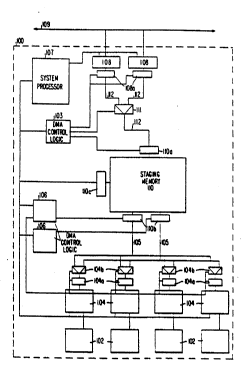
FIG. l shows a mass storage system lO0 that
includes one or more mass storage devices 102 ~e.g.,
disk drives or disk drive arrays) and corresponding
device interfaces 104 for communicating between devices
102 and other circuitry in mass storage system lO0.
Mass storage system lO0 is connected to a network
communication bus 109 via device interfaces 108. There
is provided in mass storage system lO0 a staging memory
llO for temporarily storing information during a data
transfer between the mass storage devices 102 and a
host computer attached to network communication bus
109. This staging memory is used, for example, to hold
data received from one of either device interfaces 104
or 108 pending readiness of another device interface to
receive the data. In the case of a data transfer from
a host computer on network bus lO9 to a mass storage
device 103, the staging memory llO receives the data
from one of device interfaces 108 and holds the data
until it is transferred to one of device interfaces
104. In the case of a data transfer from a mass
storage device 102 to a host computer attached to
network bus lO9, the staging memory llO receives the
data from one of device interfaces 104 and holds the
.
.
WO91/13397 2 0 7 ~ 5 3 ~ PCT/US91/01251
data until it is transferred to one of device
~ interfaces 108. Similarly, staging memory 110 may also
; hold data that is transferred between device interfaces
of like kind (e.g., a transfer from one of device
interface 104 to another of device interface 104).
This same memory may be used for purposes of handling
transfers of information other than mass storage data,
such as command messages between a host computer
connected to network bus 109 and mass storage system
10 100.
Data transfers in mass storage system 100 are
controlled by system processor 107 through DMA control
logic components 103 and 106. DMA control logic
component 103 controls the transfer of data between
lS device interfaces 108 and staging memory 110. DMA
control logic components 106 control the transfer of
data between device interfaces 104 and staging memory
110. In the embodiment of FIG. 1, two device
interfaces 108 are shown connected to staging memory
- 20 110 through a 2:1 multiplexer 111, which in response to
a control signal from DMA logic component 103
determines which of the two device interfaces 108 may
communicate with staging memory 110. Each of device
interfaces 108 includes a port 108a for interfacing
with DMA bus 112. Likewise, staging memory 110
includes a port llOa for interfacing with DMA bus 112.
DMA control logic component 103 provides control
signals to each of ports 108a and llOa and multiplexer
111 to accomplish transfers of data on DMA bus 112.
Each of device interfaces 104 has a port 104a for
transmitting or receiving DMA data on either of two DMA
buses 105 as determined by the setting of corresponding
2:1 multiplexers 104b. The set-up of each of
multiplexers 104b is controlled by two DMA control
logic components 106. Likewise staging memory 110
. ,, -
W O 91/13397 . PC~r/US91/01251 ~076~3~
: - 12 -
"
includes two ports llOb for communicating with a
respective one of DMA buses 105. By providing two DMA
busses 105 between device interfaces 104 and staging
memory 110 each with a separate DMA control logic
component 106, there can be two simultaneous DMA
transfers between staging memory 110 and two different
ones of device interfaces 104. Each of DMA control
logic components 106 provides control signals to ports
104a and llOb and multiplexers 104b to accomplish data
transfers on DMA bus 105. In addition to controlling
DMA logic components 103 and 105, system processor 107
has direct access to staging memory 110 via port llOc.
System processor 107 also has direct access to device
interfaces 104 and 108.
As described in greater detail below, DMA
control logic component 103 serves the purpose of off-
loading data transfer overhead from system processor
107 in connection with a data transfer between staging
memory 110 and one of device interfaces 108 after an
initial set-up of DMA control logic component 103 and
device interface 108. Similarly, also as described in
greater detail below, DMA control logic components 106
serve the purpose of off-loading data transfer overhead
from system processor 107 in connection with a data
transfer between staging memory 110 and one of device
interfaces 104 after an initial set-up of the
appropriate DMA logic components 106.
FIG. 2 shows a block diagram of an exemplary
embodiment of the packet receiving system of the
present invention implemented to receive data packets
from device interfaces 108 into staging memory 110.
Device interfaces 108 receive information over bus 109
in the form of packets, such as the data packet 300
shown in FIG. 3. The format of these packets typically
is defined such that each packet has a known size
,
WO91/133~7 2 ~ 7 ~ S 3 ~ . PCT/US9t/Ot251
- 13 -
usually indicated in the header field defined below.
and includes three fields, including a packet header or
identification field 300a, a data field 300b, and a
field 300c for validation information (e.g., CRC
information). The actual format of the packets may
vary depending on the information processing system in
which the packet receiving system of the present
invention is used. As will be described in greater
detail below, the present invention is capable of
accommodating variations in packet size. It is also to
be appreciated that the format of data packet 300 may
be used to transfer control or status information -
between a computer and the mass storage system, such
that the data field of a packet received by device
- 15 interface l08 may contain information other than mass
storage data, such as control or sta~us information.
In packet 300 of FIG. 3, the type of data contained by
field 300b (e.g., mass storage data, control or status
information) is identified by the OPCODE portion of
identification field 30Oa.
~ Various schemes are used in conventional
information processing systems for referencing
individual packets containing mass storage data. One
such conventional scheme involves transaction-based
packet transfers. Each transaction has a number by
which it and each packet included in the transaction
are referred to. Where a plurality of packets is
included in a particular transaction, the order of tne
mass storage data in the packets is identified by an
offset value equal to the number of words or bytes or
other data in it by which the beginning of the mass
storage data in each packet is offset from the
beginning of the mass storage data in the first packet
in the transaction. A transaction identification field
302 and an offset value field 304 are shown in data
, . . : .: .- :
,,~, . ::
W091/t3397 2 0 7 6 5 3 3 PCT/US91/01251
- 14 -
packet 300 as part of identification field 300a. The
exemplary embodiment of the packet receiving system of
the present invention described herein is discussed in
the context of a network using this type of packet
S reference. As will be apparent to one of skill in the
art, however, embodiments of the present invention can
be practiced with other packet identification schemes.
Moreover, as will also be apparent, the present
invention can be practiced without regard to any
particular destination buffer address that may be
specified in the packet.
Generally, a transfer of packeted data over a
conventional shared system or network bus, such as may
be involved in writing data from the memory of a
central processor to a mass storage system, is
initiated by a command packet from a remote central
processor to the mass storage system. For example, in
a write transaction, the command packet typically
requests the mass storage system to respond by
providing a return packet including, among other
information, a receiving address, a source address ~
(provided to the mass storage system by the requesting
computer) and a transaction identifier. Upon receipt
of this response, the remote central processor places
the data it seeks to transfer into packets, and places
the receiving address and transaction identifier
generated by the mass storage system into the
corresponding fields of each data packet. The central
processor also generates an offset value for each data
packet, and typically transmits the data packets in the
order of their offset value to the mass storage system.
Because of the multiplexing capability of a
packet-switching system, these data packets may be
received by the mass storage system interspersed among
data packets associated with other transactions. In a
:: . ~ : " . :
:: .. , , : , -
207~.~33
WO 91t13397 ~ PCT/US91/01251
- 15 -
typical conventional mass storage system, the data from
the received data packets would be placed in contiguous
: memory locations beginning at the receiving address
identified in the address field of the packets plus any
offset designated in each packet.
The staging memory llO of the present
invention is useful in a mass storage system to allow
received data packets to be stored in memory at non-
contiguous locations unknown even symbolically to the
remote central processor. Staging memory llO comprises
an addressable memory circuit. The memory elements of
staging memory llO may be impiemented using ~~ -
commercially available integrated circuit RAM devices
(e.q., devices such as Motorola's 6293 RAM chip).
Commercially available register devices also may be
used to provide ports llOa, llOb, and llOc. Each port
preferably comprises a data latch register, an address
counter and a read/write enable register, and may
include other logic as may be desired to implement the
port functions. Since the purpose of staging memory
llO is to stage network packets, the memory is
logically divided by system processor 107 into a
plurality of "staging elements" 200, each of which can
be described by an address and a-length. In this
embodiment, all staging elements are of equal length,
that length being the maximum expected packet length.
This logical division is accomplished by system
processor 107 before mass storage system lOO enters an
on-line state. System processor 107 divides the size
of the staging memory llO by the maximum expected
packet length to determine the number of staging
elements 200, and creates a list SE FREE POOL in its
memory of the starting addresses of each staging
element 200.
- '; .' ''; - ,~
'-"'' ''.,., '''~'-' ' ~
WO91/13397 ~ 07~:~ 3 ~ PCT/US91/01251
- 16 -
When a remote central processor initiates a
write operation to mass storage system l00, system
processor 107 generates and returns to the central
processor, as previously described, a packet including
a transaction identifier. System processor 107 also
places the generated transaction identifier into a
memory-resident table for subsequent use, as described
hereafter, in completing outstanding transactions after
data is placed in staging memory ll0. An example of
such a table, described in greater detail below, is
shown in FIG. 4.
Prior to a packet transfer transaction,
system processor 107 programs a sequence storage
circuit 202 in DMA control logic 103 with a series of
staging element identifiers. These identifiers
correspond to individual staging elements of staging
memory ll0 which are available to receive packets.
They are selected by system processor 107 from the
available or currently unused staging elements
identified on the ~E FREE POOL list, and are
individually accessed by port control hardware 203 to
store data packets received by device interfaces 108
into the corresponding staging elements of staging
memory ll0. Port control hardware 203 comprises logic,
which may be conventionally implemented, such as by
using discrete logic or programmable array logic, to
manipulate the control, address, and data registers of
ports 108a and ll0a, and to control multiplexer lll, as
required by the particular implementation of these
circuits for transferring data between device
interfaces 108 and staging memory ll0.
In the embodiment of FIG. 2, the sequence
storage circuit 202 is implemented using a conventional
FIFO (first in first out) storage circuit (labeled RCV
ADDR FIFO) in which staging element identifiers stored
. ~: . , .
: . - . .
WO91/13397 2 0 7 ~ 3 ~ PCT/US91/01251
- 17 -
in the circuit are accessed in the same sequence that
they are loaded by system processor 107. The sequence
in which the programmed identifiers are accessed by
port control hardware 203 can be in a different order
if desired (e.g., the identifiers can be accessed in
reverse order, such as by using a LIFO circuit -- last
in first out). In addition, the sequence storage
circuit can be implemented by circuitry other than a
FIFO or LIFO circuit, such as by using RAM or register
arrays, or a microprocessor.
In a preferred embodiment of the present
invention, each~staging element identifier includes the - -
starting address SE in staging memory 110 of the
corresponding staging element. As each address SE is
loaded by system processor 107 into RCV ADDR FIF0 202,
a short "tag number" RT is joined to the address, and
this tag number and the corresponding starting address
and length of each staging element loaded into
circuit 202 is placed by system processor 107 into a
reference table 204. The purpose of the tag number is
to provide a short hand reference to each starting
address SE loaded into RCV ADDR FIF0 202 for use in
generating status words in RCV STATUS FIFO 206. By
using the tag number instead of the actual starting
address of the stagi~g element in RCV STATUS FIFO 206,
the necessary bit-width of FIF0 206 is kept small. The
generation of the status words in RCV status FIF0 206
is described below.
Tag numbers are loaded into RCV ADDR FIF0 202
in consecutive order, although another order may be
used, as long as the order of tag numbers in RCV ADDR
FIFO 202 is reflected by reference table 204.
Preferably the tag numbers have values from 0 to (m-l),
where m is a parameter variable equal to the depth, or
a portion thereof, of RCV ADDR FIF0 202 (i.e., the
,-i . , . :
'' : ' . ~ .:
-
WO91/13397 2 ~ 3 ~ PCT/US91/01251
- 18
number of staging element identifiers that can be
loaded into RCV ADDR FIFO 202 at one time). For
example, if a FIFO circuit having a depth of 16 or more
staging element identifiers is used, tag number T may
comprise a 4-bit binary number having a value of 0-15.
The first staging element address loaded into RCV ADDR
FIFO 202 might be assigned a tag number of 0, in which
case the second will be assigned 1, etc. In this case,
the tag number acts as a modulo-16 counter, such that
the next tag number used after 15 would be 0.
System processor 107 reloads RCV ADDR FIFO
202 with starting addresses of currently available
staging elements from the SE_FREE_POOL list as the
initially loaded addresses are used by port control
hardware 203 to receive data packets arriving at device
interfaces 108 from bus 109. System processor 107
updates reference table 204 as the system processor
reloads RCV ADDR FIFO 202. Preferably, the initial
loading of staging element identifiers in RCV ADDR FIFO
202 is done when the mass storage system is
initialized. Of course, when a staging element
receives a packet, it becomes unavailable until such
time as that packet is transferred from the staging
element to a mass storage device interface or is
otherwise processed, at which time the staging element
returns to an available state and is returned to the
SE-FREE-POOL list. Thus, during the course of
operation of staging memory 110 individual staging
elements will cycle between available and unavailable
states at various times. System processor 107 keeps
track of this cycling process using the SE-FREE-POOL
list in order to know which staging elements are
available at any given time to load into RCV ADDR
FIFO 202.
: . , ,
: - . ,
WO 91/13397 2 0 ~ ~ ~ 3 3 PCT/US91/01251
-- 19 --
In the preferred embodiment, device interface
108 checks and strips the CRC information (e.g.,
validation field 300c) from ~ackets that it receives
from bus 109, such that a data segment comprising the
header and data fields from each packet received is
stored in staging memory llO. After the data segment
from each data packet is received by staging memory
llO, port control hardware 203 loads a corresponding
status identifier into FIFO circuit 206 (RCV STATUS
FIFO) to indicate completion of the packet transfer.
The status identifier includes a group of STAT bits and
the tag number that''was assigned in RCV ADDR FIFO 202
to the staging element which received the packet. STAT
bits may include, for example, an error bit that
indicates whether or not a transmission error was
detected by the DMA control logic 103 and a bit
indicating which of device interfaces 108 received the
packet from bus lO9. As with the RCV ADDR FIFO 202,
RCV STATUS FIFO 206 can be implemented using
conventional circuitry other than a FIFO circuit.
Upon transition of RCV STATUS FIFO 206 from
an empty to a non-empty state, an interrupt is
generated to system processor 107 to indicate that a
packet has been received. In response to the
interrupt, system processor 107 reads the tag number of
the first status identifier in RCV STATUS FIFO 206 and
determines the starting address and length of the
corresponding staging'element from table 204 (it may
not be necessary to list the lengths of the staging
elements in table 204 if they are all equal, in which
case ~he length may be stored in a single memory
location or register which is read by system processor
107). System processor 107 then places the starting
address, length and offset of the packet into table 400
as shown in FIG. 4. The staging element identifier
WO91/13397 2 0 7 6 5 3 3 PCT/US91/01251
- 20 -
entry in table 204 corresponding to the tag number read
from the RCV STATUS FIFO 206 is set to a null value to
indicate that there is no longer a valid tag by that
number in the DMA control logic 103. Table 400 is
indexed according to the transaction identifiers of
outstanding transactions, such that for a given
transaction identifier, the starting addresses of
staging elements having received data packets
associated with that transaction are listed by syscem
processor 107 in the order in which the packets of that
transaction were received by a device interface 108 or
in the order of their offset. Table 400 is used by
system processor 107 to complete the transfer of data
from staging memory llO to mass storage device
interfaces 104, as described in connection with FIG. 5.
It may be desired that new control
information such as logical block address and mass
storage device number, for internal use by the mass
storage system in completing the transfer to mass
storage, be stored in a staging element with the data
packet. This can be accomplished simply by having
system processor 107 write the new control information
over selected portions of the original control elements
. contained in the header field of the packet after the
2S packet has been placed in staging memory llO.
Alternatively, such new control information can be
added to the packet data field by DMA control logic 106
as the data fields are transferred from staging memory
llO to mass storage device interface 104.
After system processor 107 accesses the first
status identifier in RCV STATUS FIFO 206 in response to
an interNpt and places the address of the associated
staging element into table 400, system processor 107
checks RCV STATUS FIF0 206 for additional status
identifiers, and repeats the accessing process for each
-
:: .- : :
.,
.
WO91/13397 2 ~ ~ 6 5 3 ~ PCTtUS91/01251
- 21 -
such identifier. If there are no more identifiers in
RCV STATUS FIFO 206, system processor 107 returns to
other operations until interrupted again.
Where a packet arriving into device interface
108 is other than a mass storage data packet, such as a
command packet or other type of message, the packet is
identified by system processor 107 as being something
other than mass storage data. The packet is received
into staging memory 110 in the same manner as a mass
storage data packet except that system processor 107
does not place the corresponding staging element
address into table 400. Instsad, system processor 107
provides the staging element address containing the
packet to other software in the control circuitry of
the mass storage syst~m, which in turn processes the
packet and ultimately returns the staging element which
contained the packet to the SE-FREE-POOL.
When this system processor detects that all
mass storage data packets for a particular write
transaction have been received from bus 109, it
prepares to transfer the mass storage data to one of
mass storage device interfaces 104.
FIG. 5 illustrates an exemplary embodiment of
a "snaking/desnaking" mechanism for transferring data
between staging memory 110 and a DMA channel 105
connected to ~ass storage device interfaces 104. The
present invention concerns data transfers in both
directions over DMA channel 105. The term "snaking"
has been previously described herein. First will be
described a method for snaking together data stored in
selected staging elements of staging memory 110 to
transmit the data as a single contiguous DMA data
transfer to one of mass storage device interfaces 104.
For purposes of explanation, it is assumed
that saveral packets of mass storage data associated
,, - ,
' ,. " ,:,
WO91/13397 2 0 7 6 5 3 ~ PCT/US91/01251_
with a single data transfer transaction have been
transmitted by a computer to the mass storage system,
and have been stored in various staging elements 200 of
staging memory llO in accordance with the packet
receiving aspect of the present invention described in
connection with FIG. 2. The stored mass storage data
pacXets are of equal length, with the possible
exception of the last data segment associated with the
transaction, which may have only a fractional amount of
mass storage data. Each stored mass storage data
packet is modified by system processor 107 to include a
header comprising control and addressing information
for use in directing the corresponding mass storage
data to a particular logical or physical location in
mass storage (as previously stated, this information
may be written over the control information originally
included in the header field of the packet). It is
also assumed that system processor 107 has knowledge of
the starting memory addresses, lengths and offset
values of the data segments to be snaked together.
This can be accomplished, for example, by creating a
look-up data table like that shown in FIG. 4 when the
data is stored in staging memory llO, in the manner
previously described.
To transfer the data segments from selected
staging elements 200 of staging memory llO to DMA
channel 105, system processor 107 programs sequence
storage circuit 504 of DMA control logic 106 with a
series of memory addresses ("SE ADDRESS") corresponding
to the starting addresses in memory of the modified
header fields contained in each of the selected staging
elements. Sequence storage circuit 504 is preferably
implemented using a FIF0 storage circuit (labeled
"SNAKE/DESNAKE FIF0") in which staging memory addresses
are programmed and accessed in accordance with the
. . . ~ :. :
::, . . . - . .
W09t/13397 ~0~ &~33 PCT/US91/Ot251
- 23 -
offset values of the data segments contained in the
corresponding staging elements. The sequence in which
the staging memory addresses are programmed (and thus
the sequence in which the contents of corresponding
staging elements are transferred) can be varied as
desired. Sequence storage circuit 504 may be
implemented by circuitry other than a FIFO circuit,
such as by using a LIFO circuit, RAM or register
arrays, or a microprocessor.
After programming sequence storage circuit
504, system processor 107 loads data transfer length
counter 510 with a value equal to the total length of -
data to be transferred. This loading of data transfer
length counter 510 initiates the operation of port
control hardware 506. Port control hardware 506
comprises a state machine sequence circuit and other
logic, which may be conventionally implemented, such as
by using discrete logic or programmable array logic, to
manipulate the control address and data registers of
parts 104a and llOb, and to control multiplexer 104b,
and may be constructed in any conventional manner to
perform the DMA transfer without requiring further
attention from system processor 107. A flow diagram
600 illustrating the states of the state sequence
circuit of port control hardware 506 as it executes DMA
transfers between staging memory 110 and DMA channel
105 is shown in FIG. 6.
The states involved in à transfer from
staging memory 110 to device interface 104 are shown in
the lower portion of FIG. 6, and are generally referred
to herein as read sequence 600a. ~he state machine
sequence circuit of port control hardware 506 begins
read sequence 600a from an idle state 601 when state
machine sequence circuit 506 is initiated by system
processor 107 with the loading of data transfer length
-... . ,:
WO 91/13397 2 ~7 ~ ~ 3 3 PCT/US91/01251
.
- 24
counter 510. The state machine sequence circuit first
loads block length counter 508 with a value equal to
the length of each header/data segment (e.g., 520
bytes) in staging memory 110 (excepting fractional data
segments) (state 602). The state machine sequence
circuit next causes the port control hardware to
generate any control signals that may be necessary to
set up DMA channel 105, mass storage device interface
port 104a and staging memory port llOb for the DMA
transfer (state 604).
The state machine sequence circuit of port
control hardware 506 then assembles the selected data
segments into a single data stream 512 which is
transferred over DMA channel 105 to mass storage device
interface 104. This may be accomplished as follows.
The state machine sequence circuit causes the first
staging memory address in sequence storage circuit 504
to be loaded into address counter 509, which provides
staging memory port llOb with staging element addresses
for directing header/data bytes out of staging memory
110 (state 606). Header 514 and~data field 516,
comprising a header/data segment 517, are then
transferred from the addressed staging element to DMA
channel 105.
After each byte is transferred to DMA channel
105, block length counter 508 and data transfer length
counter 510 are each decremented by one. Although
transfers between staging memory 110 and DMA channel
105 are described herein as taking place one byte at a
time, such that block length counter 508 and data
transfer length counter 510 are decremented on a byte-
by-byte basis, the ports llOb and 104a and DMA channel
105 may be implemented to transfer larger amounts of
data in parallel (e.g., longwords). In such case,
counters 508 and 510 may be implemented to count
-
: . : .- ~: ~ ~
: . .
WO91/13397 PCT/US91/01251
2o~533
- 25 -
longwords or other units rather than bytes. When block
length counter 508 reaches zero, indicating that a full
header/data segment 517 of 520 bytes has been
transferred to DMA channel 105, the state machine
sequence circuit directs port control hardware 506 to
reload block length counter 508 with the header/data
segment length value and to cause the next staging
memory address to be loaded into address counter 509
from sequence storage circuit 504 to begin the transfer
of another header/data segment (state 608). Before
transfer of this next header/data segment begins, the
state machine sequence circuit of port control hardware
506 causes data validation information ("CRC" 518) to
be appended to data field 516 of the first segment in
DMA data stream 512 (state 610). This process (states
606, 608, 610) is repeated until data transfer length
counter 510 equals one. If block length counter 508
equals one when data transfer counter 510 reaches one,
the last byte of data is transferred and each counter
is decremented to zero (state 612). A data validation
field is then appended to the just transferred data
field (state 614) and the state machine sequence
circuit 506 returns to the idle state 601. If block
length counter 508 is not equal to one when data
transfer length counter 510 equals one (i.e., when the
last data byte stored in staging memory 110 is being
transferred), block length counter 508 will have a non-
zero value after the last stored data byte has been
transferred and counters 508 and 510 have been
decremented. To complete the last data field of DMA
data stream 512 the state machine sequence circuit
causes port control hardware 506 to continue
transferring bytes of "pad" data on bus 105 as part of
the data stream (state 616). This "pad" data comprises
a repeating value known as the pad byte. Pad bytes are
.,, ~ .
:. ~. ~';: ' ' .
WO91/13397 PCT/US91/01251
2~76533
- 26 -
transferred until the length of the last transmitted
header/data segment is equal to the lengths of the
previous header/data segments. This is accomplished by
decrementing the block length counter after each pad
byte is transmitted, and by continuing the padding
operation until the block length counter reaches zero.
After the last pad byte is transferred and the block
length counter is decremented to zero (state 618), a
data validation field is transmitted (state 614) to
complete the DMA data stream from staging memory 110 to
device interface 104.
With respect to a data transfer in which a
remote central processor on network bus 109 seeks to
retrieve data from mass storage 102 (i.e., a read mass
storage data operation), mechanisms similar to those
described above can be used to route header/data
segments 517 from a single contiguous DMA da~a stream
512 on DMA channel 105 into available staging elements
of staging memory 110, and to then transfer the
header/data segments in pacXet form from staging memory
110 to network communication bus 109 via device
interface 108.
The read operation is initiated by a command
packet from the remote central processor that provides,
among other information, an identification of the mass
storage data to be read. The command packet is
received by mass storage system 100 via a network bus
device interface 108 and is transferred to staging
memory 110 in the manner previously described. System
processor 107 reads the command packet stored in
staging memory 110, and assigns one or more transaction
identification numbers to the command. The number of
transaction identification numbers used depends on the
amount of data requested. System processor 107 then
enters the transaction identification numbers into
:
. -
207~533
WO9t/13397 PCT/US91/01251
table 400, and notifies the appropriate mass storage
device 102 to retrieve the data requested by the
command packet.
When the mass storage device 102 is ready to
transfer the data associated with a particular
transaction identification number, the mass storage
device notifies its device interface 104 which in turn
causes system processor 107 to be interrupted. System
processor 107 determines how many staging elements of
staging memory 110 would be required to transfer the
mass storage data associated with the transaction
identification number and obtains the necessary number
of staging elements from the SE FREE POOL list. For
each stagin7 element, the address in staging memory 110
at which transfer of the header/data segment is to
begin is loaded into SNA Æ/DESNAÆ FIFO 504. The
staging element addresses are also entered into table
400 in the order in which they are loaded into FIFO
504.
System processor then selects an available
DMA channel 105, and initiates the operation of the
state machine sequence circuit within the DMA control
logic component 106 associated with the selected
channel. Referring now to the states of write (to
25 staging memory 110) sequence 600b, the operation of the
state machine sequence circuit is initiated by system
processor 107 by loading data transfer length counter
510 with a value equal to the total length of data to
be transferred (state 620). The state machine sequence
circuit then causes port control hardware 506 to
generate any control signals that may be necessary to
condition DMA channel 105 and port 110b of staging
memory 110 for the DMA transfer (state 622), and loads
block length counter 508 with a value equal to the
., . . ~
'
-. . ~ ,
' .' : ~ ' ,' ''
WO91/t3397 PCT/US91/01251
2 ~ 7 6 ~
- 28 -
length of each header/data segment 517 to be
transferred (state 624).
The state machine sequence circuit of port
control hardware 506 next causes the first staging
memory address in the sequence storage circuit 504 to
be loaded into address counter 509, which provides
staging memory port llOb with staging element addresses
for directing header/data bytes into staging memory llo
(state 624). A header/data segment 517 is then
transferred from mass storage device interface port
104a to the addressed staging element. After each byte
is transferred to the staging element, block length
counter 508 and data transfer length counter 510 are
decremented by one. When a full header/data segment
517 has been transferred to staging memorv 110 (state
626), as indicated by block length counter 508 being
decremented from one to zero, the state machine
sequence circuit of port control hardware 506 checks
the data validation field appended to the end of the
header/data segment to ensure that the header/data
segment was not corrupted during the transfer (state
628). The data validation informatior. is not
necessarily stored in staging memory 110, but can be
stripped from the header/data segment when checked by
the state machine sequence circuit of port control
hardware 506. If stripped, new validation information
is appended when the header/data segment is later
transferred out of staging memory 110. If the state
machine sequence circuit of port control hardware 506
detects an error when the data validation information
is checked, an interrupt is posted to the system
processor 107.
After the data validation information is
checked and it is determined that the header/data
segment is valid, the state machine sequence circuit
- -- : . :
: , . : :.
:: ~. : - . ,
- . : : ~ ~ : .'
, ,,
.:
WO91/13397 2 0 7 6 ~ 3 3 PCT/US91/01251
.:`
- 29 -
directs the port control hardware to reload block
length counter 508 with the header/data segment length
value and to cause the next staging memory address from
the SNAKE/DESNAKE FIF0 504 to be loaded into address
counter 509 to begin the transfer of another
header/data segment. This process is repeated until
the last data byte of the data stream on DMA channel
105 is transferred. When block length counter 508
decrements from one to zero after the last data byte is
transferred (state 630), the state machine sequence
circuit checks and strips the last data validation
field (state 632) and returns to idle state 601.
After the last byte of data is transferred to
staging memory 110, DMA control logic 106 interrupts
system processor 107 to tell the processor that the
transfer of data associated with a transaction
identification number has been completed. System
processor 107 verifies that the header fields of the
header/data segments stored in staging memory 110
indicate that the correct mass storage data has been
transferred. System processor 107 then writes new
header fields on the stored header/data segments to
meet network addressing format requirements, and
prepares to transfer the header/data segments to one of
device interfaces 108 for transmission in packet form
on bus 109.
FIG. 7 illustrates the transfer of data from
staging memory 110 to a network bus device interface
108. Prior to transfer, system processor 107 selects
one of the two device interfaces 108 and programs the
corresponding sequence storage circuit 702a or 702b
(labeled TMT ADDR FIF0) with a series of staging
element identifiers and enters the staging element
addresses and lengths into a corresponding table 705a
or 705b. These identifiers correspond to individual
..
- . , . ,: ,~, ,
WO91/13397 - PCT/US9t/01251
207~3~
- 30 -
staging elements of staging memory 110 that contain
data to be transmitted to device interface 108. This
sequence is obtained from an entry in table 400
generated during the transfer of data from mass storage
device interfaces 104 to staging memory 110. For
purposes of illustration, it is assumed hereafter that
the device interface for a cable A has been selected by
system processor 107. Each identifier preferably
comprises the starting memory address of the rewritten
header field stored in the corresponding staging
_ element and a tag number TA.
After programming TMT ADDR FIFO 702a, system
processor 107 directs the port control hardware 706 of
DMA control logic 103 to access the first staging
element identifier from TMT ADDR FIFO 702a and to
transfer the pac~et stored in the corresponding staging
element to device interface 108. System processor 107
is then free for other processes. DMA control logic
103 repeats the process for each identifier in TMT ADDR
FIFO 702a. After each packet is transmitted to device
interface 108, DMA control logic 103 loads a
corresponding status identifier into FIFO circuit 704a
(labeled TMT STATUS FIF0). Here, the status identifier
may be expanded to include, in addition to the status
bits previously discussed in connection with RCV STATUS
FIFO 206, counts of any unsuccessful attempts to
transmit. Upon transition of TMT STATUS FIFO 704a from
an empty state to a non-empty state, an interrupt to
system processor 107 is generated to indicate that a
packet has been transferred. System processor 107
checks the status of the transfer of the first packet
to device interface 108, and then looks for additional
status identifiers. If the status indicates a
successful transfer, the entry in table 705a
corresponding to the tag number read from the RCV
- - .. ,:. :
: : . . .-
. .: .. ~ ,,~ . . :
` ` . . ' . ~ ~ ~ , . r
.
W O 91/13397 2 0 ~ ~ ~ 3 ~ P(~r/US91/01251
- 31 -
STATUS FIFO 704a is set to a null value. After
checking any additional status identifiers in TMT
STATUS FIF0 702a, system processor 107 returns to other
operations until interrupted again.
It may be desired that data be transferred
between staging memory 110 and mass storage device
interfaces 104 in header/data segments having a
different length than that of the header and data
fields of the packets received from bus 109. It may
also be that the lengths of the header and data fields
----of-the-packets and/or the lengths of header/data
segments transferred between staging memory 110 and
mass storage device interfaces 104 vary from one to
another. In either case, the differences in length can
be accommodated by defining the length of staging
elements in staging memory 110 to be a variable
parameter. In so doing, the variable length of
individual staging elements must be taken into account
when transferring data to and from staging memory 110.
For example, FIG. 8 illustrates an
alternative embodiment of the snaking/desnaking system
of FIG. 5, in which staging element identifiers include
a staging element length parameter that is loaded into
FIFO 804 along with a corresponding staging memory
element address. An additional counter circuit 802
(labeled SE LENGTH CNT~) is provided, into which the
staging element length value from FIFO 804 is loaded
after the corresponding staging element address is
loaded by the port control hardware 806 into the
address counter 509. The value of counter 802 is
decremented once for each byte of the header/data
segment 517 transferred to or from staging memory 110,
and is used instead of the value of block length
counter 508 to determine when port control hardware 506
is to fetch the next staging element address and length
~; i
: :
,: : . ,~
WO91/13397 2 ~ ~ 6 ~ 3 3 PCT/US91/01251
from FIFO 804. Block length counter 508 still
determines when port control hardware 506 is to insert
data validation information ("CRC")`into the data
stream on DMA channel 105, and padding is carried out
in the same manner as previously described.
The use of a staging element length parameter
as illustrated in FIG. 8 thus permits the length of the
header/data fields of the data transferred between
staging memory 110 and mass storage device interfaces
104 to be independent of the length of packets received
by mass storage system 100. _
Thus a novel method and apparatus for
transferring data through a staging memory has been
described. One skilled in the art will appreciate that
the present invention can be practiced by other than
the described embodiments, and in particular may be
incorporated in circuits other than the described mass
storage system. The described embodiment is presented
for purposes of illustration and not of limitation, and
the present invention is limited only by the claims
which follow.
- : .. ,. . . ~.
- -::.: :.:: :. : . .
. . . ,: ~ , . .
,
.- . : . .. : ~ ,
, .. : ,: .~ .. . ~ ::