Note: Descriptions are shown in the official language in which they were submitted.
2~7~72~
DC Te~mination Clrcult for 2BlQ ISDN
Basic Rate Physical Layer Line Code Protocol
Background of the Inventio~
The pr~sent invention relates to DC termination
circuits and more specifically to a DC termination
circuit having a bi-lateral switch for use in telephone
equipment meeting 2BlQ specifications.
~ elephone campanies may provide many different types
of services to subs¢ribers. These services may be
analog, known as POTS (Plain Old Telephone Service) or
digital of whi~h there are numerous types. When ISDN
(IntPgrated Services Diyital Network) was first proposed,
e~uipment manufacturers in the United States developed
their own ideas for implementing two wire, full duplex,
relatively high speed data communications over a local
telephone loop. AT~T and Northern Telecomm each
developed a priority ISDN implementation for the "U"
interface re~erence point called AMI (Alternating Mark
Inversion). These and other proposed ISDN
implementations were submitted to the American National
Standards ~nstitute (ANSI), which developed its own ISDN
standard for the "U" int~rface reference point called
2BlQ (2 Binary, 1 Quaternary Modulation~. 2BlQ has now
been adapted as the ISDN standard for the United State~.
Each type of telephone service has a DC termination
requirement. The DC termination is used, among other
things, for making a low level DC current in the loop to
prevent contact plating and oxidation of all the various
connection points between the phone switch and the phone.
Switching equipment in c ntral o~ices of telephone
companies ha~e the capability of testing a subscriber's
loop to determine the type of service the subscriber has,
analog or digital, and if it is digital the kind o~
digital ~ervic~ it has. Metallic loop testers in the
phon2 switch capitalize on the DC termination
2~7~7~
characteristics of the subscriber's equipment to
determine the type of service in place. A requirement of
this type of loop tast i5 that it can be performed on un-
powered subscriber's equipment.
All digital service standards have a characteristic
response to a test from the central office. One o~ the
characteristics of all digital service standards is the
DC termination of the equipment being tested. In the
case of the A~&T ' s A~I service, the DC termination or
load circuit is a re~istor and diode in seriss. The DC
termination circuit ln the 2BlQ serv.ice embodies a bi-
lateral switch that is normally o~f. A sweep voltage is
applied to the loop from a central of~ice switch, which
activates the DC termination circuit. Knowing that the
2B1~ DC termination is the only type of digital ser~ice
that embodies a bi-lateral switch, the switch in the
central office can determine the loop service is 2BlQ by
the respon~e from the loop.
Con~entional circuits have be~n designed to
implement the 2BlQ standard, but have used physically
large componPnts due to the high power dissipation o~ the
circuit designs. What is needed is a DC termination
circuit that meets the 2BlQ standard for termination
response while at the same time minimizing the power
dissipat~.d by the circuit.
Summary of the Inve~tio~
Accordingly the present invention is a DC
terminakion circuit for implementing the 2BlQ standard
for ISDN basic rate physical layer line code protocol
having a full-wave bridge rectifier for receiving a DC
voltage ~rom an external signal source and generating a
constant polarity DC output voltage. A hold-up current
source is coupled to the output of the bridgP rectifier
for maintaining circuit operation during momentary loss
of the externally applied voltage. A trigger circuit is
:: .
,. . .
2~7~72~
coupled to receive the DC ~oltage for coupling a low DC
: impedance, low power dissipation load to the external
; signal sourca. A current sink is coupled to the trigger
circuit and the output of the bridge rectifier for
providing the low DC impedance, low power dissipation
load to the external signal source.
A further embodiment of the present invention
provides a means for further reducing the power
dissipation by the low impedance load as a ~unction of
externally applied DC voltage increasing beyond a
predetermined value.
. ~
: The ob~ects, advantages and novel features of the present invention are apparent from the Iollowing
detailed description when read in conjunction with
appended claims and attached drawings.
Brief de criptio~ of th~ ~rawing~
Fig. 1 is a block diagram o~ the circuit for
producing 2BlQ termination characteristics according to
the present invention~
FigO Z is a block diagram of the circuit for
producing 2BlQ termlnation characteristics in response to
an externally applied voltage from a phone switch
;: according to the present invention.
Flg. 3 is a schematic diagram of the circuit for
producing 2BlQ termination characteristics in response to
an externally applied voltage from a phone switch
according to the present invention.
Fig. 4 is a current vs voltage template showing the
parameters for ~ 2BlQ DC termination circuit.
2~7~72~
Fig, 5 is a bloc~ diagram of a further e~bQdiment of
the DC termination circuit according to the present
`~ invention.
: Fig. 6 is a schematic diagram of the further
embodiment of the DC termination circuit according to the
`;~ present invention.
'~
~ Detailed De~ariptio~ o~ t~e Preferred E~bodima~t
"~
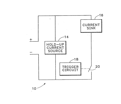
Referring to Fig. 1, there is shown a block diagra~
: of a circuit 10 for producing 2BlQ termination
characteristics. A variable dire~.t current, DC, voltaye
from an external signal source, not shown, having a
: constant polarity is applied to a hold-up current source
14. The Yariable DC voltage is also applied to a current
sink 16 and a trigger circuit 18. The trigger circl~it 18
includes a switch 2 a connected in parallel with the
trigger circuit 18. The trigg~r circuit 18 produces a
trigger signal that acti~ates switch 20 when the variable
DC voltage reaches a predetermined threshold value. With
switch 20 closed, the current sink presents a low DC
impedance, low power dissipation load to the external
signal source. The closing of switch 20 al50 effectively
shunts the trigger circuit 18 from the external signal
source. Alternately, the trigger circuit 18 may be
con~ected in parallel with the series connected current
sink 16 and switch 20, but power dissipation will be
higher.
The block diagra~ o~ Fig. 2 shows the DC termination
circuit 10 ~or implementing the 2BlQ standard for ISDN
basic rate physical layer lin2 code pxotocol, ANSI
specification Tl.601/1988 (draft revision 1/9/1991). A
DC voltag~ from a telephone company central office phone
switch, acting as the ext~rnal signal source, is applied
: to inpu~ terminal~ 22 of a bridge rectifier 12. T~e
polarity of the DC voltage from the phone switch may be
reversed and the bridge rectifier 12 is able to respond
to the different polarity of DC voltage and generate a
constant polarity output voltage. A hold-up current
source 14 is coupled to the output o~ the bridge
rectifier 12 for maintaining circuit operation during
momentary loss of the externally applied DC voltage. A
current sink 16 and trigger circuit 18 are series
connected to the output o~ the bridge rectifier 12 and
connected in parallel with the hold~up current source 14.
A shunt switch 20 is connected in parallel across the
trigger circuit 18.
~ he DC termination circuit 10 acts as a bilateral
switch. In the OFF state the circuit 10 presents a high
impedance to the central office switch while in the ON
state it presents a low impedance. In the preferred
embodiment, the impedance in the OFF state is in megohms
as opposed to an impedance of thousands of ohms in the o~
state. A ra~ping DC voltage is applied to terminals 22
of the bridge rectifier 12 from a central office switch
during a loop test. The bridge rectifier 12 receives the
DC voltage and generates a constant polarity output
voltage. The voltage output from the bridge rectifier 12
is coupled to the hold up current source 14, the current
sink 16 ! and the trigger circuit 18. ~en the ramping
voltage reaches the threshold voltage of the trigger
circuit 18, the trigger circuit 18 turns on closing
switch 20~ This effectively shorts ths trigger circuit
18 from the DC termination circuit 10 while at the same
time coupling the low impedance current sink 16 into the
circuit 10. Shorting the trigger circuit 18 from circuit
10 during the ON state reduces th~ amoun~ of power
dissipated by the DC termination circuit 10. Once switch
20 is closed a~y momentary loss of the input DC voltage
is compen~ated for by the hold-up current source 14. As
the input voltage increases, current through the current
2~7~
sink 16 increase~ by only a ver~ small amount causing the
power dissipated by the circuit to incxease only as a
function of the input voltage. As the voltage deceases
below a predetermined value the current through the
current sink 16 starts to drop. When the current drops
below a predetexmined value, the trigger circuit 18 turns
off and the switch 20 opens, thus placing the DC
termination circuit 10 in its preactivation high
impedance mode.
The 2BlQ DC termination circuit 10 is described in
greater detail in relation to the schematic diagram of
Fig. 3 and the tPmplate of Fig. 4 showing current ~s
voltage levels for 2BlQ DC termination circuits. The
scale for the current value I~ is logarithmic and the
voltage scale is linear. The template shows that in the
OFF state the leakage currPnt IL~ is less than or equal to
5 microamps for voltages less than 20 volts and less than
or equal to 1 milliamp while the voltage across the DC
termination circuit 10 is less than the active~non-activ~
voltage V~. The DC termination circuit 10 transitions to
the ON state when the active/non-active voltage V~ is
between 30 an~ 39 volts. Activation time for V~ i5 in
the range of 3 to 50 milliseconds. The transition from
the OFF state to the ON state must be completed within 50
mil}iseconds from the point where the applied voltage
across the DC termination circuit 10 first exceeds V~.
Application of a voltage greater than V~ for a duration
of less than 3 millisecsnds does not transition the DC
termination circuit 10 to the ON stat2. While in the ON
state, when the voltage acros~ the DC te~mination circuit
10 is 15 volts, the current is greater than or equal to
20 milliampsO The termination circuit 10 rPmains in the
ON state as long as the current is greater than the
threshold hold/release current I~ whose value is in the
range of .1 to 1 milliamps. Application of 9o volts
. ::
.
, ~ ~ '. ' -
..
2~7~72~
through 200 to 400 ohms for a maximum duration of 2
seconds results in a current greatex than 9 milliamps.
The DC termination circuit 10 transitions to the OFF
state when the current falls below the threshold
hold/release current I!iR for a duration greater than the
guaranteed release time of 100 milliseconds. The
transition from the ON state to the OFF state is
completed within 100 milliseconds from the point where
the current first falls 1: elow I~R. The DC termination
circuit 10 does not transition to the OFF state when the
current falls below I~R for less than 3 milliseconds.
~ he bridge rectifier 12, shown in Fig. 3, recei-ves
the test voltage from the central office switch, not
shown, and provides a polarity guard function, assuring
proper application of the test voltage to the rest of the
circuit lO. Capacitor 30 coupled ko the output of the
bridge rectif ier 12 charges to the applled voltage to
provide a te~porary energy source in the case of a
momentary loss of the test voltage. Zenex diode 32
having a brea}cdown voltage o~ 22 volts and series
connected resistor 34 are coupled in parallel with the
capacitor 30 to provide a discharge path for the
capacitor 30 when subjected to the application of an
invalid test Yoltage or other foreign test voltage. As
the test voltage increases beyond the threshold voltage
of the trigger circuit 18, in this case 30 volts, zQner
diode 36 starts conducting in the revers~ breakdown mode.
The c-trrent through the zener diode 36 activakes silicon
controlled rectifier (SCR) 38 acting as a switch. With
SCR 38 latched on, the trigger circuit 18 is effectively
shorted out of t~e DC termination circuit lO. Capacitor
40 and the voltage divider made of resistors 42 and 44 on
the gate of SCR 38 prevent false or early triggering of
the trigger circuit 1~. Resistor5 42 and 44 are also
used to set the trigger voltage at some point above the
?
,:.
,~ 8 2~7~72
zener 36 breakover voltage and to program the
hold/release current I~.
With SCR 38 latched, current sink 16 made of
transistors 46 and 48 is activated maintaining a minimum
constant current therethrough as required by the ANSI
T1.601-1988 specifications. A single bi-polar transistor
with higher power dissipation may equally be used in the
current sink 16 instead of the two transistors 46 and 48
shown. The minimum constant curxent throu~h transistors
46 and 48 is de~ined by zener dlode 50 and resistor 52.
Zener diode 50 has a breakdown voltage o~ 6.2 volts and
effectively clamps the voltage across resistor 52 at this
value less the diode drop of the base-emitter junction of
the transistors 46 and 4~. Resistor 54 is connected
between the ~ terminal of the bridge rectifier 12 and the
bases of transistors 46 and 48 to provide biasing current
to the bases of transistors 46 and 48. Ballast resistors
56 and 58 are connected between the respective emitters
of transistors 46 and 48 and resistor 52 to ensur~ that
the transistors 46 and 48 share power equally. The
values of resistors 56 and 58 are selected to be very
small in comparison to resistor 52 so that zener diode 50
and resistor 52 set the current.
The application of a test voltage from a central
office switch causes capacitor 30 to start charging. As
previousIy stated, the specification calls for a DC
leakage current in the OFF state of less than or equal to
5 microamps for steady state voltages of less than or
equal to 2Q v~lts. Above 20 volts i~ the OFF ~tate the
~C leaka~e current may not exceed 1 milliamp. Zener
dioda 32 breaks down at 22 volts establishing a current
path through the zener 32 and resistor 34 providing a
discharge path ~or capacitor 30 while the DC terminati~n
circuit 10 is in the OFF state. ~hen the test voltage
reache 30 volts, zener diode 36 in the trigger circuit
: ::
9 ~1~7672~
18 breaks down causing current to ~low in SCR gate 38.
In the preferred embodiment, it takes approximately 200
microamps of current through SCR 38 to activate it. The
input voltage at this point is approximately 32-33 volts,
With SCR 38 latched on, current flows through current
sink 16 placing the DC termination circuit in the ON
state. While in the ON state the DC termination circuit
10 acts as a low impedance load to the test voltage.
When the DC termination circuit 10 switches to the ON
state the test voltags may drop down to a lower voltage.
The 2BlQ specification states that in the ON state the
current must ~e greater than or equal to 20 milliamps for
a voltage oX 15 volts. Zener diode 50 breaks down a~ 6.2
volts and ef~ectively clamps the voltage across resistor
52 at 6.2 volts less the diode drop of base emitter
junctions of transistors 46 and 48. The value of
resistor 52 is selected to meet the 20 milliamp/15 volts
specification. Further increas~s in the test voltage
will produce very little change in the current ~low
through current sink 16.
As the test voltage decreases, there comes a point
when the current through the current sink starts to drop.
When the current reaches tAe release current I~ defined
as being between .1 and 1 milliamp, the SCR gate 38 shuts
off and the DC termination circuit transitions to the OFF
state. Cap~citor 30 acts as a hold-up curr~nt source for
I~ in the transition region in case the test voltage
momentarily drop~ due to noise or the like.
Re~erring to Fig. 5, there i5 shown a block diagram
of a fur~her e~bodiment of the DC termination circuit 10
of the present invention. ~e~erring bac~ to the template
of Fig. 4, it shows that above 54 volts the current is
greater than 9 milliamps. It further show~ that at
voltages below 54 volts the minimum current through the
current sink 20 milliamps~ Since the power dissipated by
2~7~2g3
the circuit is a ~unction of the amount of current
flowing in it, it is desirable to reduce the current
through the circuit to the minimum allowable under the
2BlQ specifications to further reduce power dissipated by
the DC termination circuit 10. This is accomplished by
adding a fold-back current limiter 60 to the DC
te~mination circuit 10. As the voltage increases past 5~
volts, the fold-back current limiter 60 effectively shuts
off the current sink 16 and Frovides an alternate current
path in the DC texmination circuit 10 that generates a
current of at least 9 milliamps.
The schematic diagram of Fig. 6, where like elements
of the previous schematic diagram are the same, shows the
fold-back current limiter 60. Below 54 volts the circ~it
operates as previously described with the fold-back
current limiter shut off. As the test voltage passes 51
volts zener diode 62 breaks down and starts conducting.
A voltage divider made of resistors 64 and 66 provide a
voltage bias to the gate of field ef~ect transistor (FET)
68. At approxim~tely 54 volts the voltage bias on the
gate of FET 68 is large enough to cause FET 68 to
conduct. With FET 6a conducting~ a voltag2 divider
network is esta~lished by resistors 70 and 72. A bias
current is provided to the base of transistor 74 by the
voltage divider network, which causes transistor 74 to
conduct~ With transistor 74 conducting, a current path
is established through transistor 74 and resistors 76 and
54 for drawing current away from the base of the current
sink transistor 46 and zener diode 50, which shut down~
The majority of current flows through resistor 70
providing at least 9 milliamps but less than 20 milliamps
of current for the DC termination circuit 10 when the
test voltage equals or ~xceeds 54 volts.
When the test voltage decreases below 54 volts, FET
68 shuts off, which shut~ off transistor 74. With
2~7~72~
11
transis~or 74 shut off, c~rrent again flow5 into the base
of transistor ~6 and through zener 50, which begin to
conduct and reestabllsh the constant current through the
current sink 16.
A DC termination circuit has been described that
implements the new U.S. standard for ISDN basic rate
physical layer line code protocol 2BlQ voltage/current
specifications. The DC terminati4n functlons as a
bilateral switch that pre5ents a high impedance load to a
signal source in the OFF state and a low impedance load
in the ON state. The DC termination circuit has a bridge
rectifier that provides a constant polarity DC output to
the DC termination circuit. A hold-up current source is
connected to the output of the bridge rectifier to
maintain circuit operation during momentary losses of the
t~st signal. A trigger circuit is provided that triggers
a switch when the test voltage passes a threshold voltage
level. The ~witch i~ in parallel with the trigger
circuit so that when the switch is activated, the trigger-
circuit is effecti~ely shorted out of the circuit.
Activation of the switch connects a low impedance, lo~
power dissipation constant current sink to the DC
termination circuit. A further embodiment of the
inventinn is a fol~-back current limiter that shuts of
the current sink and reduces the amount of current
flowing through the DC termination circuit. These and
other aspects of the present invention are set forth in
the appended claims.
~'
.
'~