Note: Descriptions are shown in the official language in which they were submitted.
'~ -
CHARGED AREA (CAD) IMAGE LOSS CONTROL IN A
TRI-LEVEL IMAGING APPARATUS
CROSS-REFERENCES TO RELATED PATENTS
U.S. Patent No. 5157441 issued 10/20/92 and assigned to the
same assignee as the instant application relates to a single pass tri-level
imaging apparatus and method. Compensation for the effects of dark
decay on the background voltage, VmOd, and the toner patch, Vtc readings is
provided using two ESVs (ESV1 and ESV2), the former located prior to the
color or DAD housing and the latter after it. Since the CAD and black toner
patch voltages are measured (using ESV2) after dark decay and CAD
voltage loss have occurred, no compensation for these readings is required.
The DAD image voltage suffers little dark decay change over the life of the
P/R so the average dark decay can be built into the voltage target.
U.S. Patent No. 5212029 issued 05/18/93 and assigned to the
same assignee as the instant application relates to toner patch generation
for use in tri-level imaging which is effected using a laser ROS. Two toner
patches are formed using a single toner patch generator of the type
commonly used in the prior art. The patch generator, used by itself serves
to form one toner patch latent image and together with the ROS exposure
device of the imaging apparatus is used to form the other toner patch latent
mage.
U.S. Patent No. 5227270 issued 07/13/93 and assigned to the
same assignee as the instant application relates to a single pass tri-level
imaging apparatus, wherein a pair of Electrostatic Voltmeters (ESV) are
utilized to monitor various control patch voltages to allow for feedback
control of Infra-Red Densitometer (IRD) readings.
The ESV readings are used to adjust the IRD readings of each toner
patch. For the black toner patch, readings of an ESV positioned between
two developer housing structures are used to monitor the patch voltage. If
the voltage is above target (high development field) the IRD
.,
7 ~ ~
reading is increased by an amount proportional to the voltage error. For the
color toner patch, readings using an ESV positioned upstream of the
developer housing structures and the dark decay projection to the color
housing are used to make a similar correction to the color toner patch IRD
readings (but opposite in sign because, for color, a lower voltage results in
a higher development field).
Canadian Patent application No. 2076846 filed August 25, 1992,
and assigned to the same assignee as the instant application relates to
toner dispensing rate adjustment wherein the Infra-Red Densitometer (IRD)
readings of developed toner patches in a tri-level imaging apparatus are
compared to target values stored in Non-Volatile Memory (NVM) and are
also compared to the previous IRD reading. Toner dispensing decisions (i.e.
addition or reduction) are based on both comparisons. In this manner, not
only are IRD readings examined as to how far the reading is from the target,
they are examined as to current trend (i.e. whether the reading is moving
away from or toward the target).
U.S. Patent No. 5223897 issued 06/20/93 and assigned to the
same assignee as the instant application relates to a tri-level imaging
apparatus wherein two sets of targets, one for use during cycle up
convergence of electrostatics and one during runtime enable single pass
cleaning of developed patches, during cycle up convergence. To this end,
different targets from those used during runtime are used for the preclean,
transfer and pretransfer dicorotrons during cycle up.
Proper charging of the photoreceptor during runtime and cycle up
convergence is also enabled by the provision of two charging targets, one
for each mode of operation.
U.S. Patent No. 5208632 issued 06129193 and assigned to the same
assignee as the instant application relates to cycle up convergence of
electrostatics in a tri-level imaging apparatus wherein cycle up convergence
is shortened through the use of an image output terminal (IOT) resident
image (on a pixel or control board) to obtain charge, discharge and
background voltage readings on every pitch.
U.S. Patent No. 5138378 issued on 08/11/92 and assigned to the
same assignee as the instant application relates to recalculation of
electrostatic target values in a tri-level imaging apparatus to extend the
useful life of the photoreceptor (P/R). The increase in residual voltage due
to P/R aging which would normally necessitate P/R disposal is obviated by
resetting the target voltage for the full ROS exposure when it reaches its
exposure limit with current P/R conditions. All contrast voltage targets are
then recalculated based on this new target.
The new targets are calculated based on current capability of the
overall system and the latitude is based on voltage instead of exposure.
U.S. Patent No. 5119131 issued on 06/02/92 and assigned to the
same assignee as the instant application relates to a single pass, tri-level
imaging apparatus, wherein erroneous voltage readings of an Electrostatic
Voltmeter (ESV) which has become contaminated by charged particles (i.e.
toner) are negated by using two ESVs.
During each cycle up following a normal cycle down, a pair of
Electrostatic Voltmeters (ESVs) are utilized to measure the voltage level on
a portion of relatively uncharged portion of a photoreceptor (P/R). Using
one of the ESVs, which is less prone to contamination, as a reference, the
zero offset of the other is adjusted to achieve the same residual P/R voltage
reading. The difference in the readings which is due to toner contamination
is the zero offset between the two ESVs. The offset is used to adjust all
subsequent voltage readings of the ESV until a new offset is measured.
U.S. Patent No. 5236792 issued 08/17/93 and assigned to the
same assignee as the instant application relates to the use of Infra-Red
Densitometer (IRD) readings to check the efficiency of two-pass cleaning of
the black toner patch in a tri-level imaging apparatus. The IRD examines
7 ~ ~
,.,
the background patch of the tri-level image and declares a machine fault if
excessive toner is detected.
U.S. Patent application Serial No. D/91482 (Attorney's Docket No.)
now U.S. Patent No. 5,172,730 issued on 915191 filed on the same date as
the this application and assigned to the same assignee as the instant
application relates to a single pass, tri-level imaging apparatus, machine
cycle down which is initiated when the color developer housing is functioning
improperly. The voltage level of the color image prior to its development is
read using an electrostatic voltmeter (ESV). The voltage level thereof is also
read after development. The difference between these two readings is
compared to an arbitrary target value and a machine cycle down is initiated if
the difference is greater than the target.
BACKGROUND OF THE INVENTION
This invention relates generally to highlight color imaging and more
particularly to the formation of tri-level highlight color images in a single pass.
The invention can be utilized in the art of xerography or in the printing
arts. In the practice of conventional xerography, it is the general procedure toform electrostatic latent images on a xerographic surface by first uniformly
charging a photoreceptor. The photoreceptor comprises a charge retentive
surface. The charge is selectively dissipated in accordance with a pattern of
activating radiation corresponding to original images. The selective
dissipation of the charge leaves a latent charge pattern on the imaging
surface corresponding to the areas not exposed by radiation.
This charge pattern is made visible by developing it with toner. The
toner is generally a colored powder which adheres to the charge pattern by
electrostatic attraction.
The developed image is then fixed to the imaging surface or is
transferred to a receiving substrate such as plain paper to which it is fixed bysuitable fusing techniques.
The concept of tri-level, highlight color xerography is described in US-A
4,078,929 issued in the name of Gundlach on 3114178. The patent to
Gundlach teaches the use of tri-level xerography as a means to achieve
single-pass
highlight color imaging. As disclosed therein the charge pattern is
developed with toner particles of first and second colors. The toner
particles of one of the colors are positively charged and the toner particles
of the other color are negatively charged. In one embodiment, the toner
particles are supplied by a developer which comprises a mixture of
triboelectrically relatively positive and relatively negative carrier beads. Thecarrier beads support, respectively, the relatively negative and relatively
positive toner particles. Such a developer is generally supplied to the charge
pattern by cascading it across the imaging surface supporting the charge
pattern. In another embodiment, the toner particles are presented to the
charge pattern by a pair of magnetic brushes. Each brush supplies a toner
of one color and one charge. In yet another embodiment, the development
systems are biased to about the background voltage. Such biasing results in
a developed image of improved color sharpness.
In highlight color xerography as taught by Gundlach, the
xerographic contrast on the charge retentive surface or photoreceptor is
divided into three levels, rather than two levels as is the case in
conventional xerography. The photoreceptor is charged, typically to
-900 + volts. It is exposed imagewise, such that one image corresponding
to charged image areas (which are subsequently developed by charged-
area development, i.e. CAD) stays at the full photoreceptor potential (Vcad
or Vddp). Vddp is the voltage on the photoreceptor due to the loss of
voltage while the P/R remains charged in the absence of light, otherwise
known as dark decay. The other image is exposed to discharge the
photoreceptor to its residual potential, i.e.Vdad or Vc (typically -100 volts)
which corresponds to discharged area images that are subsequently
developed by discharged-area development (DAD) and the background
area is exposed such as to reduce the photoreceptor potential to halfway
between the VCad and Vdad potentials, (typically -500 volts) and is referred
to as VWhite or Vw. The CAD developer is typically biased about 100 volts
closer to Vcad than VWhite (about -600 volts), and the DAD developer system
is biased about -100 volts closer to Vdad than VWhite (about 400 volts). As
will be appreciated, the highlight color need not be a different color but
may have other distinguishing characteristics. For, example, one toner may
be magnetic and the other non-magnetic.
Following is a discussion of prior art which may bear on the
patentability of the present invention. In addition to possibly having some
relevance to the patentability thereof, these references, together with the
detailed description to follow hereinafter, may provide a better understanding
and appreciation of the present invention.
A method of producing images in plural (i.e. two colors, black and one
highlight color) is disclosed in US-A 3,013,890 issued on 12/19/61 to W. E.
Bixby in which a charge pattern of either a positive or negative polarity is
developed by a single, two-colored developer. The developer of Bixby
comprises a single carrier which supports both triboelectrically relatively
positive and relatively negative toner. The positive toner is a first color and the
negative toner is of a second color. The method of Bixby develops positively
charged image areas with the negative toner and develops negatively
charged image areas with the positive toner. A two-color image occurs only
when the charge pattern includes both positive and negative polarities.
Plural color development of charge patterns can be created by the Tesi
technique. This is disclosed by F. A. Schwertz in US-A 3,045,644 issued on
7124162. Like Bixby, Schwertz develops charge patterns which are of both a
positive and negative polarity. Schwertz's development system is a set of
magnetic brushes, one of which applies relatively positive toner of a first color
to the negatively charged areas of the charge pattern and the other of which
applies relatively negative toner to the positively charged areas.
Methods and apparatus for making color xerographic images using
colored filters and multiple development and transfer steps are disclosed in
U.S. Patent 3,838,919 issued on 10/1/74 to T. Takahashi.
US-A 3,816,115 to R. W. Gundlach and L. F. Bean on 6/11/74
discloses a method for forming a charge pattern having charged areas of a
higher and lower strength of the same polarity. The charge pattern is
produced by repetitively charging and image wise exposing an overcoated
xerographic plate to form a composite charge pattern. Development of the
charge pattern in one color is disclosed.
A method of two-color development of a charge pattern,
, ..
_,i
preferably with a liquid developer, is disclosed in the commonly assigned US-
A 4,068,938 issued on January 17, 1978. This method requires that the
charge pattern for attracting a developer of one color be above a first
threshold voltage and that the charge pattern for attracting the developer of
the second color be below a second threshold voltage. The second threshold
voltage is below the first threshold voltage. Both the first and second charge
patterns have a higher voltage than does the background.
As disclosed in US-A 4,403,848 issued on 9/13183 a multi-color printer
uses an additive color process to provide either partial or full color copies.
Multiple scanning beams, each modulated in accordance with distinct color
image signals, are scanned across the printer's photoreceptor at relatively
widely separated points, there being buffer means provided to control timing
of the different color image signals to assure registration of the color images
with one another. Each color image is developed prior to scanning of the
photoreceptor by the next succeeding beam. Following developing of the last
color image, the composite color image is transferred to a copy sheet. In an
alternate embodiment, an input section for scanning color originals is
provided. The color image signals output by the input section may then be
used by the printing section to make full color copies of the original.
US-A 4,562,130 issued on 12131185 relates to a composite image
forming method having the following features: (A) Forming a composite latent
electrostatic image of potentials at three different levels ~y two image
exposures, the potential of the background area (nonimage area) resulting
from the first image exposure is corrected to a stable intermediate potential
which is constant at all times by charging the area with scorotron charging
means. Accordingly, the image can be developed to a satisfactory copy
image free from fog. (B) The composite latent electrostatic image is
developed by a single developing device collectively, or by two developing
devices. In the latter case, the composite latent image is not developed after it
has been formed, but the latent image resulting from the first exposure is
developed
first before the second exposure, and the latent image resulting from the
second exposure is thereafter developed, whereby the fog due to an
edging effect is prevented whereby there is produced a satisfactory copy
image.
In US-A 4,346,982, there is disclosed an electrophotographic
recording device having means for uniformly charging the surface of a
light-sensitive recording medium, means for forming latent images on said
light-sensitive recording medium and means for developing said latent
images into visual images, said electrophotographic recording device being
characterized in that said means for forming latent images on said light-
sensitive recording medium comprises a plurality of exposing means for
exposing a positive optical image and a negative optical image in such a
manner that the light receiving region of said negative optical image
overlaps the light receiving region of said positive optical image, whereby a
latent image is formed on the surface of said light-sensitive recording
medium consisting of a first area which does not receive any light of said
negative or positive image and holds an original potential, a second area
which receives the light of only said positive image and holds a reduced
potential from that of said original potential and a third area which
receives the light of both of said negative image and said positive image
and holds a further reduced potential than said reduced potential of said
second area.
US-A 4,731,634 granted to Howard M. Stark on March 15, 1988
discloses a method and apparatus for rendering latent electrostatic images
visible using multiple colors of dry toner or developer and more particularly
to printing toner i~nages in black and at least two highlighting colors in a
singie pass of the imaging surface through the processing areas of the
printing apparatus. A four level image is utilized for forming a black and
two highlight color image areas and a background area, all having
different voltage levels. Two of the toners are attracted to only one charge
level on a charge retentive surface thereby providing black and one
highlight color image while two toners are attracted to another charge
level to form the second highlight color image.
3 7
...~".,.,~
US-A 5,032,872 granted to Folkins et al on July 16, 1991 discloses
an apparatus for developing a latent image recorded on a photoconductive
member in an electrophotographic printing machine having a reservoir for
storing a supply of developer material and a magnetic brush roll for
transporting material from the reservoir to each of two donor rolls. The
developer material has carrier granules and toner particles. The donor rolls
receive toner particles from the magnetic brush roll and deliver the toner
particles to the photoconductive member at spaced locations in the
direction of movement of the photoconductive member to develop the
latent image recorded thereon.
US-A 5,021,838 granted to Parker et al on June 4,1991 relates to
a tri-Level highlight color imaging apparatus utilizing two-component
developer materials in each of a plurality of developer housings. The
triboelectric properties of the toners and carriers forming the two-
component developers are such that inter-mixing of the components of
each developer with the components in another developer housing is
minimized.
US-A 5,019,859 granted to Thomas W. Nash on May 28, 1991
relates to a highlight color imaging apparatus and method for creating
highlight color images that allows the inter-image areas to be used for
developability or other control functions notwithstanding the necessity of
developer switching. The black and highlight color images are separately
formed and the order of image formation is one where the black image
(B1) for the first copy is formed, followed by the highlight color image (C1)
for the first copy; then the highlight color image (C2) for the second copy;
then the black image (B2) for the second copy; then the black image (B3)
for the third copy and finally the highlight color image (C3) for the third
copy. With the foregoing order of image creation, developer switching is
not required when two adjacent images are the same color. When
developer switching is not required the inter-image area can be used for
process control such as developability to form a test pattern thereat. Thus,
in the example above, the area between the two adjacent color images (C l,
2 ~ 7 6 7 ~i7 ~.-
C2) is available for forming a color test patch. Likewise, the area betweenthe two black images (B2, B3), is available for forming a black test patch.
US-A 5,010,368 granted to John F. O'Brien on April 23, 1991
discloses an apparatus which develops a latent image recorded on a
photoconductive member in an electrophotographic printing machine.
The apparatus includes a housing having a chamber storing a supply of
developer material, a magnetic transport roll, a donor roll and a developer
roll magnetic. The developer material includes carrier and toner. The
magnetic transport roll delivers developer material to the magnetic
developer roll and toner to the donor roll. Toner is delivered from the
magnetic developer roll and donor roll to the photoconductive member to
develop the latent image.
US-A 4,998,139 granted to Parker on March 5, 1991 discloses, in a
tri-level imaging apparatus, a development control arrangement wherein
the white discharge level is stabilized at a predetermined voltage and the
bias voltages for the developer housings for charged area and discharged
area development are independently adjustable for maintaining image
background levels within acceptable limits. The white discharge level can
be shifted to preferentially enhance the copy quality of one or the other of
the charged area ordischarged area images.
US-A 4,990,955 granted to Parker et al on February 5, 1991
relates to the stabilization of the white or background discharge voltage
level of tri-level images by monitoring photoreceptor white discharge level
in the inter-document area of the photoreceptor using an electrostatic
voltmeter. The information obtained thereby is utilized to control the
output of a raster output scanner so as to maintain the white discharge
level at a predetermined level.
US-A 4,984,022 granted to Matsushita et al on January 8, 1991
discloses an image forming apparatus including a photosensitive member, a
developing sleeve for developing an electrostatic latent image formed on
the photosensitive member by using a developer, and control means for
controlling the application of bias voltage to the sleeve wherein the bias
-10-
~7~ 3~
. ..,__
voltage is controlled so as to be maintained a predetermined time period
after the image formation is interrupted.
US-A 4,980,725 granted to Hiroyasu Sumida on December 25,
1990 discloses that when it is desired to provide a particular region of an
image of a document with a background which is different in color from
the background of the other region, an image forming apparatus controls
the amount of toner supply for implementing the background of the
particular region to produce a solid image of density which remains
constant at all times in the particular region. The amount of toner fed to a
developing unit for producing the solid image is controlled in matching
relation to the area of a desired solid image region or a ratio of
magnification change.
US-A 4,963,935 granted to Yoichi Kawabuchi on October 16,
1990 relates to a copying apparatus provided with a plurality of developing
units including a simultaneous multi-color copying control device for
controlling to obtain an image in a plurality of colors by causing the
plurality of developing unitsto be changed overforfunctioning during one
copying operation, a simultaneous multi-color copying selecting device for
selecting a simultaneous multi-color copying mode for effecting copying by
the simultaneous multi-color copying control, and a developing unit
selecting device for selecting the developing unit to be used from the
plurality of developing units. The copying apparatus is so arranged that
input from the developing unit selecting device is inhibited when the
simultaneous multi-color copying mode has been selected.
US-A 4,913,348 granted to Dan A. Hays on April 3, 1990 relates
an electrostatic charge pattern formed on a charge retentive surface. The
charge pattern comprises charged image areas and discharged background
areas. The fully charged image areas are at a voltage level of
approximately - 500 volts and the background is at a voltage level of
approximately - 100 volts. A spatial portion of the image area is used to
form a first image with a narrow development zone while other spatial
portions are used to form other images which are distinct from the first
image in some physical property such as color or magnetic state. The
1 1
2 ~
, .~..~
development is rapidly turned on and off by a combination of AC and DC
electrical switching. Thus, high spatial resolution multi-color development
in the process direction can be obtained in a single pass of the charge
retentive surface through the processing stations of a copying or printing
apparatus. Also, since the voltages representing all images are at the same
voltage polarity unipolar toner can be employed.
US-A 4,901,114 granted to Parker et al on February 13, 1990
discloses an electronic printer employing tri-level xerography to
superimpose two images with perfect registration during the single pass of
a charge retentive member past the processing stations of the printer. One
part of the composite image is formed using MICR toner, while the other
part of the image is printed with less expensive black, or color toner. For
example, the magnetically readable information on a check is printed with
MICR toner and the rest of the check in color or in black toner that is not
magnetically readable.
US-A 4,868,611 granted to Richard P. Germain on September,
1989 relates to a highlight color imaging method and apparatus including
structure for forming a single polarity charge pattern having at least three
different voltage levels on a charge retentive surface wherein two of the
voltage levels correspond to two image areas and the third voltage level
corresponds to a background area. Interaction between developer
materials contained in a developer housing and an already developed
image in one of the two image areas is minimized by the use of a scorotron
to neutralize the charge on the already developed image.
US-A 4,868,608 granted to Allen et al on September 19, 1989
discloses a tri-Level Highlight color imaging apparatus and cleaner
apparatus therefor. Improved cleaning of a charge retentive surface is
accomplished through matching the triboelectric properties of the positive
and negative toners and their associated carriers as well as the carrier used
in the magnetic brush cleaner apparatus. The carrier in the cleaner upon
interaction with the two toners causes them to charge to the same polarity.
The carrier used in the cleaner is identical to the one use in the positive
developer. The carrier of the negative developer was chosen so that the
~ ~ 7 6 ~
.";"~
toner mixed therewith charged negatively in the developer housing. Thus,
the combination of toners and carriers is such that one of the toners
charges positively against both carriers and the other of the toners charges
negatively against one of the carriers and positively against the other. Due
to the application of a positive pretransfer corona both the toners are
positive when they reach the cleaner housing and because the carrier
employed causes both of the toners to charge positively, toner polarity
reversal is precluded
US-A 4,847,655 granted to Parker et al on July 11, 1989 discloses
a magnetic brush developer apparatus including a plurality of developer
housings each including a plurality of magnetic brush rolls associated
therewith. Conductive magnetic brush (CMB) developer is provided in each
of the developer housings. The CMB developer is used to develop
electronically formed images. The physical properties such as conductivity,
toner concentration and toner charge level of the CMB developers are such
that density fine lines are satisfactorily developed notwithstanding the
presence of relatively high cleaning fields.
US-A 4,811,046 granted to Jerome E. May on March 7, 1989
discloses that Undesirable transient development conditions that occur
during start-up and shut-down in a tri-level xerographic system when the
developer biases are either actuated or de-actuated are obviated by the
provision of developer apparatuses having rolls which are adapted to be
rotated in a predetermined direction for preventing developer contact with
the imaging surface during periods of start-up and shut-down. The
developer rolls of a selected developer housing or housings can be rotated
in a the contact-preventing direction to permit use of the tri-level system to
be utilized as a single color system or for the purpose of agitating
developer in only one of the housings at time to insure internal triboelectric
equilibrium of the developer in that housing.
US-A 4,771,314 granted to Parker et al on Sep. 13, 1988 relates to
printing apparatus for forming toner images in black and at least one
highlighting color in a single pass of a change retentive imaging surface
through the processing areas, including a development station, of the
207679~
,,~ ~
printing apparatus. The development station includes a pair of developer
housings each of which has supported therein a pair of magnetic brush
development rolls which are electrically biased to provide electrostatic
development and cleaning fields between the charge retentive surface and
the developer rolls. The rolls are biased such that the development fields
between the first rolls in each housing and the charge retentive surface are
greater than those between the charge retentive surface and the second
rolls and such that the cleaning fields between the second rolls in each
housing and the charge retentive surface are greater than those between
the charge retentive surface and the first rolls.
US-A 4,761,672 granted to Parker et al on August 2, 1988 relates
to undesirable transient development conditions that occur during start-up
and shut-down in a tri-level xerographic system when the developer biases
are either actuated or de-actuated are obviated by using a control strategy
that relies on the exposure system to generate a spatial voltage ramp on
the photoreceptor during machine start-up and shut-down. Furthermore,
the development systems' bias supplies are programmed so that their bias
voltages follow the photoreceptor voltage ramp at some predetermined
offset voltage. This offset is chosen so that the cleaning field between any
development roll and the photoreceptor is always within reasonable limits.
As an alternative to synchronizing the exposure and developing
characteristics, the charging of the photoreceptor can be varied in
accordance with the change of developer bias voltage.
US-A 4,308,821 granted on January S, 1982 to Matsumoto, et al,
discloses an electrophotographic development method and apparatus
using two magnetic brushes for developing two-color images which
allegedly do not disturb or destroy a first developed image during a second
development process. This is because a second magnetic brush contacts the
surface of a latent electrostatic image bearing member more lightly than a
first magnetic brush and the toner scraping force of the second magnetic
brush is reduced in comparison with that of the first magnetic brush by
setting the magnetic flux density on a second non-magnetic sleeve with an
internally disposed magnet smaller than the magnetic flux density on a first
-14-
2~76 ~
._
magnetic sleeve, or by adjusting the distance between the second non-
magnetic sleeve and the surface of the latent electrostatic image bearing
members. Further, by employing toners with different quantity of electric
charge, high quality two-color images are obtained.
US-A 4,833,504 granted on May 23,1989 to Parker et al discloses
a magnetic brush developer apparatus comprising a plurality of developer
housings each including a plurality of magnetic rolls associated therewith.
The magnetic rolls disposed in a second developer housing are constructed
such that the radial component of the magnetic force field produces a
magnetically free development zone intermediate to a charge retentive
surface and the magnetic rolls. The developer is moved through the zone
magnetically unconstrained and, therefore, subjects the image developed
by the first developer housing to minimal disturbance. Also, the developer
is transported from one magnetic roll to the next. This apparatus provides
an efficient means for developing the complimentary half of a tri-level
latent image while at the same time allowing the already developed first
half to passthrough the second housing with minimum image disturbance.
US-A 4,810,604 granted to Fred W. Schmidlin on March 7,1989
discloses a printing apparatus wherein highlight color images are formed.
A first image is formed in accordance with conventional (i.e. total voltage
range available) electrostatic image forming techniques. A successive
image is formed on the copy substrate containing the first image
subsequent to first image transfer, either before or after fusing, by
utilization of direct electrostatic printing.
US-A 4,868,600 granted to Hays et al on September 19, 1989 and
assigned to the same assignee as the instant application discloses a
scavengeless development system in which toner detachment from a donor
and the concomitant generation of a controlled powder cloud is obtained
by AC electric fields supplied by self-spaced electrode structures positioned
within the development nip. The electrode structure is placed in close
proximity to the toned donor within the gap between the toned donor and
image receiver, self-spacing being effected via the toner on the donor.
'~ -
Such spacing enables the creation of relatively large electrostatic fields
without risk of air breakdown.
U.S. Patent application Serial No. 07/424,482 now U.S. Patent
5,031,570 issued July 16, 1991, and assigned to the same assignee as the
instant application discloses a scavengeless development system for use in
highlight color imaging. AC biased electrodes positioned in close proximity to
a magnetic brush structure carrying a two-component developer cause a
controlled cloud of toner to be generated which non-interactively develops an
electrostatic image. The two-component developer includes mixture of carrier
beads and toner particles. By making the two-component developer
magnetically tractable, the developer Is transported to the development zone
as in conventional magnetic brush development where the development roll
or shell of the magnetic brush structure rotates about stationary magnets
positioned inside the shell.
US-A 5,010,367 issued on 4123191 discloses a scavengeless/non-
interactive development system for use in highlight color imaging. To control
the developability of lines and the degree of interaction between the toner and
receiver, the combination of an AC voltage on a developer donor roll with an
AC voltage between toner cloud forming wires and donor roll enables efficient
detachment of toner from the donor to form a toner cloud and position one
end of the cloud in close proximity to the image receiver for optimum
development of lines and solid areas without scavenging a previously toned
image. In this device the frequencies of the AC voltages applied between the
donor and image receiver and between the wires and the donor roll are in the
order of 4 to 10 kHz. While a range of frequencies is specified in the '367
patent the two voltages referred to are applied at the same frequency as
evidenced by the fact that the donor and wire voltages are specified as being
either in-phase or out-of-phase. If the two frequencies were not the same,
when out-of-phase voltages are used then the tow voltages would at some
point in time be in phase. Likewise, if when in-phase voltages were used the
frequencies were not the same then at some point in time the two voltages
would, at some point in time, be out-of-phase. In other words, if the two
voltages of the '367
-16-
2~7~ 7~ i~
. ,~
patent were different, the phase relationship of the two voltages could not
be maintained overtime.
BRIEF SUMMARY OF THE INVENTION
A pair of Electronic Voltmeters (ESV) are utilized to control the
P/R charging voltage in a Tri-Level imaging apparatus.
The amount of CAD image voltage lost in passing through the
color or DAD developer housing is not constant. In particular, the loss is
higher as the voltage entering the color development zone increases. Thus,
as the P/R ages and dark decay increases the voltage loss becomes worse. As
the loss becomes higher, the voltage at the charging station must be
increased to compensate for it. This, in turn, increases the voltage at the
color housing and a runaway situation can occur. This condition occurs
when the slope of a loss (VCAD@ESV1 - VCAD@ESV2) VS incoming voltage
(VCAD@ESV1 - VCOIOr bias) curve exceeds 1.
In order to prevent this condition from occurring, one of the
ESVS jS used to control the voltage increases of a charging device until a
critical charge level is reached. The other ESV is used to monitor the
increasing charge level of the charged area image of the Tri-Level image.
When the critical value is sensed the control of the charging device is
shifted to the ESV that monitors the charged area image level.
DESCRIPTION OF THE DRAWINGS
Figure la is a plot of photoreceptor potential versus exposure
illustrating a tri-level electrostatic latent image;
Figure Ib is a plot of photoreceptor potential illustrating single-
pass, highlight color latent image characteristics;
Figure 2 is schematic illustration of a printing apparatus
depicting the xerographic components of a xerographic process module;
and
Figure 3 a schematic of the xerographic process stations
including the active members for image formation as well as the control
~ 7 ~ ~
members operatively associated therewith of the printing apparatus
illustrated in Figure 2.
Figure 4 Is a block diagram illustrating the interaction amount active
components of the xerographic process module and the control devices
utilized to control them.
DETAILED DESCRIPTION OF THE PREFERRED
EMBODIMENT OF THE INVENTION
For a better understanding of the concept of tri-level, highlight color
imaging, a description thereof will now be made with reference to Figures la
and Ib. Figure la shows a Photoinduced Discharge Curve (PIDC) for a tri-
level electrostatic latent image according to the present invention. Here VO
is the initial charge level, Vddp (VCAD) the dark discharge potential
(unexposed), Vw (VMOd) the white or background discharge level and Vc
(VDAD) the photoreceptor residual potential (full exposure using a three level
Raster Output Scanner, ROS). Nominal voltage values for VCAD~ VMod and
VDAD are, for example, 788, 423 and 123, respectively. Vtb as shown in
Figure 1 a depicts a voltage level of the black toner patch used in controlling
machine operations. Vtc as shown in Figure 1 a depicts the voltage level of
a red toner patch also used in controlling machine operations.
Color discrimination in the development of the electrostatic latent
image is achieved when passing the photoreceptor through two developer
housings in tandem or in a single pass by electrically biasing the housings to
voltages which are offset from the background voltage VMOd, the direction of
offset depending on the polarity or sign of toner in the housing. One
housing (for the sake of illustration, the second) contains developer with
black toner having triboelectric properties (positively charged) such that the
toner is driven to the most highly charged (Vddp) areas of the latent image by
the electrostatic field between the photoreceptor and the development rolls
biased at VblaCkbjas (Vbb) as shown in Figure Ib. Conversely, the triboelectric
charge (negative charge) on the colored toner in the first housing is chosen
so that the toner is urged towards parts of the latent image at residual
potential, VDAD by the electrostatic field existing between the photoreceptor
and the
-18-
development rolls in the first housing which are biased;~o VCOIOr biasl (Vcb)
Nominal voltage levels for Vbb and Vcb are 641 and 294, respectively.
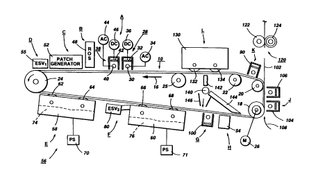
As shown in Figures 2 and 3, a highlight color printing apparatus 2 in
which the invention may be utilized comprises a xerographic processor
module 4, an electronics module 6, a paper handling module 8 and a user
interface (IC) 9. A charge retentive member in the form of an Active Matrix
(AMAT) photoreceptor belt 10 is mounted for movement in an endless path
past a charging station A, an exposure station B, a test patch generator
station C, a first Electrostatic Voltmeter (ESV) station D, a developer station
E, a second ESV station F within the developer station E, a pretransfer
station G, a toner patch reading station H where developed toner patches are
sensed, a transfer station J, a preclean station K, cleaning station L and a
fusing station M. Belt 10 moves in the direction of arrow 16 to advance
successive portions thereof sequentially through the various processing
stations disposed about the path of movement thereof. Belt 10 is entrained
about a plurality of rollers 18, 20, 22, 24 and 25, the former of which can
used as a drive roller and the latter of which can be used to provide suitable
tensioning of the photoreceptor belt 10. Motor 26 rotates roller 18 to advance
belt 10 in the direction of arrow 16. Roller 18 is coupled to motor 26 by suitable
means such as a belt drive, not shown. The photoreceptor belt may comprise a
flexible belt photoreceptor. Typical belt photoreceptors are disclosed in US-A
4,588,667 issued on 5113186, US-A 4,654,284 issued on 3131187 and US-A
4,780,385 issued on 10/25/88.
As can be seen by further reference to Figures 2 and 3, Initially
successive portions of belt 10 pass through charging station A. At charging
station A, a primary corona discharge device in the form of dicorotron
indicated generally by the reference numeral 28, charges the belt 10 to a
selectively high uniform negative potential, V0. As noted above, the initial
charge decays to a dark decay discharge voltage, Vddp~ (VCAD). The dicorotron
is a corona discharge device including a corona discharge electrode 30 and a
conductive shield 32 located adjacent the electrode. The electrode is coated
with relatively thick dielectric material. An AC voltage is applied to the
dielectrically coated electrode via power source 34 and a DC
,,~
2~ ~7~
.~,
voltage is applied to the shield 32 via a DC power supply 36. The delivery of
charge to the photoconductive surface is accomplished by means of a
displacement current or capacitative coupling through the dielectric
material. The flow of charge to the P/R 10 is regulated by means of the DC
bias applied to the dicorotron shield. In other words, the P/R will be
charged to the voltage applied to the shield 32. For further details of the
dicorotron construction and operation, reference may be had to US-A
4,086,650 granted to Davis et al on April 25, 1978.
A feedback dicorotron 38 comprising a dielectrically coated
electrode 40 and a conductive shield 42 operatively interacts with the
dicorotron 28 to form an integrated charging device (ICD). An AC power
supply 44 is operatively connected to the electrode 40 and a DC power
supply 46 is operatively connected to the conductive shield 42.
Next, the charged portions of the photoreceptor surface are
advanced through exposure station B. At exposure station B, the uniformly
charged photoreceptor or charge retentive surface 10 is exposed to a laser
based input and/or output scanning device 48 which causes the charge
retentive surface to be discharged in accordance with the output from the
scanning device. Preferably the scanning device is a three level laser Raster
Output Scanner (ROS). Alternatively, the RO5 could be replaced by a
conventional xerographic exposure device. The ROS comprises optics,
sensors, laser tube and resident control or pixel board.
The photoreceptor, which is initially charged to a voltage V0,
undergoes dark decay to a level Vddp or VCAD equal to about -900 volts to
form CAD images. When exposed at the exposure station B it is discharged
to Vc or VDAD equal to about -100 volts to form a DAD image which is near
zero or ground potential in the highlight color (i.e. color other than black)
parts of the image. See Figure la. The photoreceptor is also discharged to
Vw or Vmod equal to approximately minus 500 volts in the background
(white) areas.
A patch generator 52 (Figures 3 and 4) in the form of a
conventional exposure device utilized for such purpose is positioned at the
patch generation station C. It serves to create toner test patches in the
-20-
- 2~79~
interdocument zone which are used both in a developed and undeveloped
condition for controlling various process functions. An Infra-Red
densitometer (IRD) 54 is utilized to sense or measure the reflectance of test
patches after they have been developed.
After patch generation, the P/R is moved through a first ESV
station D where an ESV (ESV1) 55 is positioned for sensing or reading
certain electrostatic charge levels (i. e. VDAD, VCAD, VMod, and Vtc) on the
P/R prior to movement of these areas of the P/R moving through the
developmentstation E.
At development station E, a magnetic brush development
system, indicated generally by the reference numeral 56 advances
developer materials into contact with the electrostatic latent images on the
P/R. The development system 56 comprises first and second developer
housing structures 58 and 60. Preferably, each magnetic brush
development housing includes a pair of magnetic brush developer rollers.
Thus, the housing 58 contains a pair of rollers 62, 64 while the housing 60
contains a pair of magnetic brush rollers 66, 68. Each pair of rollers
advances its respective developer material into contact with the latent
image Appropriate developer biasing is accomplished via power supplies
70 and 71 elenrically connected to respective developer housings 58 and
60. A pair of toner replenishment devices 72 and 73 (Figure 2) are provided
for replacing the toner as it is depleted from the developer housing
structures 58 and 60.
Color discrimination in the development of the electrostatic
latent image is achieved by passing the photoreceptor past the two
developer housings 58 and 60 in a single pass with the magnetic brush rolls
62, 64, 66 and 68 electrically biased to voltages which are offset from the
background voltage VMod~ the direction of offset depending on the
polarity of toner in the housing. One housing e.g. 58 (for the sake of
illustration, the first) contains red conductive magnetic brush (CMB)
developer 74 having triboelectric properties (i. e. negative charge) such that
it is driven to the least highly charged areas at the potential VDAD of the
latent images by the electrostatic development field (VDAD ~ Vcolor bias)
~l~ 7~7
''~ between the photoreceptor and the development rolls 62, 64. These rolls
are biased using a chopped DC bias via power supply 70.
The triboelectric charge on conductive black magnetic brush developer
76 in the second housing is chosen so that the black toner Is urged towards
the parts of the latent images at the most highly charged potential VCAD by
the electrostatic development field (VCAD ~ Vblack bias) existing between the
photoreceptor and the development rolls 66, 68. These rolls, like the rolls
62, 64, are also biased using a chopped DC bias via power supply 71. By
chopped DC (CDC) bias is meant that the housing bias applied to the
developer housing is alternated between two potentials, one that represents
roughly the normal bias for the DAD developer, and the other that represents
a bias that is considerably more negative than the normal bias, the former
being identified as VBias Low and the latter as VBjas Hiç~h This alternation of the
bias takes place In a periodic fashion at a given frequency, with the period of
each cycle divided up between the two bias levels at a duty cycle of from 5-
10 % (Percent of cycle at VBjasHj~,h) and 9095% at VBjas,oW. In the case of the
CAD image, the amplitude of both VBjas Low and VBjas High are about the same as
for the DAD housing 58, but the waveform is inverted in the sense that the
bias on the CAD housing 60 is at VBjas Hi~h for a duty cycle of 90-95%.
Developer bias switching between VBias Hiç~h and VBjas Low~ iS effected
automatically via the power supplies 70 and 74. For further details regarding
CDC biasing, reference may be had to U. S. Patent Application Serial No.
440,913 filed November 22, 1989 in the name of Germain et al and
assigned to same assignee as the instant application.
In contrast, in conventional tri-level imaging as noted above, the CAD
and DAD developer housing biases are set at a single value which is offset
from the background voltage by approximately -100 volts. During image
development, a single developer bias voltage is continuously applied to each
of the developer structures. Expressed differently, the bias for each
developer structure has a duty cycle of 100%.
Because the composite image developed on the photoreceptor
consists of both positive and negative toner, a negative pretransfer
~,:
~7~ ~t~
,._
dicorotron member 100 at the pretransfer station G is provided to
condition the toner for effective transfer to a substrate using positive
corona discharge.
Subsequent to image development a sheet of support material
102 (Figure 3) is moved into contact with the toner image at transfer station
J. The sheet of support material is advanced to transfer station J by
conventional sheet feeding apparatus comprising a part of the paper
handling module 8. Preferably, the sheet feeding apparatus includes a feed
roll contacting the uppermost sheet of a stack copy sheets. The feed rolls
rotate so as to advance the uppermost sheet from stack into a chute which
directs the ad~lancing sheet of support material into contact with
photoconductive surface of belt 10 in a timed sequence so that the toner
powder image developed thereon contacts the advancing sheet of support
material attransferstation J.
Transfer station J includes a transfer dicorotron 104 which sprays
positive ions onto the backside of sheet 102. This attracts the negatively
charged toner powder images from the belt 10 to sheet 102. A detack
dicorotron 106 is also provided for facilitating stripping of the sheets from
the belt 10.
After transfer, the sheet continues to move, in the direction of
arrow 108, onto a conveyor (not shown) which advances the sheet to fusing
station M Fusing station M includes a fuser assembly, indicated generally
by the reference numeral 120, which permanently affixes the transferred
powder image to sheet 102. Preferably, fuser assembly 120 comprises a
heated fuser roller 122 and a backup roller 124. Sheet 102 passes between
fuser roller 122 and backup roller 124 with the toner powder image
contacting fuser roller 122. In this manner, the toner powder image is
permanently affixed to sheet 102 after it is allowed to cool. After fusing, a
chute, not shown, guides the advancing sheets 102 to a catch trays 126 and
128 (Figure 2), for subsequent removal from the printing machine by the
operator.
After the sheet of support material is separated from
photoconductive surface of belt 10, the residual toner particles carried by
the non-image areas on the photoconductive surface are removed therefrom.
These particles are rmoved at cleaning station L. A cleaning housing 130
supports therewithin two cleaning brushes 132, 134 supported for counter-
rotation with respect to the other and each supported in cleaning relationship
with photoreceptor belt 10. Each brush 132, 134 is generally cylindrical in
shape, with a long axis arranged generally parallel to photoreceptor belt 10,
and transverse to photoreceptor movement direction 16. Brushes 132,134
each have a large number of insulative fibers mounted on base, each base
respectively journaled for rotation (driving elements not shown). The brushes
are typically detoned using a flicker bar and the toner so removed is
transported with air moved by a vacuum source (not shown) through the gap
between the housing and photoreceptor belt 10, through the insulative fibers
and exhausted through a channel, not shown. A typical brush rotation speed
is 1300 rpm, and the brush/photoreceptor interference is usually about 2
mm. Brushes 132, 134 beat against flicker bars (not shown) for the release
of toner carried by the brushes and for effecting suitable tribo charging of thebrush fibers.
Subsequent to cleaning, a discharge lamp 140 floods the
photoconductive surface 10 with light to dissipate any residual negative
electrostatic charges remaining prior to the charging thereof for the
successive imaging cycles. To this end, a light pipe 142 is provided.
Another light pipe 144 serves to illuminate the backside of the P/R
downstream of the pretransfer dicorotron 100. The P/R is also subjected to
flood illumination from the lamp 140 via a light channel 146.
Figure 4 depicts the the interconnection among active components of
the xerographic process module 4 and the sensing or measuring devices
utilized to control them. As illustrated therein, ESV1, ESV2 and IRD 54 are
operatively connected to a control board 150 through an analog to digital
(A/D) converter 152. ESVI and ESV2 produce analog readings in the range of
0 to 10 volts which are converted by Analog to Digital (A/D) converter 152
to digital values in the range 0-255. Each bit corresponds to 0.040 volts
(10/255) which is equivalent to photoreceptor voltages in the range 0-1 500
where one bit equals 5.88 volts (1 500/255).
-24-
The digital value corresponding to the analog measurements are
processed in conjunction with a Non-Volatile Memory (NVM) 156 by
firmware forming a part of the control board 150. The digital values arrived
at are converted by a digital to analog (D/A) converter 158 for use in
controlling the ROS 48, dicorotrons 38, 90, 100, 104 and 106. Toner
dispensers 160 and 162 are controlled by the digital values. Target values
for use in setting and adjusting the operation of the active machine
components are stored in NVM.
When the undeveloped CAD image on the P/R passes through the
DAD developer housing structure 58, the color developer material
experiencesaverylargecleaningfield. Due to the conductivity of the color
developer material 74, electric charges will pass from the color developer
material to the photoreceptor, reducing the voltage of the black or CAD
latent image. Accordingly, a second ESV 80 (ESV2) positioned intermediate
the developer structures 58 and 60 is provided for reading or sensing VCADI
VDADI and Vtb.
The amount of CAD image voltage lost in passing through the color or
DAD developer housing is not constant. In particular, the loss Is higher as
the voltage entering the color development zone increases. Thus, as the P/R
ages and dark decay increases the voltage loss becomes worse. Now, as the
loss becomes higher the voltage at the charging station must be increased to
compensate for it. This, in turn, increases the voltage at the color housing
and a runaway situation can occur. This condition occurs when the slope of
a loss (VCAD@ESV1 VCAD@ESV2) VS incoming voltage (VCAD@ESV1 ~ VCOIOr
bias) curve exceeds 1.
If the voltage entering the color housing exceeds this "breakdown"
point, then normal control decisions (i.e. increasing the charge level of the
P/R) may no longer be proper. Any further increase in the charge voltage will
result in a lower voltage on the P/R following the color housing. For
example, if at the current voltage, the slope of the curve is 1.5 then a 10
volt increase in charge would result in a 15 volt higher loss and the voltage
after the color housing would actually go down by 5 volts, not counting dark
decay) .
-25-
2~7~ ~9~
. ,~
ESVl monitors the CAD voltage entering the color housing and
when it exceeds a critical value, further increases in the control of the
charging dicorotrons is prevented, even if the voltage at ESV2 is too low. In
this manner the life of an aged P/R is somewhat extended and catastrophic
control runaway is prevented.
Tri-level xerography requires fairly precise electrostatic control
at both development stations. This is accomplished by using ESV1 and ESV2
to measure voltage states on the P/R in test patch areas written in the
interdocument zones between successive images. However, because the
color developer material reduces the magnitude of the black development
field in a somewhat variable manner, it is necessary to read the
electrostatics associated with the black development following the color
housing.
In such a system it is necessary that the ESVs are reasonably
precise in their readings. Although the ESVs can be calibrated to a common
source by a service rep, the ESV output is known to drift over time if
charged toner particles are deposited within the unit. A single ESV cannot
distinguish between charge on the P/R and charge on a toner particle
sitting inside the ESV housing.
In the dual ESV control system such as disclosed herein, ESV1 is
taken as the reference for calibration purposes since it is less prone to
contamination. At each cycle up, following a normal cycle down, there is a
portion of the P/R that has been exposed by a multi-functional erase lamp
140 but not charged by the charging system. This portion of the P/R is at or
below the residual voltage left on the P/R and experiences very little dark
decay.
An ESV output is established to record a one volt offset when it
reads zero volts on the P/R. When converted from 0-10 volts analog to 0-
255 bits digital, each bit corresponds to 0.040 volts analog which is
equivalent to a reading of approximately 5.88 volts on the P/R surface. A
P/R voltage of 59 volts, for example will produce an ESV reading of 35 bits,
including the 25 bit offset.
-26-
2~76 lg ~
. ,.,~
At such low voltages, where P/R dark decay is small, both ESV1
and ESV2 should read the same voltage if they are properly calibrated.
Contamination by charged particles will change the reading of one or both
ESVs.
At each cycle up following a normal cycle down, the relatively
uncharged portion of the P/R is read by both ESVs as the P/R is put into
motion. Using ESV1 as a reference, the zero offset of ESV2 is adjusted to
achieve the same residual P/R voltage reading as ESV1. This new offset is
stored in Non-Volatile Memory (NVM) and is used to adjust all subsequent
ESV2 voltage readings until a new offset is measured. In this way any
contamination of the ESV2 probe by charged particles is eliminated from
the ESV1 readings.
As depicted in Figure 4, analog voltage signals representing
ESV1 and ESV2 readings are transmitted to the Analog to Digital (A/D)
converter 152. The digital values arrived at in the A/D are utilized by an
electronic control board 150 for storing the new offset mentioned above in
NVM. The stored offset is utilized in adjusting all subsequent CAD image
readings by ESV2. The electronics and logic circuitry of the control board
compares the CAD image reading by ESV2 less the new offset stored in NVM
to the stored target in NVM. The difference value of the CAD voltage level
is used via the Digital to Analog (D/A) converter 158 to adjust the DC
voltage applied to the shield 42 of the dicorotron 38. As noted above ESV1
monitors the CAD voltage and when it exceeds a target value stored in
memory it takes over control of the feedback dicorotron 38. ESV1 readings
are used to prevent changes to Vo if VCAD @ ESV1-Vcolor bias iS greater than
target. The system does not act to reduce Vo (and, thus VCAD #ESV1 if it is
too high.