Note: Descriptions are shown in the official language in which they were submitted.
-- 2û76897
BROADBAND CONFORMAL INCLINED
SLOTLINE ANTENNA ARRAY
BACKGROUND OF THE INVENTION
The present invention relates to antenna arrays, and
more particularly to conformal arrays useful for missile
applications.
U.S. Patent 5,023,623, entitled "Dual Mode Antenna
Apparatus Having Slotted Waveguide and Broadband Arrays,"
by Donald E. Kreinheder et al. provides a description of
conventional missile target detection and tracking
systems. Briefly, one type of target tracking system is
known as broadband anti-radiation homing (ARH). Such a
system is passive, and tracks a target by receiving
radiation emitted by the target.
Known conformal arrays for missiles employ conformal
slot radiators and microstrip patch radiators. These
antennas are narrow band, and because of their physical
and/or electrical characteristics they can not be inclined
to enhance their forward radiation. The result is a
limited field of view.
Conventional conformal mounting situates the antenna
elements so they face normal to the missile surface result-
ing in poor radiation in the forward direction. This is
because the antenna is situated so that the greatest amount
A 25 of energy from each element is directed normally to the
l~ ~
-
-` 207~897
missile body. This makes radiation in the forward direc-
tion difficult. The problem is made worse for elements
radiating with an E-field tangential to the metallic
missile body. The metal surface will not support these
fields and forces them to zero at the point of contact.
This is a major problem for conformal arrays since their
"view" to missile boresight is tangential from the cylin-
drical section and nearly tangential in the nose region.
It is an object of an aspect of the present invention
to provide an ARH missile guidance antenna that is
conformal to the missile surface, is dual-polarized, and
broadband.
An object of an aspect of the invention is to provide
a conformal antenna array for a missile that will sense RF
radiation over the forward hemisphere.
SU~RY OF THE INVENTION
An array in accordance with an aspect of the invention
uses broadband antenna elements with both the E and the
H-plane elements inclined toward boresight to improve
directivity in that direction. This offsets the nullifying
effects of the metallic skin in the H-plane as well as
enhances the performance of the E-plane. Tilting the
elements also makes the antenna more compact which helps in
adapting it to conformal use.
The antenna uses slotline (notch) elements which have
a flat profile. These elements are suitable for close
packing in both the E and H-planes to prevent grating lobes
in the antennas' field of view while the antenna is scanned
to boresight. Slotline (notch) elements are broadband with
greater than three-to-one bandwidths being achieved. Dual
polarization is accomplished by combining the E and H-plane
elements in a linear or circumferential manner. A single
or dual polarized array can be mounted on the cylinder
section, on the nose, or radially around the missile body.
r
2~76897
In the radial configuration, the elements still incline in
the boresight direction. Any combination of array
positions is possible. The slotline elements can be packed
with spacing close enough to allow for electronic beam
steering without creating grating lobes at the highest
frequency of operation.
Other aspects of this invention are as follows:
An array of aligned flared notch antenna elements for
a missile, characterized in that said elements are inclined
toward boresight of said missile to improve directivity in
the direction of boresight.
A passive radar array system for detecting the
location of a target in respect to a missile boresight,
comprising:
a circumferential array of flared notch antenna
elements disposed about the circumference of a missile,
said elements inclined toward boresight to improve
directivity in the direction of boresight;
a radar processor responsive to signals received from
said array to determine the target location in relation to
the missile boresight; and
means for selectively coupling the signals from
selected ones or groups of ones of said antenna elements to
said radar processor to permit the processor to determine
the particular antenna having the highest output signal and
to form a receiving sub-array comprising said particular
antenna element and a number of adjacent antenna elements.
In a missile, a passive radar array system for
detecting the location of a target, comprising:
a longitudinal array of flared notch antenna elements
disposed longitudinally along a portion of exterior surface
of said missile, said elements inclined toward boresight to
improve directivity in the direction of boresight;
~ 3a 2~76897
a radar processor responsive to signals received from
said array elements to determine the target location; and
means for electronically scanning a beam formed by
said longitudinal array to locate said target.
BRIEF DESCRIPTION OF THE DRAWING
These and other features and advantages of the present
invention will become more apparent from the following
detailed description of an exemplary embodiment thereof, as
illustrated in the accompanying drawings, in which:
FIG. 1 illustrates a conventional tapered slotline
antenna element.
FIGS. 2 and 3 are respective top and side views of an
H-plane array wherein the elements are inclined toward
boresight in accordance with the invention.
FIG. 4 illustrates a tapered notch inclined element
array of symmetrical E-plane elements.
FIG. 5 illustrates a tapered notch inclined element
array of asymmetrical E-plane elements.
FIG. 6 illustrates a linear array of inclined E-plane
elements with modified tapers to accommodate the inclina-
tion.
FIG. 7 illustrates a dual polarization antenna employ-
ing two inclined E-plane arrays flanking one inclined H-
plane array in accordance with the invention.
FIG. 8 illustrates another embodiment of a dual
polarization antenna in accordance with the invention,
employing a pair of inclined H-plane elements on each
inclined card, with the inclined elements of the E-plane
array positioned between them.
2076897
FIGS. 9-11 illustrate a circumferential array of
inclined E and H-plane elements of a conformal antenna in
a missile in accordance with the invention.
FIGS. 12-14 illustrate three exemplary arrangements of
linear inclined element arrays within a missile body in
accordance with the invention.
FIG. 15 illustrates the interconnection of the E-plane
elements of a circumferential array embodying the inven-
tion.
FIG. 16 illustrates the interconnection of the H-plane
elements of a circumferential array embodying the inven-
tion.
FIG. 17 illustrates the combining of a sub-array
comprising selected ones of the elements of an inclined
element array in accordance with the invention.
FIG. 18 is an end view of a missile illustrating the
arrangement of longitudinal arrays of inclined elements in
accordance with the invention.
FIG. 19 is a schematic diagram illustrative of a dual
polarization array system employing a longitudinal array of
inclined elements, comprising N pairs of E-plane elements
and N H-plane elements.
FIG. 20 is a schematic diagram illustrative of a dual
polarization array system employing a longitudinal array of
inclined elements, comprising N pairs of H-plane elements
and N E-plane elements.
DETAILED DESCRIPTION OF THE PREFERRED EMBODIMENT
- The invention employs the tapered slotline antenna
element sometimes referred to as a tapered notch element.
FIG. 1 illustrates an unmodified slotline 30. A compen-
sated feed 32 transitions energy to a flared dielectric
notch 34 which launches the energy to free space.
-
`- 2076897
As in the antenna of U.S. Patent 5,023,623, an array
embodying the present invention employs a plurality of
tapered notch antenna elements to comprise the antenna
array. To enhance directivity toward boresight, however,
the antenna elements are inclined in accordance with the
invention. Any inclination angle between O and 90 degrees
may be used in accordance with the invention, although 30
and 90 are preferred inclination angles. The inclination
is illustrated for a typical H-plane array in the top view
of FIG. 2 and the edge view of FIG. 3. Here a plurality of
tapered notch radiator elements 3OA, 3OB, ... 3ON are
arranged in a spaced, parallel relationship. Instead of
each radiator being set at a perpendicular with respect to
the same reference horizontal line, as in the conventional
array of tapered notch radiator elements, the respective
elements are inclined by an inclination angle ~ which is
less than 90, and typically 30 or 45. The spacing
between adjacent edges of the inclined radiator elements is
less than or equal to lh/2, where Ah is the shortest
wavelength of operation of the array. If the spacing is
greater than Ah/2, undesirable grating lobes can be formed
at the higher frequencies of operation. The desired
spacing and inclination angle of the H-plane elements is
obtained with fixturing, i.e., the rigid structural frame
which holds the antenna elements in position and fastens
the elements to the missile body.
In the E-plane, the conventional tapered slotline
elements, such as are used in the array of U.S. Patent
5,023,623, require modification in order to incline them
toward boresight. Symmetrical or asymmetrical embodiments
for the tapered regions of the slotline radiators can be
employed. The asymmetrical flared notch elements can fit
more easily into an inclined profile, and can be spaced
more compactly so the An/2 spacing rule is not broken.
However, asymmetrical elements provide a poorer match into
- -~ 207 689~
the antenna causing higher VSWR and a reduction in the
antenna's efficiency. Symmetrical flared notch elements
present a better match (lower VSWR) and therefore provide
a higher antenna efficiency. However, the symmetry limits
the inclination angle of the array toward boresight and
limits the close packing needed to maintain the An/2
spacing.
- FIG. 4 illustrates a tapered notch inclined element
array 40 of a plurality of adjacent elements formed on the
same dielectric substrate. Here the flaring on either side
of the notch is symmetrical while each element is inclined
by an angle ~ from the horizontal.
FIG. 5 illustrates an array of E-plane elements 45
which are also inclined by angle ~, but wherein the flaring
on the respective sides of the notch is asymmetrical.
FIG. 6 illustrates a linear array 50 comprising a
plurality of asymmetrical E-plane elements 52A-52N with
modified tapers to accommodate the inclination.
The antenna elements may be fabricated using conven-
tional techniques to build flared notch stripline antenna
elements. Each element is typically fabricated from a
dielectric substrate board initially clad with copper
layers on each surface. The board may comprise, for
example, fiberglass reinforced Teflon ~ The copper layer
on one surface is partially etched away to form the flared
notch; the copper surface on the opposite layer is selec-
tively etched to form the balun circuit and feed network.
Further details of the manner of construction may be found
in U.S. Patent 5,023,623.
There are at least two approaches to dual polarization
for the linear array employing inclined radiator elements
in accordance with the invention. One approach, illustrat-
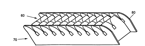
ed in FIG. 7, employs an inclined H-plane array 60 flanked
on both sides by inclined E-plane arrays 70 and 80.
Another approach, illustrated in FIG. 8, comprises an
r~
207~897
-
inclined H-plane array 90 of double slotline elements,
i.e., each inclined array element includes a pair of
tapered notch elements. An inclined E-plane array 9S is
positioned along the center line of the inclined H-plane
array 90, between the pairs of the H-plane radiator ele-
ments.
A circumferential array 100 of inclined E and H-plane
elements in accordance with the invention and mounted
within a missile body 105 is shown in FIG. 9. In this
array, as described above with respect to FIGS. 7 and 8,
the elements of both the E-plane and H-plane array are
inclined toward boresight. Element 102 is an exemplary H-
plane element; elements 104A and 106A represent an exempla-
ry E-plane element pair. FIG. 10 is an end view of the
array 100 of FIG. 9 taken from the nose end of the missile,
and illustrates the E-plane elements 104A, 104B, etc. The
circumferential array can be positioned on the cylindrical
portion 108 of the missile as shown in FIG. 9, or on the
sloped surface region (see 109 of FIG. 11) of the nose.
Keeping the ARH antennas on the cylindrical region 108
prevents their interference with other sensor combinations
in the nose.
Typically, the cylindrical portion of the missile body
is formed of a metallic, electrically conductive material,
while the nose end or radome is fabricated of a dielectric
material, e.g., from a sandwiched construction of rein-
forced Teflon skins and polyamide glass honeycomb.
FIG. 11 is a broken-away side view of a missile 128
employing a circumferential array 110 of inclined flared
notch radiating elements. In this example, the circum-
ferential array is disposed in the cylindrical portion 127
of the missile body 128. The array 110 includes N H-plane
inclined radiating elements 112, and N pairs of E-plane
radiating elements 114 and 116, the elements of a given
pair flanking a corresponding H-plane element.
- 207~897
The linear arrays in accordance with the present
invention can be positioned on the cylindrical portion, on
the aft portion of the nose, or near the front of the nose
while still leaving room within the nose for other sensors
such as IR sensors. FIGS. 12-14 illustrate three exemplary
arrangements.
FIG. 12 shows a missile 130 in side broken-away view,
with longitudinal arrays 132 and 134 of inclined flared
notch elements in accordance with the invention disposed
adjacent to and conforming to the contour of the cylindri-
cal portion of the missile body.
FIG. 13 illustrates a missile 140 wherein longitudinal
arrays 142 and 144 are disposed in the aft portion of the
missile nose and conform to the contour of the missile
body.
FIG. 14 illustrates a missile 145 wherein longitudinal
arrays 146 and 147 are disposed in the forward portion of
the missile nose and conform to the contour of the missile
body.
When the arrays in accordance with the invention are
mounted in the nose section of the missile, it is not
necessary that the entire nose section be fabricated of a
dielectric material. Rather the nose can be of a metal
skin with dielectric windows formed in the metal skin over
the antenna arrays.
OPeration of the Conformal ArraY.
Consider the circular 360 degree circumferential array
extending around the missile fuselage, as shown in FIGS. 15
and 16. The array 200 comprises both E and H plane ele-
ments, with the H-plane elements 201, 202... shown in FIG.
15. The array 200 further comprises a switch 210 that
allows selection of each H-plane element in the array and
makes it possible for the processor 212 to compare the
20768!97
-
amplitude of the target's signal at each H-plane element.
While shown as a single element, switch 210 actually
comprises a switch for each H-plane element so that more
than one element can be selected at any given time. Simi-
larly, the outputs of the pairs of E-plane elements adja-
cent each H-plane element are combined and fed to a switch
230 which allows the processor 212 to select the E-plane
element pair with the largest signal. For example, E-plane
pair 220 and 221 adjacent H-plane element 201 are combined
in combiner 222, and E-plane element 226 and 227 adjacent
H-plane element 203 are combined in combiner 228. The
signals from the respective combiners are fed into the
switch 230, and the switch output fed to the processor 212.
Here again, the switch 230 actually comprises a separate
switch for each E-plane element pair, to allow more than
one element pair to be selected at any given time.
The H-plane element or E-plane element pair with the
highest signal indicates the best position for centering a
subarray of 8, 10 or more elements for accurate target
tracking. By comparing the amplitude of the E and H plane
elements, one can determine which polarization to track
with, i.e., either the E or H plane array elements. The
outputs of the chosen elements for the array in the best
performing polarization is directed into a conventional sum
and difference network.
FIG. 17 shows a schematic diagram of an exemplary
network of selected array elements. In this example, eight
E or H plane pairs or elements are selected at positions
151-158 by either switch 210 or 230 to track the target.
The element with the highest target signal is set at
position 154 or 155 in the array. The signals from array
element positions 151-154 are fed into a 4-way combiner
160, and the signals from array element positions 155-158
are fed into a second 4-way combiner 162. The outputs of
the respective combiners are fed to a circuit 164 which
207~89q
develops the sum and difference of the respective combined
signals from combiners 160 and 162. The circuit 164 can
comprise, for example, a magic Tee or 180 degree hybrid
circuit.
Now consider an axial or longitudinal array. There
are two configurations, one having 2 H-plane elements and
one E-plane element. The other has two E-plane and one H-
plane element. Both configurations require that the pairs
be tied together to form a phase center between them.
These paired elements are treated as one element in the
array. A phase progressive phase shift is used to scan the
array.
A plurality of longitudinal arrays are typically
spaced at 45 or 90 degrees increments about the missile
fuselage. The amplitude from each longitudinal array is
sampled by the processor. The array with the strongest
signal is selected to do the tracking. Thus, in FIG. 18,
longitudinal arrays 251-258 are spaced in 45 degree incre-
ments about the missile fuselage. The signal from each
array is fed to a multiplexing switch 260 whose output is
fed to the processor.
FIG. 19 is a schematic block diagram illustrative of
an exemplary longitudinal array 280, comprising N H-plane
elements and corresponding N pairs of E-plane elements.
The E-plane element pairs 282A and 283A, 282B and 283B
282N and 283N are respectively connected to 2-way combiners
to combine the signal contributions from each E-plane pair
element; exemplary combiners 288 and 292 are shown in FIG.
19. The combiner outputs are fed to a multiplexing switch
which selects between the E-plane combiner or the corre-
sponding H-plane element. Thus, for example, H-plane
element 281A is connected to switch 286, which selects
between the H-plane element 281A and E-plane combiner 288
output. Switch 290 selects between the output of 2-way
combiner 292 and H-plane element 281B.
- 2076~97
The switch outputs are then fed to respective variable
phase shifters 294, 296 ..., and fed into one of two N/2
combiner networks 298 and 300. The elements on one side of
the longitudinal array center line 306 are fed to combiner
298, and those on the other side of the line are fed to
combiner 300. The combiner outputs are fed to a sum and
difference network 302, and the respective sum and differ-
ence signals are sent to the processor 304. The processor
304 selects the E or H plane elements to scan for the
target, and uses the phase scan angle and the sum and
difference signal data to identify the target location or
bearing.
FIG. 20 is a schematic diagram illustrating a longitu-
dinal array 320 employing N E-plane elements and 2N H-plane
elements. This embodiment is similar to that of FIG. 19,
except it is the H-plane element pairs whose outputs are
combined in a 2-way combiner, and multiplexed with the
output of the corresponding E-plane element. Thus, H-plane
elements 322A and 323A are connected to a 2-way combiner
326. Multiplexing switch 328 selects either the output of
the combiner 326 or the E-plane element 324. The selected
output is then fed to a variable phase shifter 330, and the
phase shifted output is fed into an N/2 combiner network
332. The elements on the other side of the array center
line 336 are combined in N/2 combiner 334. The respective
N/2 combiner outputs are sent to a sum and difference
circuit 338, and the sum and difference output data is sent
to the processor 340. Here again, the processor selects
the E or H plane to scan for the target, depending on the
target's polarization. The processor 340 employs the scan
angle and the sum and difference signal data to identify
the target location.
It is understood that the above-described embodiments
are merely illustrative of the possible specific embodi-
ments which may represent principles of the present inven-
2Q76897
12
tion. Other arrangements may readily be devised in accor-
dance with these principles by those skilled in the art
without departing from the scope and spirit of the inven-
tion.