Note: Descriptions are shown in the official language in which they were submitted.
WO91/17623 PCT/CA91/001~
207~57~
Line interface circuit with active tip and ring feed means.
________________________ _ __ _____________
Introd~ction
The invention is in the field of telephony and
5 more particularly relates to interface circuits for
supplying energizing current from a power source for
operation of a telephone set, via a telephone line, and for
coupling signals between the telephone line and a telephone
facility.
R^r~ro~.n~ of the Tn~nt;O~
One of the major expenses in a telephone system is
that of providing a line interface circuit for connecting
each and every telephone line at a central office switching
lS facility, or at a private branch exchange facility. In any
practical telephone system, the line interface circuits are
desirably inexpensive and essentially electrically robust.
During those times when a telephone set is in use, the
associated telephone line interface circuit provides an
20 energizing direct current for the telephone set, via tip and
ring leads of the telephone line. When the telephone set is
in use, it is usually referred to as being OFF HOOK, and
when the telephone set is not in use, it is referred to as
being ON HOOK. The line interface circuit is also required
25 to provide indication as to the telephone set being ON HOOK
or OFF HOOK.
In a central office, each telephone line is
typically routed from an outside environment toward a
switching facility via a main distributing frame (MDF).
30 The MDF iS a convenient place to provide protection from
high voltage and current transient energies, as are from
time to time conducted by one or more of the telephone lines
as the result of a utility power line cross or a lightning
strike. Protection is usually provided by the well known
35 means of gas tubes which are arranged to conduct currents
associated with potentials in excess of a thousand volts to
a heavy ground bus bar. Tip and ring leads of each
telephone line extend from the MDF to one of the line
interface circuits.
W O 91/17623 P(~r/CA91/00124
2076S76
Each line interface circuit is provided by circuit
board mounted components which includes tip and ring
terminals for connection to a telephone line and power
terminals for connection to a source for the energizing
5 current, usually a central battery supply. The central
battery supply is continually charged to a predetermined
voltage by a battery charging apparatus, provided for that
purpose. The battery charging apparatus is operated from
utility power, but in the event of an interruption of the
10 utility power the central battery supply is intended to
continue to supply operating current for a limited time.
One example of a line interface circuit is
disclosed in United States patent number 4,103,112 issued on
July 25, 1978 to v.V. Korsky, and titled ~Telephone Line
15 Circuit With Differential Loop Current Sensing And
Compensation~. A telephone line is terminated via the tip
and ring terminals by tip and ring windings of a miniature
transformer. Energizing direct current is conducted by 200
ohm tip and ring feed resistors connected in series between
20 the battery supply and the tip and ring windings. In this
example the feed resistors are used as a means for
accurately determi ni ng the amount of direct energizing
current being conducted via the transformer windings and the
telephone line so that flux compensation can prevent the
25 core of the transformer from saturating. Thus the
transformer couples communications signals while being a
barrier to substantially reduce coupling of high energy
transient signals as may result from a lightning strike or a
utility power line cross. Nevertheless secondary and
30 compensating windings of the transformer are coupled with
protection networks to further reduce exposure of
onfollowing circuitry to such transient signals. The feed
resistors are exposed to the full brunt of any transient
signals, and are therefore usually carried on a separate
35 substrate which is thermally isolated from the other line
circuit components. The feed resistors are ideally arranged
to either withstand transient signal occurrences or
decisively fail in the event of such an occurrence, so the
WO91/17623 PCT/CA9l/00124
2~7~976
maintenance of line circuit functionality will not be
plagued by marginal performance problems.
United States patents 4,484,032 and 4,514,595
issued on November 20, 1984 and April 30, 1985 to
5 S. Rosenbaum et al, teach an ~Active Impedance Transformer
Assisted Line Feed Circuit~' and ~Active Impedance Line Feed
Circuit~. One of the functions of these line interface
circuits is that of providing a required terminating
impedance via active circuit apparatus. Particularly, tip
10 and ring amplifiers are controlled in response to direct
loop current and alternating differential current signals
detected across tip and ring feed resistors, to generate the
terminating impedance and to inject alternating current
signals for transmission via the telephone line to the
15 telephone set. In the second example, the expense of a
transformer is eliminated. In the first example, a function
of the transformer is not intended to include a reduction of
transient energies. In both examples, this function is
typically provided by a pair of diodes connected between the
20 power terminals and each of the tip and ring terminals so
that any transient energies traversing the tip and ring
leads from the MDF are diverted to the power terminals.
As the line currents detected are used as
indication of alternating current signals in the telephone
25 line and indication of direct energizing current, the
performance of the line interface circuit is contingent upon
the values of the feed resistors being very closely matched.
The operating characteristics are co~ rol"ised in proportion
to the tip and ring feed resistors becoming mismatched.
30 Such mismatch may occur during the normal use of a line
interface circuit, as one of the tip and ring feed resistors
may age in response to unusual stress, as may be caused by
transient electrical events such as a power line cross or a
lightning strike, in association with the telephone line, in
35 spite of the diode protection at the tip and ring terminals.
In some instances other circuits in the typical
electronic telephone switching office have been found to be
at risk of failure particularly in the event of a wide
spread transient electrical event. A nearby lightning
2076976
strike upon a telephone cable, may simultaneously affect a
multitude of telephone lines terminated in the switching
office. In such an instance, a corresponding multitude of
diode networks each couples a spike of current via the power
terminals. These simultaneous current spikes are additive
along a main power bus in the switching system and may cause
a damaging transient variation of voltages on power and
ground buses in parts of the switching facility.
It is one object of the invention to provide a
line interface circuit with tip and ring feed paths which
maintain preferred operating resistances in spite of
transient electrical events which could be expected to
adversely affect the normal operating performance of the
line interface circuit.
It is also an object of the invention to provide
line interface circuits which are electrically robust and
provide substantial isolation of power and ground buses from
transient electrical events in a telephone system.
S~m~rY of the Invention
In an operating telephone system, a line interface
is used for coupling alternating current signals, between a
telephone facility and a telephone apparatus, connected via
tip and ring leads of a telephone line. The telephone line
and the telephone apparatus are energized by direct current
supplied from a power source via tip and ring terminals
being connected to the tip and ring leads. In the line
interface, a method for supplying the direct current
comprises the steps of: valving a current flow in one
direction between the power source and the tip terminal with
a resistance of a preferred value, and substantially
shutting OFF the current flow, in response to an occurrence
of an excess voltage at the tip terminal; and valving a
current flow in an opposite direction between the power
source and the ring terminal with a resistance of a
preferred value, and substantially shutting OFF the current
s 2~76g7~
flow, in response to an occurrence of the excess voltage at
the ring terminal.
A line interface circuit, for supplying energizing
direct current from a power source via tip and ring leads of
a two wire communica~ions line connected with a telephone
apparatus, and for coupling alternating current signals
between the telephone line and an associated telephone
facility, includes tip and ring terminals for connection to
the tip and ring leads and power terminals for connection to
the power source. A coupling means is connected in series
with the tip and ring terminals for providing paths for the
energizing direct current and for the alternating current
signals. An active tip feed means is connected in series
between the tip terminal and the coupling means, and an
active ring feed means is connected in series between the
ring terminal and the coupling means. The active tip feed
means and the active ring feed means each includes: a line
terminal for connection at a respective one of the tip and
ring terminals, and an interface terminal for connection to
the coupling means; passive and active resistance elements
being connected in series between the line and interface
terminals, the passive resistance element being of a
resistance value corresponding to a predetermined fraction
of the predetermined resistance; a reference voltage divider
connected between the line and interface terminals and
defining a reference voltage tap; and valving control means
being responsive to a reference voltage at the reference
voltage tap for adjusting the resistance of the active
resistance element to a value which in summation with the
resistance of the passive resistance element provides the
predetermined resistance, and being responsive to an
occurrence of an excess of voltage at the reference voltage
tap, for adjusting the resistance of the active resistance
element toward infinity, whereby current flow via the active
feed means is substantially shut OFF.
5a 2076976
Brief Descri~tion of the Drawin~s
An example embodiment of a line interface circuit
is discussed with reference to the accompanying drawings in
which:
Figure 1 is a block schematic diagram of a typical
prior art line interface circuit which includes a diode
protection network for routing currents associated with
transient electrical events toward power and ground
conductors, for purposes of protecting onfollowing circuits,
such as signal coupling and supervision circuits and hybrid~
.
,. a. _~
`~'0 91/17623 PCT/CA91/00l24
~ _ 6 2076976
and codec circuits, from unusual potentials and currents,
which might otherwise cause damage to such circuits;
Figure 2 is a block schematic diagram of a typical
telephone central office wherein line interface circuits are
5 used to complete communications paths between telephone
lines and a telephone switching network; and
Figure 3 is a schematic diagram of an active
resistance line feed apparatus in accordance with the
invention, for use in providing tip and ring feed resistor
10 elements in a line interface circuit suitable for use in
Figure 2, and preferable without a diode protection network
of the type or similar to the diode protection network
illustrated in Figure 1.
15 De~cr;Dt~o~ of the Preferred Rmhn~ment
A brief review of the prior art, as exemplified in
Figure 1 and as used in Figure 2 is of benefit to an
understanding of the essence and application of the
invention. The prior art line interface circuit of Figure 1
20 is of a general type disclosed in the previously mentioned
patents to Rosenbaum et al. That is to say that tip and
ring terminals are connected by tip and ring feed resistors
112 and 113 to a coupling and supervision circuit. The tip
and ring terminals are driven by tip and ring amplifier
25 circuits 120 and 140 which are responsive in operation to
signals and biases from a network 165. When a telephone in
an OFF HOOK condition is connected via a telephone line to
tip and ring terminals 2 and 3, alternating current signals
and direct energizing current are detected as voltages
30 developed across tip and ring feed resistors 112 and 113.
These voltages are coupled via voltage dividers 114 to an
amplifier circuit 160 which drives into the network 165.
The network 165 transmits signals to an electronic hybrid
circuit indicated, and receives signals destined for the
35 telephone, from the electronic hybrid circuit. Neither the
electronic hybrid circuit and a codec circuit, both
indicated at 180, is shown in detail as both are well known.
The hybrid and codec circuits cooperate in providing two
wire, four wire, and analog and digital signal conversions
WO 9l/l7623 PCI/CA91/00l24
7 2076976
in a well known manner, to provide communications via a
telephone facility. The network 165 usually includes an
impedance network, not shown, which determines effective
output impedances of the tip and ring amplifiers 120 and
5 140, so that in combination with the values of the tip and
ring feed resistors 112 and 113, a prescribed telephone line
terminating impedance is in effect across the tip and ring
terminals. Satisfactory operation of the line interface
circuit relies upon the tip and ring feed resistors 112 and
10 113 being of closely matched resistance values, and for this
reason the feed resistors are usually manufactured on an
electrically insulating thermally conductive substrate and
are individually trimmed to within 0.1% of a preferred
resistance.
One of the problems with line interface circuits
which use active components is that a transient electrical
energy appearing at either of the tip or ring terminals can
be of a destructive effect. If the transient electrical
energy is of an extremely excessive, albeit momentary
20 potential, as typically results from a lightning strike upon
the telephone line, various of the amplifiers may be
destroyed. If the transient electrical energy is more in
the nature of a prolonged excessive current, as is typical
of an accidental power line cross, it may be that one or
25 both of the tip and ring feed resistors is sufficiently
stressed to become mismatched. A diode protection network
as illustrated at 100 provides the standard solution for
these problems, particularly when combined with other
protective apparatus as exemplified in Figure 2. Line
30 interface circuits 203a-n are installed in the central
office in Figure 2, between a main distributing frame (MDF)
201 and a telephone switching network 204. The MDF
terminates each telephone line connected at the central
office and provides a high voltage path for any transient
35 electrical energy traversing the telephone line. Each path
is typically provided by an individual gas tube device
indicated at 202a-n, and which is connected to each lead of
every telephone line 205a-205n. The gas tubes used for this
purpose usually become very conductive when exposed to a
WO91/17623 PCT/CA9l/00l24
8 2076976
potential difference from ground in excess of a thousand
volts. Thus transient potentials in excess of a thousand
volts are rarely ever transmitted to the tip terminal or to
the ring terminal of a line interface circuit. However, it
5 has been found that a lightning strike which spreads energy
over a multitude of telephone lines may cause overvoltage
stress leading to failures of circuits not directly
connected to affected telephone line interface circuits, but
merely connected to a power bus 206 or a ground bus 207
10 common to many of the affected line interface circuits. The
apparent cause of this effect is an additive effect of a
multitude of simultaneously conducting diode protection
networks. In spite of very low impedance characterisitics
of a central battery supply 208 to which the power and
15 ground buses 206 and 207 are connected, the simultaneously
conduction causes a momentary excursion of voltage on either
of the power and ground buses which exposes many circuits in
the telephone switching network to stresses for which they
were not designed.
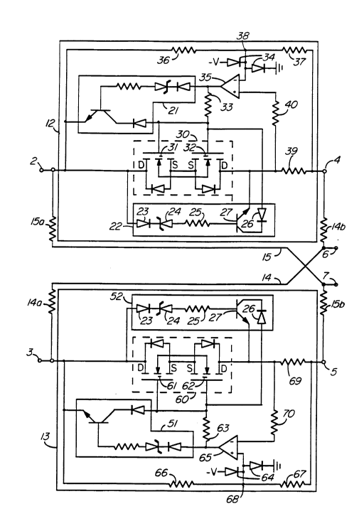
The embodiment of the invention illustrated in
Figure 3 replaces the feed resistors 112 and 113 of the line
circuit in Figure 1, with tip and ring active feed resistors
12 and 13. In order to realize all the benefits of the
invention in a telephone facility, as for example
25 illustrated in Figure 2, it is preferable that any
protection network, of function similar to the function of
the protection network 100, not be provided.
Referring to Figure 3, the active tip feed
resistance 12 is connected in series between a tip terminal
30 2, which is also referred to as a line terminal, and
coupling means, not shown, via an interface terminal 4, to
provide a path of predetermined resistance for alternating
current signals and for direct current. In the active tip
feed resistance 12, a tip reference voltage divider is
35 provided by resistors 36 and 37 connected in series between
the line terminal 2 and the interface terminal 4, and which
define a tip reference voltage tap 38. A first field effect
transistor (FET) 31 with first source, drain and gate
electrodes, and a second FET 32 with second source, drain
WO91/17623 PCT/CA9l/001~
and gate ele'ctr~des,~are connected in series such t~a~t7~ ~7 6
source electrode of one is connected to a source electrode
of the other, as shown, to provide a variable valving
circuit 30. A tip passive resistance element 39 is
5 connected in series between the second source electrode and
is of a resistance corresponding to a predetermined fraction
of the predetermined resistance. The FETS 31 and 32, and
the resistance element 39 carry virtually all of the
alternating and direct currents between terminals 2 and 4.
10 Series conductance of the FETS 31 and 32 is controlled by a
tip valving control circuit which includes a differential
amplifier circuit 35 having an inverting input connected to
the tip reference voltage tap 38, a non-inverting input
connected via a resistor 40 to the junction of the
15 resistance element 39 and the second drain electrode, and an
output being resistively connected via a resistor 33 to the
first and second gate electrodes. The differential
amplifier circuit 35 is operative to control the
conductances of the first and second FETS 31 and 32 such
20 that the active tip feed resistance 12 conducts with a
resistance corresponding to the predetermined resistance
under normal OFF HOOK operating conditions. The inverting
input of the differential amplifier circuit 35 is protected
by diodes 34 which are somewhat isolated from the tip
25 terminal 2 by the resistor 36 and hence never conduct
disturbing currents to the power bus. The active tip feed
resistance 12 also includes a tip threshold circuit which is
operative in the event of an excess of voltage appearing at
the tip terminal 2 to override the control of the
30 differential amplifier circuit 35, to switch the variable
valving circuit 30 to a very high resistance state. The tip
threshold circuit includes first and second legs 21 and 22,
each of which is provided by similar components which are
similarly labelled in the leg 22 as diodes 23 and 26, a
35 Zener diode 24, a resistor 25, and an NPN transistor 27,
being connected as illustrated. The leg 21 is responsive to
excessive voltages of positive polarity with respect to
ground, and the leg 22 is responsive to excessive voltages
W~91/17623 PCT/CA91/00124
2076976
of negative polarity with respect to a potential at the
output of the differential amplifier circuit 35.
The active ring feed resistance 13 is connected
in series between a ring terminal 3, which is also referred
5 to as a line terminal, and the previously mentioned coupling
means, via an interface terminal 5, to provide a path of
predetermined resistance for alternating current signals and
for direct current. In the active ring feed resistance 13,
a ring reference voltage divider is provided by resistors 66
10 and 67 connected in series between the line terminal 3 and
the interface terminal 5, and which define a ring reference
voltage tap 68. A third FET 61 with third source, drain and
gate electrodes, and a fourth FET 62 with fourth source,
drain and gate electrodes, are connected in series such that
15 a source electrode of one is connected to a source electrode
of the other, as shown, to provide a variable valving
circuit 60. A ring passive resistance element 69 is
connected in series between the fourth source electrode, and
is of a resistance preferably close to the resistance value
20 of the tip passive resistance element 39. The FETS 61 and
62, and the resistance element 69 carry virtually all of the
alternating and direct currents between the terminals 3 and
5. Series conductance of the FETS 61 and 62 is controlled
by a ring valving control circuit which includes a
25 differential amplifier circuit 65 having an non-inverting
input connected to the tip reference voltage tap 68, an
inverting input connected to the junction of the resistance
element 69 via a resistor 70 and the fourth drain electrode,
and an output being resistively connected via a resistor 63
30 to the third and fourth gate electrodes. The differential
amplifier circuit 65 is operative to control the
conductances of the third and fourth FETs 61 and 62 such
that the active ring feed resistance 13 conducts with a
resistance corresponding to the predetermined resistance
35 under normal OFF HOOK operating conditions. The non-
inverting input of the differential amplifier circuit 65 is
protected by diodes 64, which are somewhat isolated from the
ring terminal 3 by the resistor 66 and hence never conduct
disturbing currents to the power bus. The active ring feed
WO91/17623 PCT/CA91/00124
11 20763~6
resistance 13 also includes a ring threshold circuit which
is operative in the event of an excess of voltage appearing
at the ring terminal 3 to override the control of the
differential amplifier circuit 65, to switch the variable
5 valving circuit 60 to a very high resistance state. The
ring threshold circuit includes legs 51 and 52 which
correspond in structure and operation to the previously
mentioned legs 21 and 22 and are not further discussed.
Tip and ring voltage dividers 14 and 15 are
10 provided by resistors 14a, 14b and 15a, 15b connected as
shown across the active tip and ring feed resistors 12 and
13 to provide tip and ring voltage taps at terminals 6 and
7, which are normally connected across an input of the
amplifier 160 in Figure 1.
In this example, the value of the predetermined
resistance of each of the tip and ring active resistance
elements is 100 ohms, and the values of the passive
resistance~élements 39 and 69 are within 1% of 50 ohms.
Suitable FETs 31, 32, 61 and 62 are N channel 1000 volt
20 breakdown devices with a standard industry code 3N100. One
source of these FETs is Motorola Inc. at Schlumberger, Ill.
However it is envisioned that in quantity production a
custom integrated device will provide both the variable
valving circuits 30 and 60. The diodes 24 may be provided
25 for by 80 volt Zener diodes or by any convenient structure
with somewhat equivalent operating characteristics. All of
the remaining resistors shown may of similar values of 100
kilohms, however the resistors defining the tip and ring
voltage taps should be closely matched.