Note: Descriptions are shown in the official language in which they were submitted.
f ~~ .~. f~
PATENT
390100-2610
APPARATUS FOR PROCESSING A VIDEO STGNAL
1 BACKGROUND OF THE INVENT'rnu
2 This invention relates to apparatus for processing a
3 video signal, such as may be produced by a video camera or
4 recorded/reproduced by a video tape recorder, and, more
particularly, to such apparatus that controls various types of
6 processing operations so as to impart optimum parameters and
7 characteristics to the processed video signal.
Video signal processing of video~signals generated or
9 used by video equipment, such as a video camera or a video tape
recorder, is.well known. Typical types of such signal processing
11 include gamma correction, contour correction, AGC control, black
12 level adjustment, white balance adjustment, hue adjustment, color
13 temperature adjustment, and the like.
14 Heretofore, when such video equipment, fo2~ example, a
video camera, is preset for proper corrections and adjustments,
16 the various correction and adjustment control parameters (e.g. a
17 gamma correction control signal, an AGC control signal, a black
18 level adjustment signal, etc.) are set before the video equipment
19 is shipped for distribution, use or sale. The adjustment control
parameters are determined as functions of different
21 characteristics of the video signal produced by the video
s
22 ePParatus (e.g. the video signal produced by a video camera) and
23 ire established by an ancillary, add-on device that must be
24 connected to the video equipment. Although the adjustment
-1-
~~ ?b s V s. .4
PATENT
_ 390100-2610
1 control parameters are determined externally of the. video
2 equipment, such parameters are supplied to the video processing
3 circuits included in the video equipment whereat such parameters
4 are used to effect proper gamma correction', contour correction,
AGC control, and the like.
6 An example of how such ancillary parameter-calculating
7 apparatus is used with video equipment, such as a video camera,
is illustrated in FIG. 5. For convenience, the video camera is
9 assumed to include a CCD image sensor 90 as the image pickup
unit, but it is known that other conventional image pickup
11 devices may be used. The image signal produced by pickup unit 90
12 is supplied to and processed by a video signal processor 91,
13 which executes gamma correction, contour correction, white
. 14 balance adjustment, hue adjustment, and various other video
control and adjustment operations. As a result, the video signal
16 processor produces a luminance signal Y and a chroma signal C,
17 both properly corrected and adjusted.
i8 The operating levels or parameters for gamma
19 correction, contour correction, white balance adjustment, hue
adjustment, etc. of video signal processor 91 are derived from
21 control data stored in a programmable read only memory 92, such
22 as an EEPFtOM, or other neon-volatile memory. Such stored control
23 data are read out from the memory by a system controller 93,
24 converted to analog form by a digital-to-analog (D/A~ converter
94 and supplied to the individual processing circuits included in
-2-
PATENT
390100-2610
1 video signal processor 91. Thus,~depending upon the values of
2 the control data stored in EEPROM 92, the corresponding
3 corrections and adjustments in the video signal produced by
4 pickup unit 9o are made by video signal processor 91.
To generate the proper control data to be stored in
6 EEPROM 92, the luminance and chrominance signals Y and C produced
'1 by the video camera are analyzed. Such analysis is made by an
8 external adjustment apparatus 100 which, as shown in FIG. 5, is
9 electrically connected to the video camera. The adjustment
ZO apparatus includes a microprocessor 103 that is suitably
11 programmed to calculate the individual control and adjustment
12 parameters to obtain optimum gamma correction, contour
13 correction, white balance adjustment, hue adjustment, etc. This
14 is achieved by digitizing the luminance and chrominance signals
produced by the video camera and detecting the digitized video
15 signals by a wave detector 102. In this regard, an analog-to-
17 digital (A/D) converter 101 is selectively coupled by way of a
18 switch to receive either the luminance signal Y or the chrome
19 signal C and to digitize the luminance and chrome signals
supplied thereto. Wave detector 102 is coupled to A/D converter
21 101,and, detects level information and phase information of the
22 digitized luminance signal Y and the digitized chrome signal C.
23 ~ It is this detected level and phase information that is supplied
2~ to microprocessor 103 and used thereby to calculate the different
control parameters needed to effect optimum gamma correction,
_g-
~~~~'~
PATENT
390100-2610
1 contour correction, white balance adjustment, hue adjustment,
2 etc. For example, if the detected level and phase information
3 differ from predetermined reference levels, the microprocessor
~4 calculates those control parameters which, when supplied to video
signal processor 91, result in corrections and adjustments to the
6 video signal such that the level and phase information that is
7 detected by wave detector 102 is substantially equal to such
8 predetermined reference levels. It is seen that the calculated
control parameters are supplied from microprocessor 103 of
adjustment apparatus 100 to D/A converter 94 included in the
11 video camera, whereat such control parameters are converted to
12 analog form and used by video signal processor 91 for gamma
13 correction, contour correction, etc. The closed loop formed of
14 the video signal processor, A/D converter 101, wave detector 102,
microprocessor 103 and D/A converter 94 operates such that
16 optimum control parameters are generated by the microprocessor;
17 and these control parameters are written into memory 92 by system
18 controller 93. Thereafter, adjustment apparatus 100 may be
19 disconnected from the video camera; but the control parameters
stored in memory 92 nevertheless control video signal processor
21 91 to carry out optimum control and adjustment operations on the
22 video signal derived from pickup unit 90.
23 It is apparent that the prior art arrangement shown in
24 FIB. 5 does not permit a resetting or readjustment ef the control
parameters stored in memory 92 once adjustment apparatus 100 is
_4_
~~.j~~A~~~.,:j
PATENT
390100-2610
1 disconnected from the video camera. Thus, modifications or
2 resetting of such contral parameters, which may be needed over a
3 period of time, are not easily attainable without reconnecting
4 adjustment apparatus 100. Such adjustment apparatus often is
quite expensive and is constructed as a rather large piece of
6 equipment, thus making it expensive and inconvenient to sell such
7 adjustment apparatus along with the video camera with which it
8 may be used. Alternatively, if the adjustment apparatus normally
9 ~~is furnished qnly to skilled technicians, it may be difficult,
bothersome and expensive far the user of the video camera to seek
11 the assistance of such technicians for occasional resetting of
12 the control parameters. Thus, the quality of the video signal
13 produced by the video camera may deteriorate because adjustments
14 to the control parameters used by the video signal processor are
not made.
16 The foregoing difficulties are equally applicable to
17 other video equipment, such as video tape recorders, that include
18 video signal processors which are supplied with control
19 parameters that may require adjustment from time to time.
OBJECTS OF THE- TNVENTTON
21 . Therefore, it is an object of the present invention to
22 provide apparatus for generating video signal adjustment data to
23 ~ correct or adjust videa data, which apparatus is self-contained
24 ~rathin video equipment, such as a video camera, a record/playback
device, or the like.
_5_
/r
PATENT
390100-2610
1 Another object of this invention is to provide
2 apparatus that is easily usable by a user of video equipment so
3 as to produce adjustment control parameters for video signal
4 processing circuits and thereby effect automatic corrections and.
adjustments in a video signal.
6 A further object of this invention is to provide
7 digital video signal processing circuitry that is self-adjustable
8 to produce a video signal exhibiting optimum parameters.
An additional object of this invention is to provide
digital video signal processing circuitry which is automatically
11 adjustable to produce gamma correction, contour correction, white -
12 balance adjustment, hue adjustment, and the like, of a video
13 signal.
14 Various other objects, advantages and features of the
present invention will become readily apparent from the ensuing
16 detailed description, and the novel features will be particularly
17 pointed out in the appended claims.
18 SUM~dARY OF THE INVENTION
19 In accordance with this invention, apparatus is
provided for generating video signal adjustment data for use by
21 video signal processing circuits ~f the type that are included in
22 video equipment, such as video cameras, video record/playback
23 ~ devices, and the like. This apparatus is self-contained with the
24 video equipment and includes luminance and chroma digital signal
processors supplied with luminance and chroma adjustment control
_6_
~.~r~. ~..
,, , ~ ~ ;s. e,3''r
PATENT
390100-2610
1 data, respectively, for subjecting an input video signal, such as
2 may be produced by the video camera, to predetermined, respec-
3 Live, luminance and chrome adjustment operations so as to produce
4 adjusted digital luminance and chrome signals. A sampling
circuit operable at preselected times samples at least one of the
6 adjusted digital signals, and an adjustment control data
7 generator is responsive to the sampled digital signals for
8 generating luminance and/or chrome adjustment control data that
9 is/are supplied to the luminance and/or chrome digital signal
l0 processors.
11 In one embodiment, the input video signal is supplied
12 to the luminance and chrome digital signal processors by an
13 amplitude adjuster, such as an ACC circuit, whose gain control
14 signal is produced by the adjustment control data generator and
is supplied to a register coupled thereto for establishing such
16 amplitude adjustments. In another embodiment, the input video
17 signal is supplied to the luminance and chrome digital signal
18 processors by a DC level adjuster, such as a black level
19 adjuster, whose operation is controlled by level adjustment
control data generated by the adjustment control data generator
21 and stared in a register coupled thereto.
22 In yet another embodiment, the chrome digital signal
23 processor includes a white balance adjuster that is supplied with
24 weighting control data produced by the adjustment control data
-7-
PATENT
390100-2610
1 generator as a function of the adjusted digital chroma signal
2 that is sampled.
3 In a further embodiment, the chroina digital signal
4 processor includes a hue adjuster that is controlled by hue
weighting control data produced by the adjustment control data
6 generator in response to the adjusted digital chroma signal that
7 is sampled.
As a feature of this invention, closed loops are formed
9 by the luminance digital signal processor,~the sampler and the
adjustment control data generator and by the chroma digital
11 signal processor, the sampler and the adjustment control data
12 generator, whereby the adjustment control data that is produced
13 is fed back to the luminance and chroma digital signal processors
14 and is modified automatically, for example, with each cycle,
until the processed digital luminance and chroma signals exhibit
16 optimum characteristics.
17 BRIEF nESCRIPTI4N OF THE DRA~7INGS
18 The following detailed description, given by way of
19 example and not intended to limit the present invention solely
thereto, will best be understood in conjunction with the
21 accompanying drawings in which:
22 FIG. 1 is a b7.ock diagram of one embodiment of video
a
23 signal processing apparatus in accordance with the present
24 invention;
_g_
G,
PATENT
390100-213.0
1 FIG. 2 is a block diagram of another embodiment of the
2 present invention;
3 FIG. 3 is a flow chart representing the manner in which
4 adjustment operations are carried out by the system controller
used with the present invention;
6 FIG. 4 is a flow chart representing, as an example, the
7 hue adjustment rautine carried out by the present invention; and
FIG. 5 is a block diagram of a video camera connected
9 to an external adjustment parameter generator, for purposes of
comparison with the present invention.
11 DETAIDED DESCRIPTION OF CERTAIN PREFERRED EMBODIMENTS
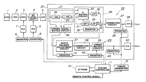
12 Referring now to FIG. 1, there is illustrated, in block
13 diagram form, one embodiment of the present invention which is
14 shown in the enwiranment of a color video camera such as a so-
called single-plate camera which uses a CCD image sensor 1 as the
16 image pickup device. Here, the CCD image sensor is provided with
17 a supplementary color coating film and produces an image output
18 signal of complementary color components read out from each of
19 the CCD elements in succession by a sample-and-hold circuit 2.
Tt is appreciated that this CCD image sensor and sample-and-hold
21 circuit are conventional and form no part of the present
22 invention per se. It will also be appreciated that other image
,,
23 pickup devices may be used from which luminance and chrome output
24 signals YoUT and CouT are derived by digital signal processor 20
which is supplied with the image signal.
PATENT
390100-2610
1 In FIG. 1, which will be described in greater detail
2 below, an input secaion is coupled to derive an input video
3 signal from the ima,e signal produced by the image pickup unit of
4 the video camera. As an example,~this input section is comprised
of an automatic gain control (AGC) circuit 3, a DC level shift
6 circuit 4 and an analog-to-digital (A/D) converter 5. AGC
7 circuit 3 is adapted to control the amplitude of the output
8 luminance signal Yom produced by digital signal processor 20.
9 Accordingly, the AGC circuit serves to amplify the image signal
l0 produced by the image pickup device in accordance with a gain
11 control signal supplied to the AGC circuit from a register 6 in
12 which the gain control signal is stored. In the preferred
13 embodiment, this stored gain control signal is in digital form,
14 and a digital-to-analog (D/A) converter 7 is coupled to register
f5 6 to convert the digital gain control signal to analog form and
16 supply that analog gain control signal to AGC circuit 3. As will
17 be described, this digital gain control signal is stored in a
19 non-volatile memory 10, such as, but not limited to, an
19 electronically erasable programmable read only memory (EEPROM).
20 The manner in which this gain control signal is produced and
21 stored in the EEPROM will be described below.
22 DC level shift circuit 4 is coupled to AGC circuit 3
23 ~ and is adapted to adjust the DC level of the output luminance
24 signal YovT eventually produced by digital signal processor 20.
25 More particularly, the DC level shift circuit operates to control
-10-
PATENT
390100-2610
1 the black level of the luminance signal to be equal to a
2 predetermined, reference black level. The amount of DC level
3 adjustment to be made to the output luminance signal is
4 determined by a black level control signal that is supplied to DC
level shift circuit 4 from a register 8. This black level
6 control signal is another of the digital adjustment and
7 correction control signals stored in EEPROM 10. Since the black
8 level control signal stored in register 8 is in digital form, and
9 since DC level shift circuit 4 is an analog circuit (in the
embodiment described herein), a D/A converter 9 is coupled to
11 register 8 to convert the digital signal to analog farm and
12 supply the analog black level control signal to the DC level
13 shift circuit.
14 The video signal whose amplitude and DC level have been
adjusted by AGC circuit 3 and DC level shift circuit 4 is
16 supplied to digital signal processor 20 by A/D converter 5. This
17 A/D converter samples the input video signal at a sampling rate
18 sufficient to produce individual pixels, and each pixel is
19 represented by a 10-bit digital signal. These digitized pixels
are coupled to digital signal processor 20 which, in the
21 preferred embodiment, is fabricated on a single IC chip.
22 Digital signal processor 20 is comprised of a delay
23 circuit 21, a luminance digital signal processor 22 and a chroma
24 digital signal processor 23. Delay circuit 21 is comprised of
cascaded delay circuits 24 and 25, each adapted to impart a delay
-11-
f;
PATENT
390100-2610
1 equal to the time period of one horizontal scan line (or 1H) to
2 the digitized pixels successively supplied thereto by A/D
3 converter 5. Thus, delay circuits 24 and 25 are referred to as
4 igi delay circuits. The output of A/D converter 5, the output of
1H delay circuit 24 and the output of 1H delay circuit 25 are
6 supplied to luminance digital signal processor 22 and also to
7 chroma digital signal processor 23. Thus, each of these digital
8 signal processors is supplied with digitized pixels exhibiting OH
9 delay, IH defy and 2H delay.
Luminance digital signal processor 22 includes a
11 luminance data generator 26 to which the OH, 1H and 2H delayed
12 pixels are supplied. The luminance data generator includes a
13 matrix circuit 30 adapted to generate luminance data YL
14 representing luminance information in a r~:latively lower
frequency band, a low pass filter 32 coupled to the output of
16 matrix circuit 30, a high pass filter 31 coupled to receive the
17 1H delayed pixel data from delay circuit 21, a low pass filter 33
18 coupled to high pass filter 31 and an adder 34 coupled to the
19 outputs of low pass filters 32 and 33. Matrix circuit 30 is
supplied with the OH, 1H and 2H delayed pixels from delay circuit
21 21 from which the low frequency band luminance data YL is
22 produced. This luminance data Y~, is supplied to adder 34 by low
i
23 pass filter 32. Tt will be appreciated that the matrix circuit
24 c~mbines the OH, 1H and 2H delayed pixels in a particular ratio
so as to produce the low band luminance data YL. This ratio is
-12-
~~~~~~J .
PATENT
390100-2610
1 determined by control data stored in a register 35 and supplied
2 therefrom to matrix circuit 30. Such combining ratio may be
3 adjusted to provide corrections for color temperature, and the
4 combining ratio. control data stored in register 35 may be thought
of as color temperature control data. Thus, as this color
6 temperature control data is adjusted (as will be described), the
7 combining ratio of the OH, 1H and 2H delayed pixels likewise is
8 adjusted to correct the low band luminance data YL for variations
in color temperature.
High pass filter 31 is coupled to the output of 1H
11 delay circuit 24 to extract data YH in a relatively higher
12 frequency band. Low pass filter 33 minimizes higher frequency
13 noise and supplies the extracted high band luminance data YH to
14 adder 34 whereat it is combined with low band luminance data YL.
The resulting luminance data produced by adder 34 is coupled to a
16 gamma correction circuit 27 from which the gamma-corrected
17 luminance data is converted to analog form by a D/A converter 28
18 and supplied as an output luminance signal YoUT to further
i9 apparatus (not shown). The output of gamma correction circuit 27
also is coupled to a register 29 which is supplied with timing
21 signals by a timing generator 12 so as to sample the luminance
22 data processed by luminance digital signal processor 22 at
23 preselected times. Depending upon such sampling times, different
24 characteristics and parameters of the processed luminance data
are sampled, such as the black level, a white level, etc. Timing
-13-
PATENT
390100-2610
1 generator 12 is controlled by system controller ll,~as will. be
2 described.
3 Chroma digital signal processor 2~3 includes a chroma
4 signal matrix circuit 36 coupled to delay circuit 21 to combine
the OH, 1H and 2H delayed pixels to produce chroma data. Matrix
6 circuit 36 is conventional and further description thereof is not
7 provided herein. The output of the chroma signal matrix circuit
B is coupled to a white balance adjustment circuit 37 which
9 operates to adjust the individual chroma components supplied
thereto by matrix circuit 36 by multiplying same with weighting
11 coefficients stored in a register 41. Such white balance
12 weighting coefficients are adjustable, as will be described, and
13 are supplied to register 41 from memory 10 in which white balance
14 weighting control data as well as other adjustment and correction
control data are stored.
16 \ The white balance adjusted chroma data produced by
17 white balance adjustment circuit 37 are supplied to a gamma
18 correction circuit 38, which may be conventional, and the gamma-
19 corrected chroma data are coupled to a linear matrix circuit 39
for hue adjustment. The linear matrix circuit is adapted to
21 adjust the chroma components supplied theret~ by multiplying same
22 s with hue adjustment weighting coefficients coupled thereto from a
23 register 42. Such weighting coefficients are referred to as hue
24 adjustment control data, and this control data is applied to
register 42 from memory 10.
14 ~°
PATENT
390100-2610
1 The chrome data output of linear matrix circuit 39 has
2 been white balance adjusted, gamma corrected and hue adjusted,
3 and this chrome data is sampled at preselected times by a
4 sampling register 43. This register is supplied with suitable
timing pulses by timing generator 12 under the control of system
6 controller 11. Such timing pulses determine the sampling times
7 of the digitally processed chrome data which, in turn, samples
8 particular characteristics and parameters of the chrome
9 information, such as white balance, hue, etc.
The digitally processed chrome data produced by linear
11 matrix circuit 39 is converted to analog form by a D/A converter
12 40 to supply a chrome output signal CouT for use by other
13 apparatus (not shown).
14 Memory 10, which may be an EEPROM, as aforementioned,
is bidirectionally coupled to system controller 1l which writes
16 correction and adjustment control data (referred to hereafter for
17 simplicity simply as adjustment control data) thereinto and reads
18 such adjustment control data to registers 6, 8, 35, 41 and 42.
19 The system controller preferably is comprised of a suitably
programmed microprocessor which generates adjustment control data
21 in response to the sampled luminance and chrome data obtained by
22 registers 29 and 43, respectively. Changes in the adjustment
23 ~ control data generated by system controller 11 are made until the
24 samples of luminance and chrome data are'substantially equal to
predetermined or desired values.
-15-
PATENT
390100-2610
1 The manner in which the apparatus illustrated in FIG. 1
2 generates and utilizes video signal adjustment control data now
3 will be described. Image pickup device 1 is pointed to a color
4 bar test. chart to image the usual color information included
thereon. Thus, the input video signal supplied to digital signal
6 processor 20 represents such color bar test chart and the
7 luminance and chrominance output signals YoUx and CouT produced by
8 the processor are derived from the image information on that
9 chart. Samples of the digital luminance output signal produced
by luminance digital signal processor 22 are obtained by register
11 29 at preselected times, and system controller 11 generates black
12 level control data, gain control data and color temperature
13 control data as a function of such luminance samples.
14 Thereafter, samples of the digitized chroma data produced by
chroma digital signal processor 23 are obtained by register 43 at
16 discrete, preselected times, and system controller 11 generates
17 white balance control data and hue adjustment data as a function
18 of such chroma samples. One illustrative sequence in which
19 adjustments to the luminance data and adjustments to the chroma
data are made is represented by the flow chart shown in FIG. 3.
21 Preferably, although not necessarily, clamp adjustment
22 processing is performed, as represented by step 1 in the flow
23 ~ chart of FIG, 3, In clamp adjustment processing, the black level
24 of the luminance data provided at the output of luminance digital
signal processor 22 is sampled or fetched, and stored in register
-16-
PATEI~TT
390100-2610
1 29 by supplying to this register timing signals that coincide
2 with the occurrence of the black level in the video signal imaged
3 by image pickup device 1. This black level sample is supplied
4 from register 29 to system controller 11 whereat the difference
between the sampled black level and a reference black level is
6 calculated. The system controller generates black level control
7 data of a magnitude which, when supplied to DC level shift
8 circuit 4, results in a black level adjustment such that the
9 calculated di~'ference is hulled. This generated black level
l0 control data is supplied to register 8 whereat it is used to
11 control the DC level shift imparted to the video signal by DC
12 level shift circuit 4. At a subsequent black level sampling
13 time, it is expected that the black level sample obtained by
14 register 29 will be substantially equal to the aforementioned
reference black level. However, if not, system controller 11
16 generates and supplies to register 8 new black level control
17 data. This cyclical operation is repeated until the luminance
18 data produced by luminance digital signal processor 22 exhibits a
19 black level that is substantially equal to the reference black
level. At that time, the black level control data that is
21 supplied to register.8 by system controller 11. also is stored in
22 memory 10.
s
23 r After the clamp adjustment operation is performed, the
24 luminance level adjustment operation is carried out, as
represented by step 2 in the flow chart of FTG. 3. Plow, register
_17_
I Y'
PATENT
390100-2610
1 29 is supplied with timing signals from timing generator 12 which
2 coincide with the occurrence of the scanning of white data on the
3 color bar test chart. Accordingly, the white level of the
4 digital luminance data produced by luminance digital signal
processor 22 is obtained or fetched by register 29 and supplied
6 to system controller 22. The system e~ntr~~ia,-
7 difference between this sampled white level and a reference white
8 level and generates gain control data as a function of such
9 difference. 'his gain control data is supplied from the system
controller to register 6 and is used by AGC circuit 3 to set the
11 gain, or amplitude, of the input video signal supplied to digital
12 signal processor 20. Register 29 is operated once again to
13 sample the white level of the digital luminance signal provided
14 at the output of the luminance digital signal processor, and the
difference, if any, between this sampled white level and the
16 reference white level is calculated by the system controller to
17 modify the gain control data stored in register 6. This cyclical
18 operation is repeated until the sampled white level is
19 substantially equal to the reference white level. At that time,
the gain control data supplied to register 6 by system controller
21 ll,also is stored in memory 10.
22 After generating the desired gain control data, system
23 controller 11 performs a further operation in accordance with the
24 luminance level adjustment routine represented by step 2 in FIG.
3. Now, register 29 is operated by timing signals which coincide
-18-
i
I 1 ~S ~.S
Yd ~~ ~ 4 :~ ,r. :,.i
PATENT
390100-2610
1 with scanned red and blue portions of the color bar'test chart so
2 as to sample or fetch the digital luminance data that is produced
3 in response to such red and blue portions. . These samples
4 represent color temperatures, and such color temperature samples
obtained by register 29 are supplied to system controller 11
6 which calculates the difference between these sampled color
7 temperature levels and reference color temperature levels. Color
8 temperature adjustment data is generated as a function of such
9 difference and supplied by the system controller to register 35
whereat such color temperature adjustment data is used by matrix
11 circuit 30 to provide color temperature correction by adjusting
12 the combining ratio in which the OH, 1H and 2H delayed pixels are
13 combined. Then, the digital luminance signal produced at the
14 output of luminance digital signal processor 22 is sampled once
again to obtain further color temperature samples which, in turn,
16 are compared to the reference color temperature levels by system
1'~ controller 11. This cyclical operation is repeated until the
1~ color temperature adjustment data supplied to register 35 results
19 in color temperatures that are substantially equal to the
reference color temperatures. At that time, the color
21 temperature adjustment data that is supplied by system controller
22 1l to register 35 also is stored in memory 10.
s
23 After carrying out the luminance level adjustment
24 operation described above, system controller 11 advances to
perform a white balance adjustment routine, as represented by
-19-
i
g y~
7 4j d.
PATENT
390100-2610
1 step 3 in the flow chart of FIG. 3. In this routine, the level
2 of the digital chrome signal produced at the output of chrome
3 digital signal processor 23 at the time that the white portion of
4 the color bar test chart is scanned is sampled or fetched. It is
appreciated that such sampling is obtained by supplying register
6 43 with timing signals that coincide with such scanning. The
7 sampled digital chrome signal obtained by register 43 is supplied
to system controller 11 which determines whether a white balance
9 adjustment is; needed. Far example, if the chrome data sample
differs from a predetermined value, the system controller
11 generates white balance weighting data which is supplied to
12 register 41 and used by white balance adjustment circuit 37 to
13 vary the weighting coefficients with which the chrome signals
14 produced by chrome signal matrix circuit 36 are multiplied.
Then, the digital chrome signal produced at the output of the
16 chrome digital signal processor is sampled once again, and this
17 cyclical operation is repeated until the white balance adjustment
18 data stored in register 41 results in chrome samples of proper
19 value. At that time, a proper white balance is obtained, and the
2g white balance adjustment data that had been supplied to register
21 41 by system controller 11 is stored in memory 10.
22 : After the white balance adjustment operation is carried
23 out, as aforementioned, system controller 11 advances to step 4
24 of the flow chart shown in FIG. 3 to carry out a hue adjustment
operation. Register 43 now is supplied with timing signals which
_20_
~b~~~a~~
PATENT
390100-2610
1 coincide with the scanning of particular portions of the color
2 bar test chart, thereby sampling or fetching color difference
3 data in the digital chrome data produced at the output of chrome
4 digital signal processor 23. Such color~difference data samples
are supplied from register 43 to system controller 11 which
6 generates hue adjustment weighting data as a function of such
7 color difference samples. For example, if the color difference
8 samples differ from reference samples, the system controller
9 generates hue;.adjustment data which varies the weighting
coefficients with which the chrome data are multiplied in linear
11 matrix circuit 39. Then, the color difference data produced at
12 the output of the chrome digital signal processor are sampled
13 once again; and the foregoing cyclical operation is repeated
14 until the hue adjustment data supplied to register 42 by system
controller 11 results in digital chrome data of predetermined
I6 hue. At that time, the hue adjustment data also is stored in
17 memory l0.
1$ A more detailed description of the hue adjustment
19 routine executed by system controller 11 now is described in
conjunction with the flow chart shown in FIG. 4. At the
21 beginning of this routine, a cyclical count ~, representing the
22 number of color difference data samples that are obtained by
23 ~ register 43, is reset to 0. Then, as represented by step 11, a
24 timing signal is supplied to register 43 to sample, or fetch, the
color difference data included in the digital chrome signal
-21-
~~~'~'~~.a
PATENT
390100-2610
1 produced at the output of chrome digital signal processor 23.
2 This sample obtained by the register is supplied to system
3 controller 1l and the cyclical count ~ is incremented by 1.
4 'Then, inquiry is made, at step 12, to determine if this cyclical
count n is equal to or greater than 5. If not, that is, if five
6 samples of the color difference data have not been obtained, the
7 routine Cycles through steps 1l and 12 until such five samples
8 are supplied to the system controller. once five samples have
9 been obtained; by register 43, the inquiry of step 12 is answered
in the affirmative and the routine advances to step 13.
11 Now, the five color difference data samples are
12 averaged and, based upon such average value of the color
13 difference data, the hue adjustment control data is generated, as
14 represented by step 14. This calculated hue adjustment control
data is transferred from system controller 11 to register 42, as
16 represented by step 15. Linear matrix circuit 39 is controlled
17 by such hue adjustment control data to multiply the chrome data
18 supplied thereto from gamma correction circuit 3g by weighting
19 coefficients which are determined by the hue adjustment control
data. Hence, the linear matrix circuit performs a hue adjustment
21 operation on the chrome data.
22 The hue-adjusted chrome data produced at the output of
or
23 the linear matrix circuit then is sampled once again by register
24 43 in response to timing signals generated by timing generator
12, as represented by step I6. The sampled, hue-adjusted color
-22-
~~~fi~~l ~.°'
PATENT
390100-263.0
1 difference data fetched by the register is supplied to system
2 controller 11 which now inquires, at step ~7, if this sampled
3 valor difference data is equal to or less than.a desired, or
4 reference value. If this inquiry is answered in the affirmative,
the hue adjustment operation is complete and the hue adjustment
6 control data that had been transferred to register 42 and that
7 had resulted in the desired hue adjustment is stored in memory
8 10. However, if the sampled color difference data is greater
9 than its desired value, the inquiry of step 17 is answered in the
negative and system controller 11 repeats the hue adjustment
Z1 routine of FIG. 4.
~2 Thus, in accordance with this embodiment of the present
13 invention, it is appreciated that video equipment, such as a
14 color video camera, is provided with a self-contained, automatic
adjustment arrangement to produce adjustment control data that is
16 used by the video signal processing circuitry of the video
1? equipment to effect a proper initial set-up condition. As
18 described herein, when the video camera images a color bar test
19 chart, proper gain control data, blac?~ level control data, color
temperature adjustment data, white balance control data and hue
21 adjustment control data are generated by system controller 11 in
z2 response to the digital luminance and chroma data derived from
23 ~r the imaged color bar test chart, and such control data is
24 supplied to AGC register 6, DC level shift register S, luminance
matrix circuit register 35, white balance adjustment register 41
_a3_
PATENT
390100-2610
Z and chrome matrix circuit 42 to effect control over AGC circuit
2 3, DC level shift circuit 4, luminance matrix circuit 30, white
3 balance adjustment circuit 37 and chrome matrix circuit 39,
4 respectively. Registers x9 and 43 are triggered, or enabled, by
timing pulses supplied thereto from timing generator 12 so as to
6 sample the digital luminance and chrama data at times
7 corresponding to the scanning of particular portions of the color
8 bar test chart. Thus, adjustment control data is obtained by the
9 present invention without requiring the connection of external
adjustment apparatus to the video camera, such as shown in FIG.
11 5, thereby facilitating modifications in the set-up condition of
12 the video equipment, as may be needed over time, by the user.
13 Hence, adjustments to the set-up condition that may be needed
I4 over time, and which heretofore have required the skill of a
suitably trained technician, which is expensive and time-
16 consuming to the user of the video equipment, can be avoided.
17 Another embodiment of the present invention now is
18 described in conjunction with the block diagram shown in FIG. 2.
19 In this embodiment, a digital signal processor 54 is used with an
image pickup device of the type commonly referred to as a three-
21 ~~ plate pickup unit which generates the usual three primary color
22 components red, green and blue (RGB). The digital signal
r
23 processor includes a clamp circuit 60, adapted to clamp each of
24 the digital color components to a reference black level, a white
balance adjustment circuit 61, a luminance signal generator 65
-24-
~;~~~~~::a
PATENT
390100'2610
1 and a chrome signal generator 66. Clamp circuit 60'includes red,
2 green and blue clamp sections of substantially identical
3 structure. The red clamp section is comprised of an adder 71 and
4 a register 74, the latter storing clamp level data which is
summed with a digitized red color component supplied from an A/D
6 converter 51. As the clamp level data stored in register 74
7 varies, the black level to which the digital red color companent
8 is clamped likewise varies.
Similarly, the green clamp section included in clamp
circuit 60 includes an adder 72 coupled to a register 75, the
1.1 latter staring clamp level data that is summed with a digitized
12 green color component coupled to adder 72 by an A/D converter 52.
13 Finally, the blue clamp section includes an adder 73 coupled to a
14 register 76, the latter storing clamp level data 'which is summed
with a digitized blue color camponent supplied to adder 73 by an
Z6 A/D converter 53. It will be appreciated that, depending upon
17 the black level to which the digital red, green and blue color
18 components are clamped, a luminance signal derived from these
19 color components exhibits a corresponding black level.
The clamp level data supplied to registers 74, 75 and
21 76 are produced by a system controller 55 and stored in and
22 retrieved from a memory 57, such as EEPROM. As will be described
r
23 below, system controller 55 and EEPROM 57 may be similar to
24 aforedescribed system controller 11 and EEPROM to of the
embodiment shown in FIG. 1.
-25-
~~~'~ ~'~:~
PATE2dT
390100-2610
1 White balance adjustment circuit 61 is coupled to clamp
2 circuit 60 and includes multipliers 77, 78 and 79 coupled to
3 adders 71, 72 and 73, respectively, adapted to multiply the
4 respective digital R, G and B components by white balance
weighting coefficients supplied to the multipliers by a register
6 80. Register ~0 is coupled to system controller 55 to receive
7 therefrom white balance control data which establishes the
8 weighting coefficients with which the R, G. and B components arc
9 multiplied. As these weighting coefficients vary, the white
balance of the chrome data produced by digital signal processor
11 54 likewise changes.
12 White balance adjustment circuit 61 is coupled to
13 luminance signal generator 65 and also to chrome signal generator
14 66 by gamma correction circuits 62, 63 and 64. Each of thbse
gamma correction circuits is adapted to provide gamma correction
16 for a respective fine of the white balance adjusted color
17 components R, G and B. Thus, gamma correction circuit 62 couples
1B the output of multiplier 77 to luminance signal generator 65 and
19 to chrome signal generator 66. Similarly, gamma correction
circuit 63 couples the output of multiplier 78 to the luminance
21 and chrome signal generators 65 and 66. Finally, gamma w
a2 I correction circuit 64 couples the output of multiplier 79 to the
23 luminance and chrome signal generators. In this manner, white
24 balance adjusted and gamma--corrected R, G and B color components
-26-
PATENT
390100-2610
1 are supplied both to luminance signal generator 65 and to chroma
2 signal generator 66.
3 Luminance signal generator 65 is adapted to combine the
4 R, G and B color components supplied thereto in a predetermined
ratio to produce luminance data Y. This 1»minanrc a~+9 ,_
6 converted from its digital form to an analog luminance output
7 signal Y~~, by a D/A converter 67. A register 69, which may be
similar to aforedescribed register 29 of FIG. 1, is coupled to
9 the output of: luminance signal generator 65 to sample, or fetch,
the luminance data at preselected times in response to timing
11 signals supplied thereto by a timing generator 56. This timing
12 generator is coupled to and controlled by system controller 55.
13 3t will be appreciated that the timing signals produced by the
14 timing generator coincide with the scanning of particular
portions of a color bar test chart that is imaged by the video
16 camera during a setup adjustment operation.
17 Chroma signal generator 66 combines the R, G and B
18 color components supplied thereto in a predetermined ratio
19 determined by hue adjustment data coupled from a register 81.
This hue .adjustment data is generated by system controller 55 and
21 stored in memory 57 from which it is retrieved to initiate a set-
22 up operation. It will be appreciated that such hue adjustment
f
23 data may be weighting coefficients with which the R, G and B
24 color components are multiplied. As such weighting coefficients
_27_
PATENT
390100-2610
1 are varied, the hue of the chrome data produced at the output of
2 chrome signal generator 66 likewise varies.
3 The digital chrome data produced at the output of the
4 chrome signal generator is converted'to analog farm by a D/A
converter 68 to produce a chrome output signal CovT. The digital
6 chrome data produced at the output of chrome signal generator 66
7 also is sampled, or fetched, by a register 70 under the control
8 of timing signals produced by timing generator 56 to supply to
9 system controller 55 the chrome data produced at preselected
times which correspond to portions of the color bar test chart
11 then being scanned by the video camera.
12 In operation, when the video camera, which includes the
13 digital signal processor shown in FIG. 2, images a color bar test
14 chart, timing generator 56 is controlled by system controller 55
to generate timing pulses to carry out different setup operations
16 to establish the proper initial setup conditions far the
17 processing circuitry included in the digital signal processor.
~8 Register 69 operates to sample the luminance data produced by
3.9 luminance signal generator 65 representing the black level of the
video signal produced by the camera. The system controller
21 compares this sampled black level to a desired, reference black
22 level and calculates clamp level data sufficient to make the
23 sampled black level substantially equal to the desired black
24 level. This clamp level data is supplied to registers 74, 75 and
76 t~ adjust the black clamp level of the R, G and B color
-28-
PATENT
390100-2610
1 components, thus adjusting the black level of the luminance data
2 produced by luminance signal generator 65. The foregoing
3 operation is repeated by the system controller until the actual
4 black level of the luminance data is substantially equal to the
desired black level. At that time, the clamp level data which
6 results in the proper black level is stared in memory 57.
7 Timing generator 56 also supplies timing signals to
8 register 70 to sample, or fetch, the digital chrome data produced
9 by chrome siga~al generator 66 at preselected times corresponding
to the scanning of a white portion of the color bar test chart.
11 The sampled chrome data produced by chrome signal generator 66 is
12 supplied to system controller 55 which calculates the proper
13 white balance weighting coefficients from the sampled chrome data
14 and supplies such white balance weighting coefficients to
register 80. These weighting coefficients are used to multiply
16 the R, G and B color components, and the foregoing operation is
17 repeated cyclically until the white balance weighting
18 coefficients result in chrome data samples having the proper,
19 desired white balance level. At that time, system controller 55
writes such weighting coefficients, or white balance control
21 data, into memory 57.
22 The timing signals supplied to register 70 also are
4
23 used to sample, or fetch, the chrome data produced by chrome
24 signal generator 66 at preselected times suitable for sensing the
hue of the chrome data. System controller 55 generates hue
-29-
! Y
PATENT
390100-2610
1 adjustment data which determines the ratio at which the R, G and
2 ~ components are combined by chrome signal generator 66 to result
3 3.n chrome data of the proper, desired hue. Such hue adjustment
4 data is coupled from the system controller to register 81,
resulting in a hue adjustment of the chrome data, and the
6 foregoing operation is repeated cyclically until the hue of the
7 chrome data samples is substantially equal to a desired hue. At
8 that time, the hue adjustment data produced, by the system
9 controller is-written into memory 57.
From the foregoing discussion, it is seen that memory
11 57 thus stores the desired, initial adjustment data for
12 establishing the proper black level, white balance and hue of the
13 video signal produced by the video camera. Since memory 57 is a
14 non-volatile memory, such data remains stored therein even when
the camera is not in use, such as when it is turned off. Hence,
16 when a user next wishes to utilize the video camera, such
17 adjustment data is read from memory 57 and supplied to registers
18 76, 80 and 81 to establish the desired set-up condition of the
19 camera. Moreover, when such initial set-up condition should be
varied, as when the operating characteristics of the digital
21 signal processor vary over time, such adjustment data stored in
22 memory 57 may be modified by using the video camera to image a
v~
23 color bar test chart in the manner discussed above. Thus, and
24 like the embodiment shown in FTG. 1, the present invention
permits a user of video equipment, such as a video camera, to
°30-
PATENT
390100-2610
1 establish and correct set-up conditions for digital video signal
2 processing circuitry without requiring the attachment to such
3 ..vydeo equipment of external adjustment apparatus of the type
4 shown in FIG., S. Hence, gain cantrol, black level control, color
temperature control, white balance control, hue control, etc. may
6 be effected by the user without returning the video equipment for
7 factory adjustment and without seeking the particular expertise
8 and skill of a highly trained technician.
Whife the present invention has been particularly shown
and described with reference to preferred embodiments, it will be
11 readily appreciated by those of ordinary skill in the art that
12 various changes and modifications may be made without departing
13 from the spirit and scope of the invention. For example, system
14 controller 11 or system controller 55 may operate in an
automatic, sequential mode to adjust the various operating
16 parameters of the video signal processing circuitry or,
17 alternatively, individual adjustments to desired operating
18 parameters may be made by selecting the parameter to be adjusted,
19 such as by keyboard selection. Also, although memory 10 and
memory 57 have been described as EEPOMs, it is appreciated that
21 other non-volatile memory devices may be used; and it is desired
22 that the data stored in such non-volatile memory devices may be
23 modified, as may be needed. Thus, other types of programmable
24 read only memories may be substituted for the EEPOMs described
herein.
-31-
~~yr~r ~r,~ s3
~~ ~J ~~1~.~
PATENT
390100°2610
1 Therefore, it is intended that the appended claims be
2 interpreted as including the embodiments specifically described
3 herein, those alternatives and modifications that have been
4 discussed and suggested above, as well as all other equivalents
thereto.
WSF66.19
-32-