Note: Descriptions are shown in the official language in which they were submitted.
207704~
SPE~IFICATION
Tide of the Invention
METHOD POR MANUFACIlJRING SUPERCONDUCTING
THIN FILM PO~MED OP OXIDE SUPERCONDUCTOR
HAVING NON SUPERCONDUCIING REGION IN IT,
M~THOD POR MANUFACTURI~G SUPERCONDUCI~NG
DEVICE UTI~ZING THE SUPERCONDUCTING THIN
' FIL M AND SUPERCONDUCTlNG THIN FILM
MANUFACl URED THEREBY
:'
Background of the Invention
Field of the invention
The present invention relates to a method for m~nnfactl~r~ng a
superconducting thin film, to a method for manufacturing a
superc~ndllc-t;n~ device and a superconducting tnin film, and more
- specifically to a method for manufacturing a ~ul~crconductin~ ~in film
'~ having a non-supelcondl,cting tegion, such as an in~ ing layer, in it, a
- method for m~nl~facturing a ~7u~elconductir1~ device which utilizes the
sl~pcreQ~ cti~ ~in fîlm and the s..~l~ol)ducting thin film manufacturod
. . .
Descl;plion of related art
.. 7 In order to produce ~u~lcond~letin~ devices which utilize an oxide
~upe-co .d~ctor, it is ~eces~ry to form an oxide su~rcondl~ctor ~in ~
For eY~n~pl~, in order to prepare a tunnel type Josephson device which
consists of SIS (~upcr~;oi-dllctor-in~ul~tQr-~uper~oluluctQr) junction, it is
.
~" I . I
,, .
2077~47
necessary to form a stacked structure which includes a first oxide
supcl~co1~dll~tor thin film, an insulator thin film stacked on the first oxide
sllperconductor thin film and a second oxide superconductor thin film
s~acked on the in~ul~tor film. Thic1rness of the in~nlqtor thin film o, this
SIS junction is determined by cohclence length of the supercol~ductor.
Since an oxide ~efconductor has extremely short coherence length, the
thickness of the in.~ tor thin film of an SIS junctiQn which utili~es an
oxide ~up~lconductor should be less than few nanometel~.
In the prior art, there has been proposed a three-terminal
~ul,er~01 ducting device having a ch~nnel of a superconductor formed
lxt~..,ell a source electrode and a drain electrode, so that a current
flowing through the supercond~ ctin~ ch~nnel is controlled by a voltage
applied to a gate electrode fonned above the ~u~e~o~ ctin~ channel.
In order to control the current flowing through the su~n~ol~ cti
chq-nnel by the voltage applied to the gate electrode, the ~upe~o~ Jctin~
rhqnnel of the above three-terrninal superconductin~ device, so called
super-FET, should be formed of an e~ ,ely thin supercc-nd~tor film.
Thicl~ness of the extremely thin superco~ ctor thin film is favorably
about 5 n~ tc-~, when the ~ul)e,cond~ tin~ ch~nn~-l iS formed of an
oxide super~o~ ctor thin f;lm. A gate inC~ Qr is often inserted between
the supcrco~ cting channel and the gate inclllqtor
Both of the above mentioned tunnel type Josephson device and
super-FET have a portion in which a superconducting layer and a
ins~Jl~or layer are stacked to each other. When the in~ tor layer is
de~siled on a portion of the supercon~ctor layer, a photoresist is mainly
used in order to mask portions on which the i~lc~ or layer should not be
d~osited. The photoresist is removed ~ im~çly, however, fr~gnlents of
,
2077~7
the photoresist may remain so that the surface of the superconducting
layer is con~minqted. In case of oxide superconductor t~in film,
photol~sisl remover may react on the oxide superconductor thin film so
that the surface of the oxide superconductor thin film loses its
s.l~o~.duct;vily and is also ron~hened
- If another thin film is d~posi~d on the co~t~min~ted surface of the
above oxide supelc~ductor thin film, it is difficult to deposit crystalline
thin film on this co~ a~ed surface. Therefore, a stacked structure in
which thin films are successively deposited on the oxide supercond~lctor
thin ~lm does not have desired p,opellies so that it is difficult to use the
stacked structure including the oxide superconductor thin film for
su~ o~-ducting device.
;
Sllmma-y of the Invention
Accordil,gly, it is an object of the present invention to provide a
method for manufacturing a superconducting thin film, which have
o~c,conle the above mentioned defects of the conventional ones.
Another object of the plese.lt invention is to provide a method for
,uracl~rl~g a ~u~rco.~ucting device, which have overcollle the above
mentioned defects of the convention~l ones.
Still another object of the present invention is to provide a
supcrcon~uGtinp= thin film, which have overcome the above mentioned
defects of the collvel~ional ones.
The above and other objects of the present invention are achieved in
- accordance with the present invention by a method for manufacturing asupercondllcting thin film having at least one non-supercon~ cting region
at and near its surface portion, the method comprising the step of forming
.3.
... - .,
on a surface of the substrate an oxide superconc1~1ctor thin film, hr~tin~
the oxide ~upercol~ductor thin film in high vacuum environn,elll so that
oxygen of the oxide sullercol~duc~or crystals escapes from ~e surface of
the oxide superconductor thin film and a surface portion of the oxide
~upercGI)~luGtQr thin film having a substantial thickness changes into
non-~.uperconducting layer of a co..lpound oxide which is colnposed of the
same constituent el~ments as those of said oxide supercon~uctor but
includes the oxygen amount less than that of said oxide ~.uycrcollductor
and a thin superconducting channel is formed under the
non-superconducting layer, selectively m~lring a portion of the
non-superconducting layer which will become the non-supelcollducting
region, and he?~ing the non-superconducting layer in an oxidation
atrnosphere so that oxygen penetrates into the non-superconductor layer
from exposed surface and dle compound oxide of the exposed portion of
the non-superconductor layer changes into the oxide superconductor
which is e4ctri(~11y conl~cled to the superco~lucting channel.
In a ~ fel~d embodim~nt, the oxide superconduc~or thin film is
heated at a t~mpela~ c ranging from 350 to 400~C in order to change its
surface portion into the non-supe,col.~ucting layer. Oxygen of an oxide
superconductor crystals immigrates best at te.l-~elatures ranging from
350 to 400~C. Therefore, it is preferable to heat the oxide
s~l.;o~ c~Qr thin film at a le,~ alure ranging from 350 to 400~ in
order to shorten the process time. ~ the oxide su~er~onductor thin film
is heated at a temperature higher than 400~C, the oxide suycr~onductor
may be decomposed so that it does not show the superconductivity again
when oxygen is supplied. In addition, if the heat tre~ n~ is carried out
at a t~,n~pela~ure ranging from 350 to 400~C, it is easy to control the
. . .
- ' .: ' ; ' : ' :, ' ,
- 2077047
thickness of the non-superconducting layer by the process time. lhe
preferable pressure of the heat ~ is not higher than 1 x 10⁻⁹ Torr.
It is also preferable that the non-supel~o-lducting layer is heated at a
t~n~el&lulc ranging from 350 to 400~C in order to change the porti~n of
the non-superco~-d~lcting layer into the oxide superconductor. In this
case, the pressure of ~2 iS ~,rcfe~ly selected within a range of 0.1 tO 100
mTorr.
On the other hand, if an oxide superconductor thin film is ~ormed
on the non-superconducting layer, the sllpclconductivity is recovered.
Namely, forming an oxide superconductor thin film on the non-
supe~l~ductin~ layer has a same effect as that of the above mentioned
heat ~ nP-nt
In a plefer-ed embo~ilnellt~ the oxide su~,rcol-~uGtor dlin fi}m is a
c-axis orientated oxide superconductor thin film. Since the c-axis
r~ ~in filrn has a large critical current density in the direction in
parallel to the substrate surface.
It is desired that the abovementioned oxide superconductor is a
high-TC (high critical te.~pe,dture) oxide superconductor. This high-TC
oxide supelcol~ductor has been studied by many researchers since the
discovery of Bednorz and Muller in 1986, and is said to indicate oxide
~uye.co.-dvctQr having a critical t~ p~a~ e of not less than 30K. More
speci~lcally, the oxide superconductor is a high-TC copper-oxide type
compound oxide supercon~uctQr includi~g a Y-Ba-Cu-O type compound
oxide superconductor, a Bi-Sr-Ca-Cu-O type compound oxide
superconductor and a Tl-Ba-Ca-Cu-O type compound oxide
~u~ ollductor.
.,
.
." - S -
- 2077047
In addition, the substrate, on which the oxide superconductor layer
is deposited, can be formed of an insulating substrate, p~îeldWy an oxide
single crystalline substrate suc~l as MgO, SrTiO3, CdNdA104, etc. These
substrate materials are very effective ;n fo~ll,ing or growing a crystalline
film having a high quality superconductivity. However, the
supercondnGtir~ films can be fonned on a semiconductor su~,sllale if an
appropriate buffer layer is d~osil~d thereon. For example, the buffer
layer on the semiconductor substrate can be formed of a double-layer
coating formed of a MgA104 layer and a BaTiO3 layer if silicon is used
as a substrate.
According to another aspect of the present invention, there is
provided a method for manufacturing a superconducting device, the
- method comprising the step of forming on a surface of the substrate a
first oxide superconductor thin film, heating the first oxide
~upelc~ (luctor thin ~llm in high vacuum environment so that oxygen of
the oxide superconductor crystals escapes from the surface of the first
~ oxide su~)erconductor thin ~11m and a surface portion of the first oxide
superconductor thin film having â substAnti~l thickness changes into
non-supelcol.tluGtin~ layer of a compound oxide which is composed of the
same constituent elements as those of said oxide superconductor but
includes the oxygen amount less ~an that of sâid oxide ~u~ercollductor
and a thin superconducting channel is formed under the
non-supe~colldnc~ layer, forming a metal electrode on a portion of the
non-~uper~ollducting layer, and forming a second oxide su~ercol-ductor
thin film of the said oxide su~ col-ductQr on the exposed portion of the
non-superconducting layer so that oxygen penetrates into the
non-s.lpercol~ductor layer from exposed surface and the compound oxide
- 6 -
.,
";' , .
;, ' . ' ~ '" . ~ : .. ' '
:- . .
, ,
_ 2077047
of the exposed portion of the non-~u~erconductor layer changes into a
superco~ Gting region of said oxide supelcolldllctor and the second oxide
supe.eolull~ctor thin film is elec,llically corln-cted to the su~ercol-dncting
ch~ltl with the recovered s~l~rcon~ ting region.
According to a third aspect of the present invention, there is
provided a method for .~ U~r?~cturing a supercollducting device, the
hod coll-p.;sing the step of forming on a surface of the substrate a
~' c-axis orie~t~ed oxide superconductor thin film, he~tin~ the c-axis
o,;el.t-.t~ oxide supelco~-ductQr thin film in high vacuum enviio~ enl so
that oxygen of the oxide su~rcol-ductor crystals escares from the surface
of the c-axis orient~ed oxide ~up~rco~-~luGtor thin film and a surface
portion of the first oxide superco.~uctor thin film having a substantial
~hicl~ness changes into non-sup~rcon~lucting layer of a compound oxide
which is c.n~sed of the sarne co~ e~ e-le~ as those of said oxide
supercondvctor but includes the oxygen amount less than that of said
oxide supe~l.d~lctQr and a thin su~cGl~ductin~ ch~n el is formed under
the non-superconducting layer, forming a in~ tor layer and a metal
layer st~c~ed on the in~ or layer, etching the metal layer and the
iT~sul.a~cr layer so that a gate electrode st~clre~ on a gate inCul~tQr is
formed on a center portion of the non-superco~ cting layer, forrning
insulator m~rn~rs at the both sides of the gate electrode, and forming an
a-axis or ~-rlt~t~,d oxide ~upelco.~luctor thin film on the e~l?osed portion of
the non-superconducting layer so that oxygen penetrates into the
non-~upc~col-dl~ctor layer from e~rose~ surfaces and the compound oxide
of the exposed portion of the non-superconductor layer change into
sùl~e-co~uctin~ regions of said oxide ~upcrcG~ductor while the a-axis
orientated oxide superconductor thin film is deposited and a
:
.
'
2077Q~7
superconducting source region and a superconducting drai~ region which
are isolated from the gate electrode and electrically cot-tlected to each
other with the recovered superconducting regions and the
super~-J..~u~tin~ chonnel are formed l~l~edlll the gate electrode.
According to still another aspect of the p,estnl invention, there is
provided a ~u~rco~ Jcting thin film formed on a substrate~ comprising
at least one ~u~e~cGl~uctil~g region of an oxide superconduc~or, at least
one in.~ tin~ region of a ccmpou1ld oxide which is composed of the same
co..c~ e-~ elenlel~ls as those of said oxide supercor-~h1c~or but in~1udes the
oxygen amount less than that of said oxide supercoT-ductor at and near a
surface portion having a substantial thic~n~-ss and a ~erconducting
~nnPl of said oxide superconductor under the non-superconducting
surface portion.
In a preferred embo~liment the superconclucting region forms a
percc~ c~in~ path or a supe~Qn~ucting circuit.
According to another aspect of the present invention, there is
provided a ~ul~elcol-ducting device comprising a substrate, an extremely
thin superc~n~uctin~ channel forrned of an oxide superconductor thin
film on the principal surface of the su~strate, three superconfl11Gting
regions of a re}atively thick thi~lrness formed of the oxide su~r~ .(luctor
on the superconducting Gll~nnel sc~ar~t~d from each other but electrically
co~ eclecl through the ~U~lco~f1ncting C1 ~nn~l, SO that a superconductir~
current can flow through the supe~ol-dncting channel betweel- a pair of
the superconducting regions, and two gate electrodes through gate
insu1~tors formed of the same con~tituent atoms of the s~rcon~uctor and
arranged on the superconducting channel for controlling the
su~con~lctitlg current flowing through the s~ col-ducting channel.
- 8 -
.
"~
.
,
, - . ..
20770~7
According to another aspect of the present invention, there is
provided a supercon~ucting device comprising a substrate, an e~-tlenlely
thin su~rconducting channel formed of an oxide superconductor thin
film on the principal surface of the substrate, a supelcon~ cting source
region and a supe.con~llcting drain region of a relatively thick thickness
forrned of the oxide s~,~e.conductor on the superconducting channel
separated from each other but electrically connected through the
supercol-dvcting ch~nn~l, so that a superconducting current can ilow
through the sul)erco.~dllcting r~ nnel ~tween the superconduçting source
region and the s~ ~e~eollducting drain region, a gate electrode through a
gate in~ulpt~r formed of the same con~tih~ent atoms of the superconductor
and arranged on the superconducting channel for controlling the
supercon~llcting current flowing through the superconducting channel,
and a insulating region which sulloullds ~e gate electrode so that the gate
electrode is electrically isolated from the ~upcrco.-~uctirg channel, the
supcl~o~uctin~ source region and the sll~ol~ducting drain region.
Ttle above and other objects, r~alu~s and adv~n~ges of the present
invention will be apparent from the Iollowing description of preferred
embodimen~s of the invention with reference to the accompanying
drawings.
Brief Des.i.il)tion of the Drawings
Figures lA to lE are diag,~ ;c section~l views for illustrating a
first etnbo~ .e nl of the process in accordânce with the present invention
for m~nllfaçtllring the ~upcf~onducting thin film;
.9 .
.."
.,
'
; . ' .
,
20770~7
Figures 2A to 2E are diagramm~tic sectional views for illustrating a
second embodiment of the process in accordance with the present
lioll for m~mlf~eturing the su~cr~on~ucting device; and
Figures 3A to 3H are diagrammatic secti~nal views for illu~lldling a
d~ird ~ c ~ of the process in accordance with the present invention
for marvf~tvnng the super-PET.
Description of the Preferred embodimP.ntc
F.m~o~imf~.nt l
Referring to Figures lA to lE, a first embodiment of the process in
' accordance with the present invention for manufacturing the
~u~ercQnd~lcting thin film will be described~
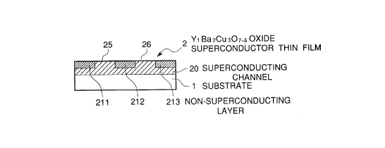
As shown in Pigure ]A, there is pl.,pal~d a substrate 1 having an
YIBa2Cu3O7~ oxide su~ereo.-~uctor thin film 2 formed on its principal
surface thereof~ A c-axis orient~ted thin film is preferably deposited,
since the c-axis orientated thin film has a large critical current density in
dle direction in parallel to the SU~ al~ surface~
The Y~13a2Cu3O7 ~ oxide ~llp~rcol.ductQr ~in film 2 having a
thi(lrn~ss of for example 400 ~ o~ te.~ is deposited on the principal
-: surface of the ~ul sl-~utc 1 by for example an off-axis slJul~etiug, a reactive
evaporation, an MBE (molecular beam epitaxy), a CVD, etc~ The
condition of forming the c-axis orientated YlBa2Cu3O7 ~ oxide
su~..;~ nd~lGtor thin film 2 by off-axis s~.lue~ing was as follows:
S~u~ g Gas Ar: 90%
~ ~2: 10%
~ Total pressure S x 10-2 Torr
T~ ~r~ture of the substrate 700~C
~,
10 -
... . .
" ~ :
, . . .
.: . . .
2~77047
Then the YlBa2Cu307 ~ oxide ~l~yerconductor thin film 2 is heated
at a temperature of 375~C in high vacuum envirolllllel~l under the
background p~s~llre of less than 1 x 10⁹ Torr, The condition of the
heat~ ,a~...f l~ was as follows:
Pressure S1 x 10-9 Torr
Te.l,~e.&lu~ of the sl~bstr~te 375~C
Heating dur~tioil 10 ~ t~s
After ~e heat-treatn ent, the surface portion having a thickness of
15 nqno~l~cte~s of the YlBa2Cu3O~.~ oxide supe~conductor thin film 2 is
changed into a non-~up~lcolld~c.tit~g layer 21 formed of YIBa2Cu3O7 e
(~ < ~ < 7) non-superconductin~ oxide, as shown in Figure lB. Lower
portion of the YIBa2Cu307.~ oxide superconductor thin film 2 becomes a
~' ~u~r~o~ductinE ch~nnel 20.
'- The.ea~r, as shown in Figure lC, photoresist layers 41, 42 and 43
are formed on the YlBa2Cu3O7.g oxide superconductor thin film 2,
namely on the non-~u~rco~ ctin~ layer 21, se~ dt~ly from each other.
Then the YIBa2Cu3O7.g oxide su~e~onductor thin film 2 is heated at a
le.,lpc,atul~ of 375~C in an oxygen atmosphere. Th,e condition of the
heat-~l~O~...c nl was as follows:
~l~si,ul~ of O2 1 x 10⁻² Torr
Te~ eral~lre of the substrate 375~C
Heating c~ ti~n 10 lnin~1t~s
During the heat tre~tmP-nt, oxygen penetrates into the exposed
surface portions 25 and 26 of the non ~u~,cl~ol,~cting layer 21 so that the
Ba2Cu3O7 E non-su~ercol-duGtin~ oxide of the portions changes into the
. .~ .
~, YIBa2Cu3O7.~ oxide supercor~ductor. After the heat treatment, the
, portions 211, 212 and 213 under the photoresist layers 41, 42 and 43
. ................................... .
;".' '11-
.,
.
.
,
2~77~47
remain non-superconducting, and the surface superconducting portions 25
and 26 u~ cl to the ~-,~rc~ cting channel 20, as shown in Figure lD.
The recovered superconclucting portions 25 and 26 are patterned into
bi~ r shapes by fonning the photo.e~is~ layers 41, 42 and 43 into ~e
iplocal shapes so that the YlBa2Cu307~ oxide supe.c~ ctor thin film
2 has a Sup~OI d~lctin~ contact region at the surfR~e.
Finally, as shown in Figure lE, the photoresist layers 41, 42 and 43
are removed, if necessary, and the superconducting thin film is
completed. In this connection, it is preferable that the method for
removing the photoresist layers 41, 42 and 43 does not affect the
YlBa2Cu307.~ oxide su~lcondllctQr, for example a dry etching process.
The surface superconducting portions 25 and 26 of the
YlBa2Cu3O7~ oxide su~elcollductor thin film 2 manufactured in
accordance with the present invention is not degraded, since no
photoresist layer is formed on the portions. Therefore, both the
supe~o~dl)Gtin~ e~ nn~.l 20 and the surface supercon~hlctin~ portions 25
and 26 of the YlBa2Cu3O7.~ oxide s~.perco,~ductor thin film 2 have high
quality ~upc.col~ductivity.
As explained above, if the superconducting thin film is
manufactured in accordance ~ith the above mentioned process, a
superconducting pattern can be formed without spoiling the
~upc,col~dnctivity of the oxide supercol-ductor. Accordingly, it is easy to
a.-ufacture the supercon~ucti~ pattern with good repeatability, and the
l.,ractured su~rco~ cting pattern has stable characteristics.
:''
, . . .
.~.
- 12-
:,- t
:
.,
.,
2077047
Embodiment 2
Referring to Figures 2A to 2E, a second embodiment of the process
in accordance with the present invention for manufacturing the
supc~Q~ JGtin~ device will be described.
As shown in Figure 2A, there is prepared a substrate 1 having an
Y~Ba2Cu3O7 ~ oxide ~u~rcol~ductor thin film 2, similar to the ~ul)s~ldte 1
and the YlBa2Cu3O7.g oxide superconductor thin film 2 of the
bodil"ent 1. The YIBa2Cu307.~ oxide superconductor thin film 2
having a thickness of for example 20 nanometers is deposited on the
principal surface of the substrate 1 by for example an off-axis s~ lel;ng~
The off-axis sy~ eling is performed under the same condi~on as that of
the Emb~dime~
Then dle YlBa2Cu307.~ oxide ~ulJelcollductor thin film 2 is heated
at a t~lpe~ ule of 375~C under high vacuum of less than 1 x 10⁻⁹ Torr~
The con~lition of the heat-treatnlent is same as d~at of the Embodiment 1~
After the heat-treatment, the surface portion having a thi~n~ss of
15 n~ e,~ of the YlBa2Cu30~.~ oxide sl~perconductor thin film 2 is
changed into a non-supel~col~d~lctin~ layer 21 fo~ned of YlBa2Cu307.E
(~ < ~ < 7) non-~up~ rcol~ducting oxide, as shown in Figure 21~ Lo~ver
portion of the YlBa2Cu307.~ oxide supercontluctor thin film 2 becomes a
su~co,.d.lctin~ ch~nn~l 20.
. .
.i The.~,ar~r, as sho~,vn in Figure 2C, photoresist layers 41, 42 and 43
are fo~ cd on the YlBa2Cu307.~ oxide superconductor thin film 2,
namely on the non-superco~d~lctir ~ layer 21, separately from each other.
Then, Au layer is deposited on the YIBa2Cu307.~ oxide
sul,crcoQdnctor thin ~llm 2 by a vacuum e~poralion method. After then,
dle photoresist layers 41, 42 and 43 are removed so ~at gate electrodes
:
- 13-
2077047
51 and 52 are fonned on the non-supercollducting layer 21, as shown in
Figure 2D. The non-sup~-col~ducting layer 21 is little degraded by a
hotGIGsisl developer and photoresist remover during the process.
Finally, a Y~Ba2Cu3O7.g oxide su~crcol~ductor thin film is depo~ited
on the non-superconducting layer 21 by an off-axis sputtering so that
sulx~ol-~lucting regions 31, 32 and 33 are formed, as shown in Figure
2E. This YlBa2Cu307.~ oxide supercon~ ctQr thin film is preferably
a-axis ol;c,ll~d While the YlBa2Cu3O7.g oxide sl.perco.lductor thin film
is deposited, oxygen penetrates into portions of the non-~ul)erconducting
layer 21 excluding portions under the gate electrode 51 and 52. The
YlBa2Cu307.E portions 31, 32 and 33 of the non-superconduc~ing layer
21, into ~vhich oxygen penetrates, changes into the YlBa2Cu307.~ oxide
~uperconductor so that gate ins~ t~rs are formed only under the gate
ele~l,odes 51 and 52 and the ~upercol~(lucting regions 31, 32 and 33 are
electrically connPcte~l to the supe~col)d~lcting channel 20.
Then, YlBa2Cu307 ~ oxide ~upercol~vctor thin films deposited on
the gate electrodes 51 and 52 are removed so that the superconducting
device has a planar sur~ace, if l~cess~
~;' In the superconducting device m~n~lf~ctured by the above
.. . .
mentioned process, the superc~,ducting current flowing through the
~upe~o~dvcting charmel 20 between the ~rco~-ducting region 31 and
32 is controlled by a voltage applied to the gate electrode 51, and the
su~,,co~ld.~cting current flowing through the supercol-~uctin~ ch~nnel 20
l~l.. een the ~u~ollducting region 32 and 33 is controlled by a voltage
applied to the gate electrode 52. Therefore, the superco,lducting device
co~ ules a kind of super-FET.
....
.
- 14-
:,..
, .
20770~7
As explained above, if the above mentioned super-FET is
manufactured in accordance with the above mentioned process, it becomes
easy to form ~e stacked structure in which ~e gate insu1 ~or is stacked on
~e superco~ rting channel formed of an oxide sup~rco,lductor th~n film.
In addition, since the upper surface of the superconductor thin fi}m is
pla~&,;~d, it becon~r easy to form cQn~GtQr wirings in a later process.
Accordingly, it is easy to manufacture the super-FET with good
reye~t~bility~ and the manufactured super-FET has a stable perfonn~n~e
F.mho~im~nt 3
Referring to Figures 3A to 3H, a third embo~iment of the process
in accordance with the present invention for manufacturing the
super-FET will be described.
As shown in Figure 3A, there is prepared a substrate l, similar to
the substrate l of the Embodiment l.
As shown in Figure 3B, a c-axis orie-n~ted YlBa2Cu307.~ oxide
~uFerconductor thin film 2 having a thickness of for example 20
l-a~ rt~.~ is deposited on the ~-incipal sur~ace of the SIl~Slldt~ 1 by for
example an off-axis sputtering. The off-axis ~yultel;ng is pelro~ ed
under the same condi~ion as that of the Emboflimrnt l.
- Then the YIBa2Cu3O7~ oxide ~ùpe~ol ductor thin film 2 is heated
at a telllpelature of 375~C under high vacuum of less than l x lo-9 Torr.
The con~1ition of the heat-l-e~1n~ is same as that of ~e EmbodimPn~ l.
~' After the heat-~.. r~ , the suRace portion having a ~hirlrn.oss of
15 nanolnet~.~ of ~e Y~Ba2Cu3O1.~ oxide superconductor thin ~llm 2 is
~' changed into â non-super~onducting layer 21 formed of Y~Ba2Cu3O7 ~
- (~ < ~ < 7) non-~u~reol-ducting oxide, as shown in Figure 3C. Lower
.. .
:....;
- 15-
. .
2~770~7
portion of the YlBa2Cu307.~ oxide su~er~onductor thin film 2 becomes a
sul)creollduc~ing ch~nn~l 20.
Thereafter, as shown in Figure 3D, a Si3N4 thin film 90 is deposited
on the YlBa2Cu3O7 ~ oxide su~crcol-d~lctor thin film 2, namely cn the
non-su~lco~d~l~tin~ layer 21. While the Si3N4 thin film 90 is deposited,
Si dirr lses into the non-su~e~ol-d~Gtin~ layer 21. However, the quantity
of ~e di~sillg Si is slight so that the dir~usil~g Si does not affect ~e non-
sUyereon(1~1cting layer 21. Instead of Si3N4, sio2 Call also be used.
Then, an Au film 50 is deposited on the Si3N4 thin ~llm 90 by a
vacuum evaporation medlod, as shown in Figure 3E. The Au film 50 and
the Si3N4 thin film 90 are selectively etched so as remove all of the Au
film 50 and the Si3N4 thin film 90 excllldir~g a portion which becomes a
gate electrode S and a gate incul~or by an unisotropic etching process, for
ex~mrlç a reactive ion etching ~ cess or an ion milling using Ar-ions, as
shown in Figure 3F.
After then, side inculating members 91 and 92 of Si3N4 are formed
at ~e both sides of dle gate electrode 5, as shown in figure 3G. Finally,
~. ~
an a-axis orient~ted YIBa2Cu3O7.~ oxide suycrco~ tQr thin film having
~; a thic~n~ss of 800 n~nQmeterS is deposited on the non-~u~reonductiDglayer 21 by an off-axis s~lt~ g so that a ~upe~on~uc~ing source region
, , ,
3 and a superconducting drain region 4 are formed, as shown in
; Figure 3H.
The condition of fol~ g the a-axis orienlated YlBa2Cu3O7 ~ oxide
- . sup~rcol-d~lctor thin film by off-axis ~yullelillg was as follows:
Spu~ g Gas Ar: 90%
O2: 10%
,.
- Total pressure 5 x 10⁻² Torr
, . . .
.
- 16-
, .... .
.
2~770~7
Temperature of the substrate 630~C
W~hile the a-axis orientnte~ YIBa2Cu307 ~ oxide s.lperconductor thin
film is deposited, oxygen penetrates into portions of the non-
supe~co~ ncting layer 21 e~ch~dinp portions under the gate electrode 5.
The c-axis o.;~ ed YlBa2Cu307.~ portions of the non-su~~rcol~ducting
layer 21, into which oxygen pe.lctlates, ch~r~ges into the Y~Ba2Cu3O~.~
oxide ~u~..;ondvr~tor so that gate insulators are formed only under the
gate electrode 5 and the superconducting source region 3 and
superconducting drain regiorl 4 are electrically connected to the
~uycrco~lucting channel 20.
Then, the a-axis oriç~t~e~l YlBa2Cu307.~ oxide su~rcol,d~lctQr thin
films ~eposited on the gate electrode S is removed so that the
su~rcon~lctin~ device has a planar surface, if n~.cess~ry.
As explained above, if the above mentioned super-F~iT is
ma~vf~rt~red in accordance with the above mentioned process, it becomes
easy to form the stacked structure in which the gate in.~ul~tor is s~ac~ on
the su~lc~d.lcti~ channel formed of an oxide supercon~ ctor thin film.
In addition~ since the upper surface of the supercol-d~lctor thin film is
planarized, it become easy to form con~uc~Qr wirings in a later process.
Accordingly, it is easy to manufacture the super-FET with good
repeatability, and dle m~nufactllred super-FET has a stable perforrn~nre.
In the above mentioned embo~ime1~ts~ the oxide sul,creo.-~ctor thin
film can be formed of not only the Y-Ba-Cu-O type compound oxide
supc-conductor material, but also a high-Tc (high critical t~ perature)
oxide su~co~1ductor material, particularly a high-TC copper-oxide type
compound oxide ~u~e.colU~uctQr material, for example a Bi-Sr-Ca-Cu-O
~0770~7
t,vpe compound oxide superconductor material, and a Tl-Ba-Ca-Cu-O type
compound oxide su~,coi-~luctQr material.
The invention has thus been shown and described wi~ reference to
the specific embo~imP-nt Hc-.e~cr, it should be noted that the present
invention is in no way limited to the details of the illustrated structures
but convells and modifications may be made within the scope of the
appel ~i claims.
18 -