Note: Descriptions are shown in the official language in which they were submitted.
2 û 7 ~ 2 0 4
BACKGROUND OF THE INVENTION
Thls lnventlon relates to hlgh-speed current
swltchlng clrcuitry and, more partlcularly, to a current
swltchlng tree havlng cascaded sets of swltchlng clrcults wlth
an lnput set belng drlven at a constant, flxed sampllng rate
and wlth means for reduclng the effectlve sampllng frequency
of the tree whlle malntalnlng sald constant, flxed sampllng
rate.
As descrlbed ln the aforementloned speclflcatlon, a
hlgh-speed current sampllng clrcult ls formed as a swltchlng
tree comprlsed of successlve, cascaded sets of swltchlng
clrcults, wlth each succeedlng set belng supplled wlth
sampllng pulses of reduced frequency. Thls swltching tree
permlts the sampllng at a satlsfactorily hlgh rate of an lnput
slgnal havlng hlgh frequency components, whlle enabllng each
sample whlch ls produced at the aforementloned hlgh rate to be
processed at a relatlvely lower speed. Thus, current samples
can be produced on the order of about 1 GHz; but each such
sample may be stored temporarlly and then dlgltlzed at a
relatlvely low rate well wlthln the operatlng capabllltles of
lnexpenslve analog-to-dlgltal (A/D~ converters.
60939-1543
,
207720~
PATENT
455610-2110
1 Accurate operation of such high-speed switching
2 circuits is dependent, to a large degree, upon the stability of
3 the clock generator used to produce the sampling pulses supplied
4 to the respective sets in the switching tree. Typically, a
crystal oscillator is used as a reference clock source because it
6 exhibits a fixed, stable frequency at high repetition rates.
7 Usually, circuit components are selected on the basis of their
8 ability to switch quickly and accurately, without saturation and
g without being susceptible to drift, delays and phase shifts at
high operating speeds. Good circuit design thus takes into
11 account various capacitive components of the circuits being used.
12 While the fabrication of such circuits as an integrated circuit
13 minimizes deleterious influences at ~igh operating speeds,
14 optimum circuit design nevertheless is premised upon a particular
operating rate at which the switching tree is driven.
16 Accordingly, it has been found that it is not an easy
17 matter to operate an expensive, high-speed switching tree at low
18 speeds because of the design considerations upon which the
19 circuit design was based. That is, less than optimum performance
is attained if the crystal oscillator normally used to supply
21 6ampling pulses to the switching tree is replaced by an
22 oscillator exhibiting a lower repetition rate. Likewise, a
23 switching tree designed for high operating speeds may not operate
-2-
207720~
PATENT
455610-2110
1 satisfactorily if the normally high repetition rate of the clock
2 signals generated by the aforementioned crystal oscillator is
3 divided by conventional frequency dividers, programmable
4 dividers, or the like.
Although separate switching trees may be purchased for
6 use at respectively different frequencies, with each tree being
7 designed to operate at a respective one of those frequencies, the
8 stockpiling of several switching trees, each for use at a
9 separate operating speed, is redundant and expensive. Hence,
there has been a need to provide a switching tree operable at
11 various different effective sampling rates without sacrificing
12 performance or operating characteristics regardless of the
13 operating speed at which the sampling tree is used.
14 To increase the sampling speed of the aforementioned
switching tree, it has been proposed to supply an input signal to
16 be sampled to plural phases of switching trees, each operable at
17 the same sampling rate but at respectively different phases. For
18 example, if three phases of sampling trees are used, with the
19 input set of each phase being driven at a sampling rate f f8~ an
input signal supplied to these three phases is sampled at an
21 effective sampling frequency of 3f8. It is important, however,
22 particularly if the input signal exhibits very high freguency
23 -components, such as transients, that the respective phases of the
2~7720~
PATENT
455610-2110
1 sampling clock pulses supplied to these switching trees be
2 maintained within strict limits. For instance, in the
3 aforementioned example wherein three phases of switching trees
4 are used, the sampling clock pulses should be supplied at 0,
-5 120 and 240 to these respective phases. It is difficult,
6 however, to provide fine phase adjustments at the very high
7 sampling frequencies exhibited by the sampling clock pulses.
8 OBJECTS OF THE INVENTION
9 Therefore, it is an object of the present invention to
provide improved high-speed sampling circuitry which overcomes
11 each of the aforenoted disadvantages and drawbacks.
12 Another object of this invention is to provide a high-
13 speed switching tree supplied with an input sampling clock
14 exhibiting a fixed, stable frequency, and including a sample
skipping circuit which operates to reduce the effective sampling
16 frequency of the switching tree while maintaining the fixed,
17 stable frequency of the input sampling clock.
18 A further object of this invention is to provide a
19 switching tree designed for high frequency operation yet operable
at significantly lower effective sampling rates, thus increasing
21 the versatility and usefulness of that switching tree.
22 An additional object of this invention is to provide a
23 plural phase switching tree with each phase being driven at the
207~20~
PATENT
455610-2110
1 ~ame input sampling rate, wherein the respective phases of the
2 input sampling clocks are accurately adjustable even though such
3 ~ampling clocks operate at very high repetition rates in excess
4 of 500 MHz.
Another object of this invention is to provide a delay
6 adjustment circuit having particular utility in a plural phase
7 switching tree of the aforenoted type.
8 A still further object of this invention is to provide
9 improved control over a switching tree whose output samples are
stored, read out and displayed on a device which operates
11 asynchronously of the switching tree.
12 Various other objects, advantages and features of the
13 present invention will become readily apparent from the ensuing
14 detailed description, and the novel features will be particularly
pointed out in the appended claims.
16 SUMMARY OF THE INVENTION
17 In accordance with this invention, a current switching
18 tree is comprised of successive, cascaded sets of current
19 sampling circuits, each set operating at a respective one of
different repetition rates, with an input set being driven at a
21 fixed, high frequency. The effective sampling rate of the
22 ~witching tree is reduced by a sample skipping circuit
23 ~interconnected between successive levels of the switching tree,
-5-
2077~04
.
PATENT
455610-2110
1 for example, between the input level and a succeeding
2 intermediate level. The sample skipping circuit is selectively
3 energized to pass some samples and to block others.
4 As a feature of this invention, a sequencing circuit
-5 supplies those samples which are passed by the sample skipping
6 circuit to differing switching circuits in, for example, an
7 intermediate level from which the samples are coupled to storage
8 devices at the output level, the sequencing circuit functioning
9 to assure that substantially all of the storage devices in the
output level are used, even though certain samples normally
11 destined for those devices may be blocked.
12 As another feature of this invention, plural phases of
13 the aforementioned switching tree are used to increase the
14 effective sampling rate at which an input signal is sampled, even
though a common sampling clock may be used to produce sampling
16 clock pulses for all of the phases. An adjustable delay circuit
17 is providPd for delaying the sampling clock pulses produced by
18 the sampling clock, thereby establishing predetermined phases of
19 sampling clock pulses of the same frequency for use by the
respective phases of switching trees.
21 As an aspect of this feature, the adjustable delay
22 circuit is comprised of two differential circuits for receiving
23 pulse signals that are delayed with respect to each other, both
20772 ~ 4
dlfferentlal clrcults belng supplled wlth current from a
current source, and whereln a current ad~ustment clrcult
operates to vary the current supplled by sald source to one of
the dlfferential clrcults relatlve to the current supplled to
the other dlfferentlal clrcult, thereby produclng an output
pulse at a tlme of occurrence whlch varles as a function of
the current ad~ustment clrcult.
The invention may be summarized, according to one
aspect, as current switchlng apparatus comprlslng: a plurallty
of cascaded sets of current sampllng means, lncludlng an lnput
set and an output set, each set lncludlng at least one current
swltchlng clrcuit havlng an lnput and plural outputs and
responsive to clock signals of dlfferent repetltlon rates
supplied to respectlve sets for swltchlng to selected outputs
at a sampllng frequency a current sample applled to sald
lnput, the lnput of a current swltchlng clrcult ln one set
belng coupled durlng normal operation to a respectlve output
of a current swltchlng circult in a preceding set; a clock
source for supplying a clock slgnal of flxed frequency to sald
lnput set and of respectlvely dlfferent frequencles to the
other sets; and sample sklpplng means for reduclng an
effectlve sampllng frequency of at least one of sald current
swltchlng clrcults whlle malntainlng the fixed frequency of
said clock slgnals supplled to said input set.
According to another aspect, the present invention
provldes current swltchlng apparatus comprlsing: a plurallty
of cascaded sets of current swltchlng means, lncluding an
lnput set and an output set, each set lncludlng at least one
60939-1543
.
20772 ~ 4
current swltchlng clrcult havlng an lnput and plural outputs
and responslve to clock slgnals supplled thereto for swltchlng
a current applled to sald lnput to selected ones of sald
outputs, the lnput of a current swltchlng clrcult ln one set
belng coupled to a respectlve output of a current swltchlng
clrcult ln a precedlng set to recelve a current therefrom
durlng normal operatlon; current dumplng means coupled to
predetermlned outputs of the current swltchlng clrcults ln a
predetermlned set for selectlvely dumplng current swltched
thereto ln response to predetermlned transltions of sald clock
slgnals and a clock generator for generatlng sald clock
slgnals.
Accordlng to yet another aspect, the lnventlon
provldes plural phase current swltchlng apparatus comprlslng
plural phases of current swltchlng tree clrcults, each phase
lncludlng an lnput set of current swltchlng clrcults supplled
wlth sampllng clock pulses, an output set of current swltchlng
clrcults and at least one lntermedlate set of current
swltchlng clrcults, each set havlng an lnput and plural
outputs wlth the lnput of one set belng coupled to a
respectlve output of a precedlng set; plural phase clock
generatlng means for generatlng plural phases of sampllng
clock pulses of flxed frequency and lncludlng ad~ustable delay
means for delaylng a respectlve phase of sampllng clock pulses
by an ad~ustable delay and thereby establlshlng predetermlned
phases of sampllng clock pulses of the same frequency and
dlfferent phases; means for supplylng sald plural phases of
sampllng clock pulses to the lnput sets of current swltchlng
- 7a -
60939-1543
2077~ ~ 4
clrcults ln sald plural phases of current swltchlng tree
clrcults, respectlvely; plural phases of swltchlng pulse
generatlng means for derlvlng from sald plural phases of
sampllng clock pulses respectlve phases of swltchlng pulses of
dlfferent repetltlon rates, each phase of swltchlng pulses
belng supplled to a respectlve phase of current swltchlng tree
clrcults for drlvlng the lntermedlate and output sets thereln
at sald dlfferent repetitlon rates; and plural phases of
sample sklpplng means, each coupled to a respectlve phase of
current swltching tree clrcults for reduclng an effective
sampllng frequency thereof whlle malntalnlng the flxed
frequency of the sampllng clock pulses supplled to the input
set of current swltchlng clrcults lncluded ln sald respectlve
phase of current swltchlng tree clrcults.
BRIEF DESCRIPTION OF THE DRAWINGS
The followlng detalled descrlptlon, glven by way of
example, wlll best be understood ln con~unctlon wlth the
accompanylng drawlngs ln whlch
FIG. 1 ls a schematlc dlagram of one embodlment of a
swltchlng tree used wlth the present lnventlon;
FIG. 2 ls a schematlc dlagram of another embodlment
of a swltchlng tree for use wlth thls lnventlon;
FIGS. 3A-3U are tlmlng dlagrams whlch are useful ln
understandlng the operatlon of the embodlment shown ln FIG. l;
FIGS. 4A-4M are tlmlng dlagrams whlch are useful ln
understandlng the operatlon of the embodlment shown ln FIG. 2;
FIG. 5 ls a schematlc dlagram of a portlon of the
embodlment shown ln FIG. 2;
- 7b -
60939-1543
~ -....
. ~ "
207720~
PATE~T
455610-2110
1 FIGS. 6A-6E are waveform diagrams which are useful in
2 understanding the manner in which samples are written into and
3 read out of storage elements in the embodiment of FIG. 5;
4 FIG. 7 is a schematic diagram illustrating one
embodiment of the present invention;
6 FIGS. 8A-8C are waveform diagrams which are useful in
7 understanding the operation of the present invention;
8 FIG. 9 is a block diagram illustrating another aspect
9 of the present invention;
FIGS. lOA-lOH are waveform diagrams which are useful in
11 understanding the manner in which sampling clock pulses are
12 produced for the embodiment shown in FIG. 9; and
13 FIG. 11 is a schematic diagram of a preferred
14 embodiment of a delay adjustment circuit used to generate
sampling clock pulses in the embodiment of FIG. 9.
16 DETAILED DESCRIPTION OF CERTAIN PREFERRED EMBODIMENTS
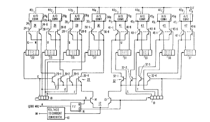
17 Referring now to the drawings, FIG. 1 illustrates one
18 embodiment of high-speed sampling apparatus in which the present
19 invention finds ready application. The illustrated apparatus
includes plural cascaded sets, or levels, of sampling circuits
21 including an input set, or level 12, an output set, or level,
22 including sampling circuits 24, 26, 28, 30, 41, 43, 45, and 47
23 and an intermediate set, or level, comprised of sampling circuits
20772o'l
PATENT
455610-2110
1 20 and 32. These sets are seen to be cascaded from the input set
2 to the intermediate set to the output set in the form of a
3 sampling "tree". Input set 12 is comprised of a pair of
4 switching elements 13 and 14. In one embodiment, the switching
elements are comprised of transistor devices; and as shown in
6 FIG. 1, such transistor devices may, for example, be bi-polar
7 transistors. It will be appreciated by those of ordinary skill
8 in the art that other types of transistor devices which are
g capable of operating at high switching frequencies may be used;
and, moreover, the switching elements need not be limited solely
11 to transistor devices. However, in the interest of brevity and
12 simplification, it is assumed, for the purposes of discussion,
13 that the illustrated switching elements are formed of transistor
14 switching devices.
Input set 12 of switching devices 13, 14 includes a
16 common-connected input, here illustrated as the emitter
17 electrodes of transistors 13 and 14, adapted to be supplied with
18 an input signal to be sampled. An input sample is obtained by
19 actuating the switching device in response to a sampling signal
supplied thereto. In particular, the sampling signal, such as a
21 sampling pulse, supplied to the base electrode of, for example,
22 transistor switch 14 renders this transistor switch conductive so
23 -as to couple the signal supplied to the emitter electrode thereof
2~7720~
PATENT
~ 455610-2110
1 to its collector electrode. Switching devices 13 and 14 are
2 operated, or actuated, at the same sampling rate, but at
3 different respective phases. In particular, the switching
4 devices are actuated alternatively.
The sampling pulses supplied to input set 12 are
6 derived from a clock source (not shown) capable of generating
7 stable, high frequency clock pulses on the order of, for example,
8 1,000 MHz. A frequency divider 16, formed of, for example, a
9 flip-flop circuit, is coupled to the clock source and functions
to divide the freguency of the clock pulses by the factor 2. As
11 is conventional, flip-flop circuit 16 includes a pair of outputs
12 Q and Q, these outputs supplying sampling pulses at, for example,
13 500 MHz in opposite phases. Flip-flop circuit 16 may be thought
14 of as a single stage shift register.
Since input set 12 of switching devices 13, 14 is
16 comprised of only two switching devices in the example described
17 herein, the input set is provided with two outputs. These
18 outputs are coupled to respective inputs of the next set of
19 sampling circuits. In the illustrated embodiment, this next set
is comprised of the intermediate set, or level, of sampling
21 circuits 20 and 32. Sampling circuits 20 and 32 may be thought
22 of as separate groups of switching devices. These groups are of
--10--
207720~
PATENT
455610-2110
1 substantially identical construction, and only the group which
2 comprises sampling circuit 20 need be described in detail.
3 In the illustrated example, sampling circuit 20 is
4 comprised of four switching devices 20-1, 2-2, 20-3 and 20-4,
respectively. Although any desired number of switching devices
6 may be used, it is preferred herein to utilize four switching
7 devices in sampling circuit 20. These switching devices may be
8 similar to aforedescribed switching devices 13 and 14; and in the
9 embodiment described herein, switching devices 20-1... 20-4 are
diagrammatically represented as transistor elements. The input
11 of sampling circuit 20 is comprised of the common-connected
12 inputs, or emitter electrodes, of switching devices 20-1, 20-2,
13 20-3 and 20-4. As illustrated, this input is coupled to the
14 output, or collector electrode, of switching device 14 included
in the input set 12 of sampling circuits. Similarly, the input
16 of sampling circuit 32 is comprised of common-connected emitter
17 electrodes coupled to the output, or collector electrode, of
18 switching device 13.
19 Switching devices 20-1, 20-2, 20-3 and 20-4 are
actuated, or rendered conductive, in sequence. The actuation, or
21 conductivity, of these switching devices is determined by the
22 successive phases of sampling pulses supplied thereto by a source
23 ~of intermediate level sampling pulses 18. In a similar manner,
207720~
PATENT
455610-2110
1 the respective switching devices included in sampling circuit 32
2 are actuated, or rendered conductive, in sequence, by the
3 respective phases of sampling pulses supplied thereto from source
4 19. Sources 18 and 19 may be thought of as suitable sampling
pulse (or clock pulse) generators, each coupled to receive a
6 respective phase of the first-level sampling pulses. More
7 particularly, each of sampling pulse sources 18 and 19 is
8 comprised of a plural-stage shift register adapted to receive a
9 sample pulse generated by flip-flop circuit 16 to propagate a
pulse through the respective stages thereof. Each stage of shift
11 register 18 is coupled to a respective control terminal, or base
12 electrode, of switching devices 20-1, 20-2, 20-3 and 20-4.
13 Likewise, each stage of shift register 19 is coupled to a
14 respective control terminal of the switching devices included in
sampling circuit 32. Thus, as a pulse is shifted from stage-to-
16 stage in shift register 18 in response to each sampling pulse
17 supplied thereto from flip-flop circuit 16, successive ones of
18 the switching devices included in sampling circuit 20 are
19 actuated, or rendered conductive. It is appreciated that when a
switching device is actuated, a signal supplied to the input
21 thereof, that is, the signal supplied to the common-connected
22 inputs of the switching devices, is switched, or transferred, to
23 -the output of that actuated switching device.
-12-
207720~
PATENT
455610-2110
1 The output of each switching device included in
2 sampling circuit 20 is coupled to the input of a respective
3 sampling circuit included in the output set, or level.
4 Similarly, each output of sampling circuit 32 is coupled to the
input of a respective sampling circuit included in the output
6 set, or level. In the interest of brevity, only output sampling
7 circuits 24, 26, 28, and 30 are described in detail. In the
8 example described herein, each sampling circuit included in the
9 output set, or level, is comprised of eight individual switching
devices. Any other number of switching devices may be included
11 in sampling circuits 24, 26, 28, 30, 41, 43, 45, and 47, as
12 desired.
13 Sampling circuit 24 is illustrated in detail, and the
14 switching devices 24-1 .... 24-8 included therein have their
inputs, or emitter electrodes, connected in common to the output,
16 or collector electrode, of switching device 20-1 included in
17 sampling circuit 20 of the preceding set, or level. Similarly,
18 the inputs of the switching devices included in sampling circuit
19 26 are connected in common to the output of switching device 20-
2, the inputs of the switching devices included in sampling
21 circuit 28 are connected in common to the output of switching
22 device 20-3, and the inputs of the switching devices included in
23 sampling circuit 30 are connected in common to the output of
2077~
PATENT
455610-2110
1 ~witching device 20-4. Likewise, the inputs of the ~witching
2 devices included in sampling circuit 41 are connected in common
3 to the output of switching device 32-1, and the remaining
4 sampling circuits 43, 45 and 47 are similarly connected to
switching devices 32-2, 32-3 and 32-4, respectively.
6 The control terminals, or base electrodes, of switching
7 devices 24-1 .... 24-8 are coupled to a source 22 of sampling
8 pulses. Preferably, source 22 is comprised of a plural-stage
9 shift register whose input is coupled to a predetermined stage of
shift register 18. In the illustrated embodiment, the input of
11 shift register 22 is coupled to the output of the first stage of
12 shift register 18. In response to each sampling pulse produced
13 at the first stage of shift register 18, shift register 22
14 propagates a pulse from one stage therein to the next adjacent
stage. The plural stages of shift register 22 are coupled to
16 respective control terminals of switching devices 24-1 ... 24-8
17 to sequentially actuate, or render conductive, those switching
18 devices in response to the propagating, or shifting, of a pulse
19 through the shift register.
In a similar manner, the control terminals of the
21 ~witching devices included in sampling circuit 26 are coupled to
22 the respective stages of a shift register 23 whose input is
23 coupled to, for example, the second stage of shift register 18.
-14-
2~77204
PATENT
455610-2110
1 Likewise, the control terminals of the switching devices included
2 in sampling circuit 28 are coupled to the respective stages of a
3 shift register 25 whose input is coupled to the third stage of
4 shift register 18. Finally, the control terminals of the
switching devices included in sampling circuit 30 are coupled to
6 the respective stages of yet another shift register 27 whose
7 input is coupled to the fourth output of shift register 18. The
8 respective stages of shift register 19 are coupled to similar
9 shift registers 31, 33, 35 and 37, whose stages, in turn, are
coupled to the control terminals of the switching devices
11 included in sampling circuits 41, 43, 45 and 47, respectively.
12 The outputs, or collector electrodes, of switching
13 devices 24-1 .... 24-8 included in sampling circuit 24 are coupled
14 to respective output terminals 241 .. ...248 f the sampling
circuit. Likewise, the outputs of the switching devices included
16 in sampling circuit 26 are coupled to respective sampling circuit
17 output terminals 261 ... 268. Similarly, the outputs of the
18 switching devices included in sampling circuit 28 are coupled to
19 respective output terminals 281 ..... 288; and the outputs of the
respective switching devices included in sampling circuit 30 are
21 coupled to output terminals 301 ..... 38 These output terminals
22 of the output set, or level, of sampling circuits are coupled to
23 analog-to-digital (A/D) converting apparatus.
-15-
2077~04
PATENT
~ 455610-2110
In the embodiment illustrated in FIG. 1, each sampling
2 circuit 24, 26, ... included in the output set, or level, is
3 coupled to a respective A/D converter. Preferably, each A/D
4 converter is a so-called "flash" converter of the type available
5 from TRW Inc. and others. As is known to those of ordinary skill
6 in the art, a flash converter is adapted to convert a signal
7 sample level to a corresponding digital signal at a rapid read-
8 out, or cycling, rate. A/D converters 401, 42~ 43~ 44~ 4
9 46~ 47 and 48 have their output terminals connected to a
10 common output. It will be appreciated that the digital signals
11 produced by the A/D converters are supplied to this common input
12 in a predetermined sequence such that there is no interference at
13 the common-connected output terminals. For example, first the
14 digitized signal sample produced ;~y A/D converter 401 in response
15 to the sample provided at output terminal 241 is read out;
16 followed by the reading out of A/D converter 405 of the digitized
17 sample produced in response to the sample provided at output
18 terminal 411. Then, the digitized sample produced by A/D
l9 converter 42 in response to the sample provided at output
20 terminal 261 is read out, followed by the reading out of the
21 digitized sample produced by A/D converter 46 in response to the
22 sample provided at output terminal 431 Hence, the digitized
23 ~amples are read out in accordance with the following sequence:
--16--
2o772o~
PATENT
455610-2110
1 first, all of the digital signals produced in response to the
2 ~amples supplied to the first inputs of the A/D converters are
3 read out successively, then the digital signals produced by the
4 A/D converters in response to the samples supplied to the second
inputs thereof are read out successively, and so on. As a
6 numerical example, eight A/D converters are provided, each having
7 eight separate inputs, thus producing sixty-four successive
8 digitized samples.
9 It is preferred to supply the input set, or level, of
sampling circuits 12 with an input current. This is because
11 currents are switched easily at high speeds by switching
12 transistors, such as bipolar or MOS transistors. Furthermore, a
13 current sample may be stored for relatively long periods of time
14 on simple storage devices, such as capacitors. If a current
sample l is switched, or steered, to a storage capacitor during a
16 brief interval of time ~t, the charge that is deposited onto that
17 capacitor is an exact measure of the average circuit i during
18 that interval:
19 t2
q = J i dt = i ~t
21 ti
22
20772~
-
PATENT
455610-2110
1 Thus, the stored charge is a sample of the current waveform. The
2 time interval ~t may be made very short, such as 1 nsec. or less,
3 thereby enabling accurate sampling of signals having wide
4 bandwidths. Accordingly, a voltage-to-current converter 10 is
-5 coupled to the input of sampling circuit 12. This voltage-to-
6 current converter is adapted to convert an incoming signal
7 voltage to a corresponding current. Then, depending upon the
8 "train" of switching devices which are actuated, or in the
g cascaded sets, conductive, the input current flows through one or
the other of input switching devices 13, 14, and then through one
11 switching device included in the intermediate set, or level,
12 followed by one switching device included in the output set, or
13 level.
14 A timing diagram representing the switched operation of
1~ the various switching devices illustrated in FIG. 1 is shown in
16 FIGS. 3A-3U. FIG. 3A represents the clock pulses supplied to
17 flip-flop circuit 16 at the rate of, for example, 1,000 MHz. It
18 is appreciated that the frequency, or pulse repetition rate, of
l9 the input clock pulses may be any desired frequency capable of
being stably generated. Since flip-flop circuit 16, shift
21 register 18 and shift register 22 each carry out binary frequency
22 division, the frequency of the input clock signal (FIG. 3A) may,
-18-
2077204
PATENT
455610-2110
1 for convenience, be an integral multiple of a binary number, such
2 as 1,024 MHz.
3 Flip-flop circuit 16 functions to divide the frequency
4 of the clock pulses by the factor 2 to produce sampling pulses of
opposite, alternate phases. FIG. 3B illustrates the sampling
6 pulses produced at output Q of flip-flop circuit 16. It will be
7 appreciated that the sampling pulses produced at the output Q is
8 180 out of phase with respect to the sampling pulses shown in
9 FIG. 3B. Thus, transistors 14 and 13 are actuated, or rendered
conductive, alternately.
11 The sampling pulses shown in FIG. 3B are supplied to
12 shift register 18, to trigger the same to propagate a pulse
13 through the respective stages of this shift register. FIGS. 3C-
14 3F represent such propagation; and it is seen that the pulses
provided at the first stage of shift register 18 (FIG. 3C)
16 exhibit the frequency of 125 MHz and a reference phase assumed
17 herein to be 0. The sampling pulses shown in FIG. 3D are
18 produced at the second stage of shift register 18, and are seen
19 to exhibit the same sampling frequency of 125 MHz and a phase
assumed herein to be 90. The sampling pulses shown in FIG. 3E
21 are produced by the third stage of shift register 18; and these
22 sampling pulses are seen to exhibit the frequency of 125 MHz and
23 the phase of 180. Finally, the sampling pulses shown in FIG. 3F
I
-19-
20772~
PATENT
455610-2110
1 are produced by the fourth stage of shift register 18, and
2 exhibit the frequency of 125 MHz and the phase of 270. The
3 cross-hatched areas of the sampling pulse signals illustrated in
4 FIGS. 3C-3F represent the input signal samples that are
S transferred through switching devices 20-1 ... 20-4,
6 respectively, during the duration of each of the respective
7 sampling pulses (FIGS. 3C-3F). Thus, the first sample of the
8 input signal which is produced by switching device 14 (and
9 represented by the cross-hatched area of the first sampling pulse
shown in FIG. 3B) is transferred, or switched, through switching
11 device 20-1 during the first half of the duration of the sampling
12 pulse shown in FIG. 3C. The second input signal sample produced
13 by switching device 14 is transferred through switching device
14 20-2 during the first half of the duration of the sampling pulse
shown in FIG. 3D. The third input signal sample produced by
16 switching device 14 is transferred through switching device 20-3
17 during the first half of the duration of the sampling pulse
18 illustrated in FIG. 3E. Finally, the fourth input signal sample
19 produced by switching device 14 is transferred through switching
device 20-4 during the first half of the duration of the sampling
21 pulse shown in FIG. 3F. Thereafter, the foregoing cycle is
22 repeated.
-20-
20772~
PATENT
455610-2110
1 It is appreciated, from the sampling pulses shown in
2 FIG. 3B, that switching device 13 produces samples during the
3 negative half portions of each cycle of the sample pulses shown
4 in FIG. 3B. Shift register 19 generates respective phases of
sampling pulses, two of which phases are shown in FIGS. 3S and
6 3T. The frequency of the pulses shown in FIG. 3S, as well as the
7 frequency of the pulses shown in FIG. 3T, is equal to 125 MHz,
8 the same frequency as the sampling pulses which are produced at
9 each stage of shift register 18. The cross-hatched portion of
each pulse shown in FIGS. 3S and 3T represents the input signal
11 sample that is transferred through a respective switching device
12 32-1 and 32-2 included in sampling circuit 32 during the duration
13 of the pulses shown in FIGS. 3S and 3T.
14 From the foregoing, it will be appreciated that the
first input signal sample produced by switching device 14 is
16 transferred through switching device 20-1, and then the first
17 sample produced by switching device 13 is transferred through
18 switching device 32-1. Thereafter, the second input signal
19 sample produced by switching device 14 is transferred through
switching device 20-2, and the next sample produced by switching
21 device 13 is transferred through corresponding switching device
22 32-2. Hence, sampling circuits 20 and 32 alternate in
23 transferring samples therethrough, and at each alternation, the
-21-
2077204
PATENT
455610-2110
1 next switching device included therein is actuated. If desired,
2 the switching devices 20-1, 20-2, ... , and 32-1, 32-2, ... , may
3 be actuated in any other sequence or order.
4 Shift register 22 responds to the pulses shown in FIG.
3C to propagate a sampling pulse through the plural stages
6 thereof. As a result, sequential phases, each shifted by 45,
7 are provided at the outputs of the stages of shift register 22,
8 as shown in FIGS. 3G-3N, respectively. It is seen that the
9 frequency of each phase of these pulses is equal to one-sixty-
fourth the input clock frequency. The cross-hatched areas shown
11 in FIGS. 3G-3N represent the transfer of the input signal sample
12 through the respective-switching devices included in sampling
13 circuit 24 during the duration of each respective phase of the
14 sampling pulses supplied to this sampling circuit. FIGS. 30 and
3P represent two successive phases of the sampling pulses
16 supplied from similar shift register 23 to sampling circuit 26.
17 Likewise, FIGS. 3Q and 3R represent two successive phases of the
18 sampling pulses produced by shift register 25 and supplied to
19 sampling circuit 28.
It will be appreciated that sampling circuits 41, 43,
21 45 and 47 to which the respective outputs of sampling circuit 32
22 are coupled are driven by respective, sequential phases produced
23 by shift registers 31, 33, 35 and 37, respectively. FIG. 3U
-22-
2077204
PATENT
455610-2110
1 represents one of these phases as produced by the first stage of
2 shift register 31.
3 In the embodiment shown in FIG. 1, the first input
4 signal sample produced by switching device 14 is coupled through
switching device 20-1 and then through switching device 24-1 to
6 A/D converter 401. Thereafter, the first input signal sample
7 produced by switching device 13 is coupled through switching
8 device 32-1 and then through switching device 41-1 to A/D
9 converter 405. The next signal sample is produced by switching
device 14, and at this time, shift register 18 actuates switching
11 devices 20-2 to couple this sample therethrough and then through
12 the first switching device included in sampling circuit 26. The
13 next signal sample is produced by switching device 13, and this
14 sample is coupled through switching device 32-2 and then through
the first switching device included in sampling circuit 43 to A/D
16 converter 46 The next signal sample produced by switching
17 device 14 is coupled through switching device 20-3 and then
18 through the first switching device included ln sampling circuit
19 28 to A/D converter 403. This alternating sequence is repeated
until all of the first switching devices included in sampling
21 circuits 24, 26, 28 and 30 as well as in sampling circuits 41,
22 43, 45 and 47 have been actuated. Then, the sequence is
-23-
- 2077204
PATENT
455610-2110
1 repeated, and each second switching device included in each of
2 the sampling circuits is actuated successively.
3 It is appreciated that the alternate actuation of
4 switching devices 13 and 14 serves to sample the input signal at
the rate of 1,000 MHz. Because of the illustrated multi-level
6 "tree", each switching device included in the output set, or
7 level of sampling circuits, that is, each switching device
8 included in sampling circuits 24, 26, 28 ... is actuated at the
9 rate of approximately 15 MHz. The A/D converters are capable of
operating at this 15 MHz rate and, in combination, the A/D
11 converters serve to produce digitized samples at the input
12 sampling rate of 1,000 MHz. Hence, FIG. 1 is a schematic
13 representation of one embodiment of a high-speed sampling
14 circuit, each sample being converted to a corresponding digital
representation.
16 In the embodiment of FIG. 1, it may be appreciated
17 that, if desired, any number of intermediate sets, or levels, of
18 sampling circuits may be used. In general, the input set may be
19 thought of as having n outputs (e.g. n = 2); the intermediate set
may be thought of as having x outputs in each group of switching
21 devices (e.g. x = 4 for each of 2 groups); and the output set may
22 ~e thought of as having n.x groups with each group having ~
23 outputs (e.g. y = 8). In the illustrated embodiment only one
-24-
20772~
PATENT
455610-2110
1 intermediate set, comprised of two groups of sampling circuits 20
2 nnd 32, is used. Furthermore, the high-speed sampling circuit
3 may be modified so as to include only an input and an output set
4 of sampling circuits. In this regard, input sampling circuit 12
may be omitted; and the input signal may be coupled directly to
6 the common-connected input of sampling circuit 20 as well as to
7 the common-connected input of sampling circuit 32.
8 Still further, each A/D converter may include a storage
9 device, such as a capacitance element, coupled to a respective
output terminal of the sampling circuit connected thereto for the
11 purpose of storing each sample. The stored sample then may be
12 digitized at an appropriate rate which, for example, may be less
13 than the 15 MHz rate at which the output sampling circuits are
14 driven.
lS In the embodiment shown in FIG. 1, it might be thought
16 that the multi-level tree of sampling circuits is a commutator
17 circuit that is analogous to a single-pole-sixty-four-throw
18 electronic switch. This, however, is not the case. Accurate
19 samples at the high sampling rates described herein are not
attainable if, for example, sixty-four transistors are connected
21 with their emitter electrodes in common and supplied with the
22 input signal to be successively sampled. This is because the
23 very high base-emitter capacitance which obtains by reason of the
207720~
PATENT
4SS610-2110
1 common-connected emitters prevents the respective transistors
2 from being switched, or actuated, at high sampling rates. It is
3 known that the inherent base-emitter capacitance of a transistor
4 is effectively increased as more transistors are connected with
S their emitters in common. Thus, with a large number (e.g. 64) of
6 transistors connected in common, the resultant high capacitance
7 of the common-connected emitters prevents each transistor from
8 responding to the high frequency sampling pulses.
g The sets of transistors shown in FIG. 1 are "matched"
to the frequencies of the particular sampling pulses supplied
11 thereto and, therefore, overcome the aforenoted problem. For
12 example, the input set of switching devices includes a small
13 number (e.g. 2) of transistors connected in common at their
14 emitters. Hence, the effective emitter capacitance of the input
lS set is relatively low and does not degrade the rapid response of
16 these transistors to the very high frequency sampling pulses
17 supplied th~reto. The intermediate set of switching devices is
18 formed of plural (e.g. 2) groups, each group including a somewhat
19 larger number (e.g. 4) of transistors than the input set.
Although this increases the effective emitter capacitance in each
21 group of the intermediate set, the frequency of the sampling
22 pulses supplied thereto is less than the input sampling pulses
23 and, consequently, the transistors are fully enabled to respond
207720~
PATENT
455610-2110
1 thereto. Likewise, the output set of switching devices is formed
2 of groups that include a still larger number (e.g. 8) of
3 transistors, but the resultant increase in emitter capacitance
4 thereof is effectively offset, or compensated, by a lower
sampling pulse frequency. Hence, the transistors in the output
6 set respond satisfactorily to the sampling pulses supplied
7 thereto. Therefore, those groups of transistors having larger
8 effective capacitances, and thus slower response speeds, are
9 supplied with sampling pulses at a slower rate.
Thus, it is seen that the formation of groups of
11 relatively small numbers of transistors reduces the effective
12 capacitance that otherwise would be present if all of the output
13 transistors were connected together. Another advantage of
14 providing groups of transistors is the relative ease with which
clock, or sampling, pulses may be generated. If a single clock
16 generator is used, it is difficult to supply each transistor with
17 its appropriate sampling pulse phase at the correct times.
18 By matching the sampling pulse repetition rates to the
19 response speeds of the respective sets, the levels of the input
signal samples are accurately preserved as those samples
21 propagate through successive ones of the cascaded sets. A sample
22 is not distorted because a particular transistor cannot be
23 -switched fast enough to pass that sample to the next stage.
-27-
20772~1
-
PATENT
- 455610-2110
1 Another embodiment of a high-speed sampling circuit is
2 illustrated in FIG. 2. This embodiment is similar in many
3 respects to the aforedescribed embodiment shown in FIG. 1 and may
4 be fabricated on a single IC chip. In the FIG. 2 embodiment, the
input set, or level, may be supplied with, for example, the
6 samples produced by the intermediate set of the FIG. 1
7 embodiment. The input set of FIG. 2 is illustrated as being
8 comprised of one sampling circuit 60, this sampling circuit being
9 formed of, for example, sixteen individual switching devices 601,
602, 603 .. ....6016. Each of these switching devices may be
11 similar to the aforedescribed switching devices employed in the
12 embodiment of FIG. 1.
13 The inputs, or emitter electrodes, of switching devices
14 601 ....... 6016 are connected in co~on to receive an input signal,
such as successive signal samples as mentioned above.
16 Alternatively, the input signal may be an input current to be
17 sampled and may be generated by a voltage-to-current converter
18 similar to converter 10 of FIG. 1. Each switching device 601
19 6016 is actuated, or rendered conductive, in sequence. To this
effect, a clock generator 62, illustrated herein as a 16-stage
21 ~hift register, is coupled to the switching devices to supply
22 respective phases of clock, or sample pulses thereto. Shift
23 register 62 is coupled to a clock terminal to receive higher
-28-
2~77204
PATENT
455610-2110
1 frequency clock pulses. It is appreciated that shift register 62
2 ~erves to divide the frequency of the input clock signal by the
3 factor 16.
4 Each switching device 601 ... 60l6 included in input
sampling circuit 60 is coupled to a respective sampling circuit
6 included in the output set of sampling circuits. For brevity and
7 simplification, only two of the sampling circuits 70 and 80
8 included in the output set are illustrated. Sampling circuit 70
9 is comprised of, for example, sixteen individual switching
devices 701, 72~ ... 716. Likewise, sampling circuit 80 is
11 comprised of, for example, sixteen individual switching devices
12 801, 802 ... 8016. It will be appreciated that the number of
13 switching devices included in each sampling circuit illustrated
14 in FIG. 2 may be any desired number. Furthermore, the number of
switching devices included in input sampling circuit 60 need not
16 necessarily be equal to the number of switching devices included
17 in each sampling circuit of the output set.
18 The inputs, or emitter electrodes, of the switching
19 devices included in each sampling circuit are coupled in common.
As illustrated in FIG. 2, the common-connected input of sampling
21 circuit 70 is coupled to the output of switching device 60l. The
22 common-connected input of sampling circuit 80 is coupled to the
23 -output of switching device 602. Thus, each output sampling
-29-
2~77204
PATENT
455610-2110
circuit has its common-connected input coupled to a predetermined
2 one of the switching devices included in input sampling circuit
3 60.
4 Switching devices 701 .... 716 are actuated, or
-5 rendered conductive, in sequence, and at a frequency that is less
6 than the frequency at which switching devices 601 ..... 6016 are
7 actuated. Likewise, switching devices 801 ..... 8016 are actuated,
8 or rendered conductive, in sequence and at the same frequency as
g switching devices 701 ... 716. However, the phases at which the
10 switching devices included in sampling circuit 70 are actuated
11 differ from the phases at which the switching devices included in
12 sampling circuit 80 are actuated. Likewise, although not shown
13 in ~IG. 2, the switching circuits included in the .remaining
14 output sampling circuits are actuated, or rendered conductive, at
15 the same frequency as the switching devices included in sampling
16 circuit 70, but at different respective phases. In this regard,
17 each output sampling circuit 70, 80, and so on, is associated
18 with and coupled to a respective shift register 72, 82, etc.
19 These shift registers are of similar construction and, for
20 example, shift register 72 is comprised of a 16-stage shift
21 register, each stage being coupled to the control terminal, or
22 base electrode, of a respective switching device 701 .. ...716.
23 ~The input clock terminal of shift register 72 is coupled to a
--30--
2077204
PATENT
455610-2110
1 predetermined stage of shift register 62. Thus, shift register
2 72 serves to divide the frequency of the sampling pulses supplied
3 thereto from shift register 62 by the factor 16, thereby
4 producing respective phases (0, 22.5, 45, and so on) of output
sampling pulses. Accordingly, switching device 70l is actuated
6 at the 1 MHz rate at, for example, 0 phase, switching device 72
7 is actuated at, for example, 22.5O phase, and so on.
8 Shift register 82 also is a 16-stage shift register;
g and the input clock terminal of shift register 82 is coupled to a
different predetermined stage of shift register 62. Since shift
11 registers 72 and 82 are supplied with pulses having different
12 phases, it is appreciated that the sampling pulses produced by
13 shift registers 72 and 82 also exhibit different phases wi~h
14 respect to each other. In the example illustrated in FIG. 2, the
twelfth stage of shift register 62 is coupled to the input clock
16 terminal of shift register 72 and the thirteenth stage of shift
17 register 62 is coupled to the input clock terminal of shift
18 register 82. If desired, shift registered 72 and 82 may be
19 coupled to any other desired stages of shift register 62.
It will be appreciated that the embodiment of FIG. 2
21 overcomes the problem of slow response speed of the transistors
22 due to high emitter capacitance. As in the FIG. 1 embodiment,
23 ~the effective emitter capacitance is kept relatively low by
2~772Q~
PATENT
4S5610-2110
1 forming groups of small numbers of emitter-connected transistors.
2 Also, the frequencies of the sampling pulses are matched to the
3 response speeds of the switching devices.
4 Preferably, the plural outputs of each output sampling
circuit 70, 80 and so on, that is, the outputs of the respective
6 switching devices included in such sampling circuits, are coupled
7 to a temporary storage device. In the embodiment illustrated
8 herein, the temporary storage device is an analog storage
9 element, such as a capacitance element. A respective capacitance
element 101, 102, 103, .... 116 is coupled to a respective output
11 of the switching devices 701, 72~ 73 ... 716 of output
12 sampling circuit 70. The capacitance elements may be of
13 conventional construction known to those of ordinary skill in the
14 art and fabricated in accordance with conventional integrated
circuit fabrication techniques. Although not illustrated in FIG.
16 2, it will be appreciated that similar capacitance elements are
17 coupled to the outputs of sampling circuit 80, as well as to the
18 outputs of the remaining sampling circuits included in the output
19 set, or level.
A read-out circuit 90 is coupled to capacitance
21 elements 101 .... 116; and although not shown, similar read-out
22 circuits are coupled to the outputs of the remaining sampling
23 circuits included in the output set, or level. Advantageously,
I
-32-
20772(~4
_
PATENT
455610-2110
1 read-out circuit 90 is comprised of individual switching devices
2 90l~ 92~ ... 916~ each coupled to a corresponding one of
3 capacitance elements lO1, 102 .... 116. In the illustrated
4 embodiment, each of the switching devices may be formed of a
transistor element. In such a construction, the collector-
6 emitter circuit of each transistor element comprises the read-out
7 circuit, and the transistor element is actuated, or rendered
8 conductive, in response to a read-out pulse supplied to the base
9 electrode thereof. Hence, when a switching device, such as
switching device 90l is actuated, the charge stored across the
11 capacitance element to which it is connected, such as capacitance
12 element 101, causes a current to flow through the output circuit
13 of that switching device. The magnitude of this current is, of
14 course, a direct function of the charge stored across the
capacitance element which, in turn, is determined by the
16 magnitude of the signal sample that had been supplied to and
17 stored on that capacitance element.
18 In the embodiment shown in FIG. 2, a read clock
19 generator 95 is coupled to read-out circuit 90 to supply
respective phases of the read-out pulses thereto. Read clock
21 generator 95 preferably is a plural stage read-out shift
22 register, with each stage thereof being coupled to a respective
23 ~switching device 90l ... 916. A suitable source of read clock
-33-
2077201
PATENT
~ 455610-2110
1 pulses (not shown) is coupled to the shift register, thereby
2 actuating switching devices 90l ... 916 in sequence. An
3 alternative source of read-out pulses is described below with
4 respect to the embodiment illustrated in FIG. 5.
It should be appreciated that each read-out pulse that
6 is provided at a respective stage of shift register 95 exhibits a
7 duration sufficient to maintain its corresponding switching
8 device 90l ... 916 conductive for a period of time that is
g adequate to fully read out, or discharge, the capacitance element
connected thereto. Furthermore, the level of the read-out pulse
11 supplied to the switching device is high enough to bring the
12 voltage across the capacitance element to a predetermined
13 reference voltage level once the charge stored thereon has been
14 fully read out. For example, let it be assumed that switching
lS device 901 is a bi-polar transistor whose base electrode is
16 supplied with the read-out pulse of sufficient duration and of a
17 magnitude equal to approximately 4 volts. The voltage stored
18 across capacitance element 101 is determined by the magnitude of
19 the signal sample supplied thereto by switching device 701. This
stored voltage across capacitance element 101 may be represented
21 as Vl, and this voltage is determined by the charge Ql supplied
22 to the capacitance element divided by the capacitance Cl thereof.
-34-
20772~4
-
PATENT
455610-2110
1 Hence, V1 = Q1/C1. For the moment, let it be assumed that the
2 capacitance C1 is a constant value.
3 Now, when switching device 90l is actuated by the 4-
4 volt read-out pulse, the usual base-emitter voltage drop of
approximately 0.7 volts results in an emitter voltage on the
6 order of about 3.3 volts. The charge stored on capacitance
7 element 101 now flows through the conductive switching device 90
8 to generate a current therethrough having a magnitude determined
9 by the magnitude of the stored charge. As the charge flows from
capacitance element 101, the capacitance element is discharged
11 such that the voltage V1 thereacross increases toward the level
12 of the voltage of the emitter of switching device 90l. It will
13 be appreciated that this voltage increase is not instantaneous
14 but, rather, is gradual over time. The magnitude of this voltage
change ~V is seen to be a function of the initial charge, or
16 signal sample level, stored on the capacitance element. The
17 quantity of charge which is read out from the capacitance element
18 by switching device 90l may be expressed as QOUT = ~V C1 = ( 3.3 ~
19 Vl ) Cl .
The quantity of the read out charge, which represents
21 the input signal sample level, may be converted to a digital
22 signal by a conventional A/D converter. Preferably, a precise
23 ~integrating capacitor may be provided to receive the read out
207720~
PATENT
455610-2110
1 charge sample and thereby convert that charge to a corresponding
2 potential level which, in turn, is digitized.
3 It will be appreciated that the duration of the read-
4 out pulse is sufficient such that, at its conclusion, most if not
all of the charge stored on, for example, capacitance element 101
6 will have been read out and, moreover, the voltage level now
7 present across this capacitance element will be substantially
8 equal to the reference voltage level. As a numerical example, if
9 the read-out pulse magnitude is on the order of about 4 volts,
the reference voltage level to which capacitance element 101 is
11 reset is on the order of about 3.3 volts. In practice, the
12 actual reference voltage level may be somewhat less than this 3.3
13 volt level due to, for example, the base-emitter capacitance of
14 transistor element 901, and other factors. Nevertheless, for a
read-out pulse magnitude of about 4 volts, the reference voltage
16 level to which capacitance element 101 is reset may be expected
17 to be about 3.3 volts.
18 It is understood that the remaining capacitance
19 elements are read out and reset by remaining switching devices
92 ... 916 in a substantially similar manner.
21 After all of the capacitance elements have been read
22 out and thus reset, they are prepared to receive and store
23 another set of signal samples. If desired, immediately prior to
2~7720~
PATENT
455610-2110
1 the storage, or writing in, of a signal sample to a particular
2 capacitance element, the read-out switching device coupled to the
3 capacitance element may be actuated to insure that the
4 capacitance element is reset accurately to the aforementioned
reference voltage level. This also will be explained below.
6 The timing diagrams illustrated in FIGS. 4A-4M
7 represent the sequential sampling operations carried out by the
8 input set of sampling circuits 60 and the output set of sampling
9 circuits 70, 80 and so on. FIG. 4A represents the high frequency
clock pulses supplied to shift register 62. Each clock pulse
11 (FIG. 4A) triggers shift register 62 to shift a pulse from one
12 stage therein to the next adjacent stage. FIGS. 4B-4F represent
13 the sampling pulses provided at the outputs of, for example, the
14 first, second, third, fourth and twelfth stages of shift register
62.
16 Since shift register 62 is assumed herein to be, for
17 example, a 16-stage shift register, it will be appreciated that
18 the sampling pulse provided at the output of a respective stage
19 thereof exhibits a frequency that is one-sixteenth the frequency
of the input clock pulses. Each sampling pulse actuates a
21 respective switching-device 601 ... 6016 coupled thereto. The
22 cross-hatched areas shown in FIGS. 4B-4F represent the actuation
-37-
2U77~0~
PATENT
455610-2110
1 of such switching devices and, thus, these cross-hatched areas
2 represent the respective, sequential samples of the input signal.
3 As shown in FIG. 2, the input signal is supplied in
4 common to the inputs, or emitter electrodes, of switching devices
601 ... 60l6. Preferably, the input signal is an input current
6 which may be generated by a voltage-to-current converter similar
7 to converter 10 described above with respect to FIG. 1. Thus,
8 when each switching device 601 ... 6016 is rendered conductive,
9 an input current sample flows therethrough.
Each of shift registers 72, 82, ... , is coupled to a
11 respective stage of shift register 62. Hence, the sampling
12 pulses produced at the output of that respective stage serve to
13 shift a pulse from one stage to the next adjacent stage in the
14 shift register coupled thereto. For example, and as shown in
FIG. 2, the twelfth stage of shift register 62 is coupled to the
16 clock input of shift register 72. Thus, every sampling pulse
17 provided at the output of the twelfth stage of shift register 62
18 triggers shift register 72 to propagate a pulse therethrough.
l9 The output of the twelfth stage of shift register 62 is
illustrated in FIG. 4F, and FIGS. 4G-4I represent the pulse which
21 is propagated through the first, second and third stages of shift
22 register 72 in response to the pulses of FIG. 4F. Since shift
23 ~register 72 is assumed to be a 16-stage shift register, it
-38-
20772~1
PATENT
455610-2110
l functions to divide the frequency of the sampling pulses supplied
2 thereto from the twelfth stage of shift register 62 by the factor
3 16. The cross-hatched areas in FIGS. 4G-4I represent the input
4 signal sample supplied to sampling circuit 70 by switching device
601, which sample is transferred sequentially by switching
6 devices 701, 72~ 73, and so on. Thus, although a switching
7 device included in sampling circuit 70 is rendered conductive for
8 a moderate duration, the fact that switching device 601 had been
9 rendered conductive for an even shorter duration means that the
duration of the sample which is transferred through switching
11 device 701 is equal to that shorter duration. Moreover, it is
12 preferred that the input signal sample be transferred through
13 switching device 701 after the latter has been actuated for some
14 period of time. It is for this reason that shift register 72 is
driven by the sampling pulses derived from, for example, the
16 twelfth stage of shift register 62 rather than from the
17 fifteenth, sixteenth, first or second stages thereof. If
18 desired, shift register 72 may be driven by the sampling pulses
19 derived from any other stage of shift register 62, such as a
stage from the third to the fourteenth stages.
21 Similarly, shift register 82 is driven from the
22 ~ampling pulses derived from the thirteenth stage of shift
23 register 62, such sampling pulses being illustrated in FIG. 4J.
-39-
207~2Q~
PATENT
~ 455610-2110
1 FIGS. 4K-4M illustrate the sequential sampling pulses that are
2 provided at the first, second and third stages of shift register
3 82. Since sampling circuit 80, which is driven by shift register
4 82, is coupled to the output of switching device 602, it is
appreciated that an input signal sample produced by switching
6 device 602 is transferred through the particular switching device
7 included in sampling circuit 80 that is rendered conductive.
8 This is represented by the cross-hatched areas of FIGS. 4K-4M.
g It is recognized that switching devices 60l ... 6016,
included in the input sampling circuit 60, are actuated in
11 sequence (FIGS. 4B-4F). The first input signal sample is
12 produced by, for example, switching device 601, and this sample
13 is coupled to sampling circuit 70 and transferred to, for
14 example, capacitance element 101 by switching device 70l (FIG.
4G). The next input signal sample is produced by switching
16 device 602, and this sample is coupled to sampling circuit 80
17 whereat it is transferred to a capacitance element by, for
18 example, switching device 80l (FIG. 4K). The next-following
19 sample is produced by switching device 603, and this sample is
coupled to another output sampling circuit (not shown) whereat it
21 is transferred to a capacitance element by, for example, the
22 first switching device included in that sampling circuit. This
23 sequence continues until switching device 60l is actuated once
-40-
207~2~
_
PATENT
455610-2110
again. Then, the sample produced by this switching device is
2 transferred by switching device 72 to capacitance element 102.
3 Then, switching device 602 is actuated once again, and the sample
4 produced by this switching device is transferred to a capacitance
S element (not shown) by the second switching device 802 included
6 in sampling circuit 80. As the next switching devices 603 ...
7 60l6 are actuated in sequence, the second switching device
8 included in each of the remaining output sampling circuits serves
9 to transfer the successive input signal samples to respective
10 capacitance elements.
11 After switching device 6016 is actuated, switching
12 device 601 is actuated once again. At this time, the third
13 switching device 703 included in output sampling circuit 70 is
14 rendered conductive. Hence, the sample produced by switching
lS device 601 now is transferred to capacitance element 103 by this
16 third switching device 703. Thereafter, switching device 602 is
17 actuated to couple the sample produced thereby to sampling
18 circuit 80. This sample is transferred by the third switching
19 device 803 included in sampling circuit 80 to the capacitance
20 element (not shown) connected thereto. Then, as the remaining
21 switching devices 603 .... 6016 are actuated in sequence, each of
22 the third switching devices included in the remaining output
2~77204
PATENT
455610-2110
1 ~ampling circuits is actuated to transfer the sample ~upplied
2 thereto to a respective capacitance element.
3 From the foregoing description, it is readily seen that
4 the first switching device included in each of the output
S sampling circuits 70, 80, ... , is rendered conductive, in
6 sequence, to transfer the samples supplied sequentially thereto
7 by the first sampling circuit 60. Then, each of the second
8 switching devices included in the output sampling circuits is
9 rendered conductive in sequence, and then each of the third
switching devices is rendered conductive in sequence, and so on.
11 Although the input clock pulses (FIG. 4A) are generated at a fast
12 rate, thus sampling the input signal at this fast rate, the
13 output switching devices included in each of the output sampling
14 circuits are actuated, or turned ON, at a much lower rate. This
rate is sufficiently low to assure that each storage capacitance
16 element is reset prior to being charged with a signal sample and,
17 furthermore, to be charged accurately with that signal sample.
18 It is further seen that the writing in of samples to
19 the capacitance elements and the reading out of such samples
therefrom may be carried out independently. Thus, the read-out
21 rate may be less than the write-in rate, if desired.
22 Furthermore, to avoid interference between signal samples that
23 ~might be written onto the capacitance elements during a read-out
-42-
2077~a~
PATENT
455610-2110
1 operation, it is preferred that the aforedescribed sampling
2 operation be inhibited during the read-out operation. For
3 example, a reference level, such as a relatively higher potential
4 level, may be supplied to the common-connected inputs, or emitter
electrodes, of the switching devices included in input sampling
6 circuit 60. Alternatively, this reference level may be supplied
7 to the common-connected inputs, or emitter electrodes, of the
8 switching devices included in each of the output sampling
9 circuits 70, 80 and so on. Suitable circuitry (not shown) may be
employed for this purpose.
11 Although not shown in FIG. 2, it may be appreciated
12 that the read-out circuit coupled to each output sampling
13 circuit, such as read-out circuit 90, may have its output
14 terminal coupled to a buffer amplifier, such as a transistor.
The output from each such buffer amplifier then may be connected
16 in common to a single output terminal to which a conventional
17 digitizing circuit may be connected. Such fanning in, or
18 multiplexing, of the outputs from each of the read-out circuits
19 reduces the capacitance provided at the output circuit which, in
turn, enables a high response speed. Also, advantageously this
21 minimizes the number of output pins that may be required if the
22 sampling apparatus is constructed as an integrated circuit.
-43-
2~77204
PATENT
455610-2110
1 A portion of the embodiment shown in FIG. 2 is re-drawn
2 ~n FIG. 5. In particular, FIG. 5 illustrates the output set, or
3 ~evel, of sampling circuits 70, 80, ............ 150, each of these
4 sampling circuits being coupled to the plural stages of a
respective shift register 72, 82, ........ 152. As discussed above,
6 each sampling circuit is comprised of plural switching devices,
7 illustrated herein as transistor elements, and each switching
8 device is coupled to a respective stage of its associated shift
9 register to be actuated in response to a pulse shifted into that
stage. FIG. 5 also illustrates the analog storage devices, shown
11 as capacitance elements, coupled to the outputs of each sampling
12 circuit. Thus, the outputs of sampling circuit 70 are coupled to
13 capacitance elements 101, 102, ....... 116; the outputs of sampling
14 circuit 80 are coupled to capacitance elements 121, 122, ... 136;
and so on, with the outputs of sampling circuit 150 being coupled
16 to capacitance elements 161, 162, ............................ 176.
17 FIG. 5 also illustrates the switching devices which are
18 coupled to the capacitance elements for the dual purpose of
19 resetting and reading out those capacitance elements. As shown,
switching devices 90l' 92 ... 916 are coupled to capacitance
21 elements 101, 102, .... 116, respectively; switching devices 1201,
22 1202, ... 120l6 are coupled to capacitance elements 121, 122,
23 -136, respectively; and switching devices 1601, 1602, .. 16016
207720'1
PATENT
455610-2110
1 are coupled to capacitance elements 161, 162, .... 176,
2 respectively. In the embodiment described above with respect to
3 FIG. 2, these switching devices are coupled to a separate read
4 out shift register 95. In the embodiment illustrated in FIG. 5,
the switching devices are coupled to the very same shift register
6 as are the switching devices included in the respective sampling
7 circuits. Thus, switching devices 90 are coupled to the
8 respective stages of shift register 72, switching devices 120 are
9 coupled to the respective stages of shift register 82 and
switching devices 160 are coupled to the respective stages of
11 shift register 152. As illustrated, a respective stage of a
12 shift register, such as the first stage of shift register 72, is
13 coupled to a switching device included in the sampling circuit
14 such as switching device 701, and also to the next-following
switching device included in the reset/read-out circuit, such as
16 switching device 92 That is, the first stage of the shift
17 register is coupled to the first switching device included in the
18 output sampling circuit and to the second switching device
19 included in the reset/read-out circuit. The second stage of the
shift register is coupled to the second switching device included
21 in the output sampling circuit and also to the third switching
22 device included in the reset/read-out circuit. Similar
23 ~connections are made for the remaining switching devices, and as
20772~1
PATENT
455610-2110
illustrated, the last stage of the shift register is coupled to
2 the last switching device included in the output sampling circuit
3 and also to the first switching device included in the
4 reset/read-out circuit. Hence, when a pulse is shifted into a
5 particular stage of the shift register, an input signal sample is
6 written into one capacitance element and the next-following
7 capacitance element is reset to a predetermined reference level.
8 The manner in which a capacitance element first is
9 reset and then is charged to a level determined by an input
10 signal sample written thereon is illustrated by the waveform
11 diagrams shown in FIGS. 6A-6E. For convenience, these waveform
12 diagrams are separated into write and read cycles. The present
13 discussion is concerned with the write cycle whereby the
14 capacitance elements are charged with input signal samples.
FIGS. 6A-6C illustrate the sampling pulses produced at
16 the sixteenth, first and second stages, respectively, of shift
17 register 72. As shown in FIG. 6D, the sampling pulse provided at
18 the sixteenth stage of shift register 72 is supplied as a reset
19 pulse to switching device 90l~ whereupon the voltage at the
20 emitter electrode thereof charges capacitance element 101 from
21 whatever level then is stored thereon. As shown in FIG. 6D, the
22 voltage across capacitance element 101 now is charged to the
23 reference potential REF V. As an example, and as described
--46--
2077204
PATENT
455610-2110
l above, if the voltage magnitude of the reset pulse supplied to
2 switching device 90l is on the order of about 4 volts, then,
3 because of the 0.7 volts base-emitter voltage drop, the voltage
4 at the emitter electrode of switching device 90l is about 3.3
volts. Hence, and as shown in FIG. 6D, the voltage across
6 capacitance element 101 is charged to this reference voltage
7 level of 3.3 volts.
8 As shown in FIGS. 6A and 6B, at the conclusion of the
9 reset pulse produced at the sixteenth stage of shift register 72,
a sampling pulse is produced at the first stage thereof. This
11 sampling pulse is supplied to switching device 701; and as is
12 recalled from FIG. 4G, an input signal sample is coupled to
13 switching device 701 during this duration. This input signal
14 sample is transferred by switching device 701 to capacitance
element 101. In the preferred embodiment, the signal sample is a
16 current sample; and this current sample now charges the
17 capacitance element to a corresponding level. Thus, the voltage
18 across capacitance element 101 is reduced from its reset, or
19 reference voltage level to a voltage level determined by the
quantity of charge transferred thereto. As illustrated in FIG.
21 6D, this writing in of a current sample to capacitance element
22 101 decreases the voltage thereacross by ~V. This new voltage
-47-
~77~04
PATENT
455610-2110
level (REF V - /~V) is stored across capacitance element 101 until
2 read out therefrom, as will be described below.
3As shown in FIG. 6E, the sampling pulse which is
4 produced at the first stage of shift register 72 serves to
5 actuate switching device 92 so as to reset the next-following
6capacitance element 102. Thus, while capacitance element 101 is
7 charged with a current sample, that is, during the write-in
8 operation, the next-following capacitance element is reset to the
9 reference voltage level. Thereafter, the sampling pulse produced
10 by the first stage of shift register 72 terminates and the second
11 stage thereof now produces the sampling pulse shown in FIG. 6C.
12 As a result of this next-following sampling pulse, switching
13device 72 is actuated to charge capacitance element 102 with the
14 current sample now transferred through this switching device.
15 Hence, the voltage across capacitance element 102 is reduced by
16 the amount ~V, as illustrated. The voltage now stored across
17 capacitance element 102 (REF V - ~V) remains thereon until read
18 out.
19It is appreciated that the voltage across the
20 capacitance element is determined by the quantity of charge
21 transferred thereto and is independent of the voltage-dependent
22 characteristics of the capacitor. That is, some capacitive
23 devices, and particularly those formed by semiconductor
--48--
2~72a~
_
PATENT
455610-2110
1 junctions, are known to exhibit capacitance levels which are
2 affected by the voltage stored thereacross. Hence, as the stored
3 voltage changes, the capacitance also changes, thereby affecting
4 the accuracy with which the stored voltage may be measured.
However, since charge is supplied to the capacitance element in
6 the embodiment described herein, any changes in the capacitance
7 because of the voltage thereacross will, nevertheless, not affect
8 the quantity of charge which has been supplied thereto.
9 Furthermore, since all of the stored charge is read out, and
since this read out charge subsequently is converted to an analog
11 voltage level by a precise capacitance device, there is no undue
12 influence on the charge because of the voltage-dependent
13 characteristics of the capacitance element. Accordingly, by
14 using charge samples, errors in the signals read out from
voltage-dependent capacitance elements are avoided.
16 The read cycle is similar to the aforedescribed write
17 cycle, except that, if desired, the frequency of the read pulses
18 generated by the shift registers may be reduced from the
19 frequency of the sampling (reset) pulses. When the sixteenth
stage, for example, of shift register 72 produces a read pulse,
21 as shown in FIG. 6A, switching device 90l is actuated.
22 Accordingly, the voltage produced at the emitter thereof is
23 ~increased to the reference voltage level REF V, as shown in FIG.
-49-
20772~
PATENT
455610-2110
1 6D. The magnitude ~V by which the voltage across capacitance
2 element 101 changes is a function of the amount of charge stored
3 thereon. Thus, as the capacitance element is discharged, the
4 charge which had been stored thereacross is read out. As
mentioned above, the current produced by reading out the charge
6 stored across capacitance element 101 is integrated by a precise
7 integrator and then digitized. In particular, switching device
8 90l provides a current path from capacitance element 101 to the
9 illustrated output terminal.
The read-out pulse produced by the first stage of shift
11 register 72 also actuates switching device 92 to read out the
12 charge stored across capacitance element 102, as illustrated in
13 FIG. 6E. Hence, the voltage across this capacitance element now
14 is increased by the amount ~V to the reference voltage level REF
V.
16 As read-out pulses are produced sequentially by shift
17 register 72, capacitance elements 101, 102 ... 116 are read out
18 in sequence in the manner described above. Likewise, as shift
19 register 82 produces sequential read-out pulses, capacitance
elements 121, 122, .... 136 are read out in sequence. Thus,
21 depending upon the frequency of the read-out pulses, the stored
22 charges are read out from the capacitance elements and, as such
-50-
207720~
PATENT
455610-2110
1 stored charges are read, the capacitance elements are thereby
2 reset.
3 Turning now to one aspect of the present invention,
4 FIG. 7 is a schematic illustration of one embodiment of a high-
speed sampling apparatus of the type described above in
6 conjunction with FIG. 1, which further includes circuitry to
7 allow for the reduction of the effective sampling frequency of
8 the input signal without requiring that the speed of the primary
9 clock source be reduced. Thus, the sampling frequency may be
reduced selectively, and as desired, thereby permitting the high-
11 speed sampling apparatus to be used with input signals whose
12 frequency components do not warrant the aforementioned high
13 speeds, without changing or modifying the apparatus. It will be
14 seen that this expands the utility and flexibility of the
sampling apparatus and does not call for the user to purchase
16 several pieces of equipment to perform similar functions at
17 different speeds. The illustrated apparatus includes voltage to
18 current converter 10, a clock generator 200, and plural cascaded
19 sets, or levels, of sampling circuits including input set 12, an
output set including sampling circuits 24, 26, 41 and 43 and an
21 intermediate set comprised of sampling circuits 20 and 32. These
22 ~ampling circuits correspond to those identified by the same
23 -reference numerals as shown in FIG. 1; however, for simplicity,
207~204
PATENT
455610-2110
1 the apparatus shown in FIG. 7 limits each sampling circuit to
2 ~nclude two outputs only. In such an implementation, sampling
3 pulse sources 18, 19, 22, 23, 31 and 33 of FIG. 1 may be
4 implemented by flip-flop circuits, similar to flip-flop circuit
16, which may be thought of as a single stage shift register
6 rather than by plural-stage shift registers. Thus, the two
7 switching elements which comprise each sampling circuit may be
8 controlled by complementary sampling pulses (i.e., clock
9 signals). In particular, in FIG. 7 all of the aforementioned
sampling pulse sources are shown consolidated as clock generator
11 200.
12 In addition to voltage to current converter 10, clock
13 generator 200, and the aforementioned sets of sampling circuits,
14 the illustrated apparatus includes a dump and sequence controller
201, dump elements 203 and 205, pass elements 202 and 204, and
16 sequencing elements 206, 207, 208 and 209. In one embodiment,
17 these dump elements, pass elements and seguencing elements are
18 comprised of transistor devices, such as bi-polar transistors, as
19 are the switching elements which comprise the sampling circuits.
Alternatively, the dump elements, pass elements and sequencing
21 elements may be MOS transistors. It will be appreciated by those
22 of ordinary skill in the art that other types of transistor
23 -devices which are capable of operating at high switching
-52-
2077204
PATENT
455610-2110
1 frequencies may be used; and, moreover, these elements need not
2 be limited solely to transistor devices. In the interest of
3 brevity and simplification, it is assumed, for the purpose of
4 discussion, that all of the aforementioned switching elements are
formed of transistor switching devices which, advantageously, may
6 be fabricated as an integrated circuit chip.
7 In the illustrated embodiment, dump transistors 203 and
8 205 are coupled to corresponding outputs of input sampling
9 circuit 12 and are adapted to dump current out of the sampling
apparatus and, thus, divert such current away from sampling
11 circuits 20, 32, at predetermined sampling times so as to reduce
12 the effective frequency at which the input current is sampled and
13 supplied to further circuitry (such as the aforementioned read-
14 out circuitry). In particular, dump transistor 203 is coupled to
transistor 14 of input sampling circuit 12, and dump transistor
16 205 is coupled to transistor 13 of input sampling circuit 12.
17 When one of these dump transistors is activated, any current
18 being switched through the corresponding output of the input
19 sampling circuit connected thereto is diverted out of the network
through the dump transistor and a dump output ~D. For example,
21 when pass signal A2 supplied to pass transistor 202 by dump and
22 sequence controller 201 admits of a low level and complementary
23 dump signal A2* supplied to dump transistor 202, is of a high
-53-
~07721~1
PATENT
455610-2110
1 level, any current passed through transistor 14 of input sampling
2 circuit 12 is dumped from the network to dump output VD, and thus
3 will not be further sampled by the succeeding levels of sampling
4 circuits. Similarly, when pass signal B2 produced by the dump
and sequence controller is low and complementary dump signal B2*
6 supplied to dump transistor 205 is high, any current passed
7 through transistor 13 of input sampling circuit 12 is dumped from
8 the network to dump output VD, and thus will not be further
9 sampled by the succeeding levels of sampling circuits. In this
manner, sampling may be effectively inhibited at selected
11 sampling times, thus reducing the effective sampling frequency of
12 the network, while maintaining the speed of the primary clock
13 source.
14 Pass transistors 202 and 204 are coupled in common with
dump transistors 203 and 205 to corresponding outputs of input
16 sampling circuit 12 and are adapted to pass current samples from
17 the input sampling circuit to intermediate level sampling
18 circuits 20 and 32, respectively, whenever those current samples
19 are not being dumped by dump transistors 203 and 205,
respectively. In particular, the control input, or base, of pass
21 transistor 202 is supplied with pass signal A2, which is
22 complementary to dump signal A2*, and similarly, the control
23 input, or base, of pass transistor 204 is supplied with pass
-54-
2377204
PATENT
455610-2110
1 ~ignal B2, which is complementary to dump signal B2*. Thus,
2 whenever a current sample is being dumped, a pass transistor is
3 rendered non-conductive and the current is properly shut off from
4 passing therethrough to the next level of sampling circuits.
Otherwise, current is appropriately passed by pass transistors
6 202 and 204.
7 Sequencing transistors 206, 207, 208 and 209 are
8 coupled in pairs to respective ones of pass transistors 202 and
9 204, and are adapted to switch a current passed by the pass
transistors to a selected one of intermediate sampling circuits
11 20 and 32. In particular, sequencing transistors 206 and 207 are
12 coupled to pass transistor 202 and supply current samples to
13 intermediate sampling circuits 20 and 32, respectively.
14 Sequencing transistors 206 and 207 have their control inputs, or
bases, supplied with complementary sequence signals A3 and A3*,
16 respectively, produced by dump and sequence controller 201.
17 Hence, any current which is supplied by pass transistor 202 is
18 switched to one of sampling circuits 20 and 32, depending upon
19 the state (or level) of sequence signal A3. Similarly,
sequencing transistors 208 and 209 are coupled to pass transistor
21 204, and supply current samples to intermediate sampling circuits
22 32 and 20, respectively. Sequencing transistors 208 and 209 have
23 their control inputs, or bases, supplied with complementary
20772Q4
PATENT
455610-2110
sequence signals B3 and B3*, respectively, produced by the dump
2 and sequence controller. Current which is supplied by pass
3 transistor 204 is switched to one of sampling circuits 32 and 20,
4 depending upon the state (or level) of sequence signal B3.
The purpose of the sequencing transistors is to provide
6 for more efficient usage of the high-speed sampling apparatus
7 circuitry when the effective sampling speed has been reduced. In
8 particular, and as described above, when sampling is being
9 performed at the full clock speed of the primary clock source
10 (i.e., when no current samples are being dumped by dump
11 transistors 203 and 205), each of the transistors in each of the
12 sampling circuits in the output level, namely, each transistor in
13 samplin~ circuits 24, 26, 41 and 43 in FIG. 7, passes a current
14 sample :,n turn, that is, in predetermined order. Thus, all read-
15 out circuits are used. That is, all A/D converters 40 (see FIG.
16 1) provide analog to digital conversion of the signals coupled to
17 each of their respective inputs (in order), or all capacitance
18 elements 101, 102, .... (see FIG. 2) provide storage of all
19 current samples supplied thereto (in order). However, when
20 certain samples are not passed through the sampling network, but,
21 rather, are dumped as aforementioned, some of the elements in
22 these read-out circuits may not perform their intended functions,
23 since it may be that the samples not passed include those which
2a7720l
PATENT
455610-2110
1 would otherwise be processed (i.e., converted and/or stored) by
2 these elements. For example, if every other sample is dumped by
3 ~etting pass signal A2 high and pass signal B2 low, only those
4 current samples which are switched through transistor 14 of input
sampling circuit 12 are passed to the intermediate level of
6 sampling circuits, while all those current samples switched
7 through transistor 13 are dumped. However, were it not for
8 sequencing transistors 206, 207, 208 and 209 (i.e., if pass
9 transistor 202 were to supply current samples directly to
sampling circuit 20 and pass transistor 204 were to supply
11 current samples directly to sampling circuit 32), intermediate
12 level sampling circuit 32, and, therefore output level sampling
13 circuits 41 and 43 would never receive, and therefore never pass
14 any current samp;es for further processing. Thus, the A/D
converters or the capacitance elements supplied by these output
16 level sampling circuits would not perform their intended
17 functions. In particular, if the samples are to be stored, the
18 reduction in effective sampling frequency by a factor of two
19 would result in only half as many samples being stored at one
time. To overcome this inefficiency and to make full use of the
21 available circuit resources, sequencing transistors 206, 207, 208
22 and 209 are used in combination with dump transistors 203 and 205
2~772~)'1
PATENT
455610-2110
1 to provide for a reduction in the effective sampling frequency
2 without any reduction in sample storage capacity.
3 Clock generator 200 is adapted to supply a set of
4 sampling pulses (clock signals) to sampling circuits 12, 20, 32,
24, 26, 41 and 43, and is comprised of a reference oscillator,
6 such as a crystal oscillator, which provides a high-speed clock
7 source of a very stable frequency at least as high as the highest
8 sampling frequency of the sampling circuits (i.e., at least as
9 high as the primary clock source which supplies sampling clock
pulses to the input level), and frequency dividing circuitry to
11 generate the sampling pulse signals to be supplied to each of the
12 respective succeeding sampling circuits. Since each sampling
13 circuit in the embodiment illustrated in FIG. 7 is comprised of
14 only two outputs, clock generator 200 produces sampling pulse
signals in complementary pairs having opposite logic values, such
16 as A1, Al* supplied to sampling circuit 12, A4, A4* supplied to
17 sampling circuit 20, B4, B4* supplied to sampling circuit 32, and
18 so on. It is to be appreciated that signal sets comprised of
19 more than two sampling pulse signals, only one of which is active
at a time in a set, may be advantageously supplied where sampling
21 circuits with more than two outputs are used. Such an extension
22 to the illustrated apparatus will be obvious to one of ordinary
23 Fkill in the art.
-58-
2a77204
-
PATENT
455610-2110
1 Dump and sequence controller 201 is adapted to supply a
2 cet of control signals to control the operation of dump
3 transistors 203 and 205, pass transistors 202 and 204, and
4 sequencing transistors 206, 207, 208 and 209, respectively.
Depending on the user-selectable mode in which the sampling
6 apparatus is to operate (e.g., the effective sampling frequency
7 to be achieved), the dump and sequence controller supplies
8 signals which control the states of the dump transistors, pass
9 transistors and sequencing transistors to be active (conducting)
or inactive, or periodically switched between the active and
11 inactive states, depending upon the waveform of the appropriate
12 controlling signal supplied to these transistors. When a
13 periodic waveform is supplied by dump and sequence controller
14 201, it is generated in synchronism with sampling clock pulse A1.
In this manner, the operation of the dump transistors, pass
16 transistors and sequencing transistors may be properly
17 synchronized to the sampling operation of the sampling circuits.
18 In the illustrated embodiment, all output signals from
19 dump and sequence controller 201 are supplied in complementary
pairs of signals having opposite logic values. It is to be
21 appreciated that the dump and pass transistors are provided in
22 pairs and the complementary signal pairs will activate one dump
23 -transistor or one pass transistor at a time. However, when
-59-
207720~
PATENT
455610-2110
1controlling sequencing transistors 206, 207, 208 and 209, signal
2 ~ets comprised of more than two signals, only one of which is
3 active at a time, may be advantageously supplied where the
4 sequencing circuit is used to selectively switch a current sample
from an output of a sampling circuit at one level to one of more
6 than two sampling circuits at the next level. For simplicity and
7 ease of understanding, the sequencing circuits of the illustrated
8 embodiment switch current samples to one of only two sampling
9 circuits, and, therefore, complementary pairs of sequence control
signals are sufficient.
11The operation of the high-speed sampling apparatus as
12 illustrated in FIG. 7 can best be appreciated with reference to
13 the waveforms of FIGS. 8A-8C, which illust~ate three of the
14 possible operating modes of the sampling apparatus. FIG. 8A
1~ shows the control signals applied by clock generator 200 and dump
16 and sequence generator 201 for full speed operation of the
17 apparatus. In this mode, no current samples are dumped and
18sequencing transistors 206, 207, 208 and 209 serve only to pass
lg current samples from each of the respective outputs of input
sampling circuit 12 to a corresponding, constant one of
21 intermediate level sampling circuits 20 and 32, respectively. In
22 particular, pass control signals A2 and B2 produced by dump and
23 -cequence controller 201 are fixed at logic high levels, and,
-60-
2077204
-
PATENT
455610-2110
1 therefore, dump transistors 203 and 205 are inhibited from
2 dumping current samples produced by input sampling circuit 12,
3 while pass transistors 202 and 204 are enabled to pass current
4 from transistors 14 and 13, respectively, to intermediate level
sampling circuits 20 and 32.
6 In addition, sequence control signals A3 and B3 are
7 fixed at logic high levels, and, therefore, sequencing
8 transistors 206 and 208 are enabled to pass current to
9 intermediate sampling circuits 20 and 32, respectively, while
sequencing transistors 207 and 209 are inhibited. Thus, the
11 illustrated network operates as if dump transistors 203 and 205,
12 pass transistors 202 and 204, and sequencing transistors 206,
13 207, 208 and 209 are not present, and as if intermediate level
14 sampling circuit 20 is connected directly to transistor 14 of
input sampling circuit 12, and intermediate level sampling
16 circuit 32 is connected directly to transistor 13 of input
17 sampling circuit 12, as described above.
18 In particular, the sampling pulse signal A1 and its
19 complement A1* control transistors 14 and 13 of input sampling
circuit 12, respectively, such that alternate current samples are
21 passed therethrough and supplied to intermediate level sampling
22 circuits 20 and 32, respectively. Sampling pulse signals A4, A4*
23 and B4, B4* (shown in FIGS. 8Avi and 8Avii) generated by clock
-61-
20772~4
PATENT
~ 455610-2110
1 generator 200 have frequencies equal to one half of sampling
2 pulse signal Al, and control the conductive states of transistors
3 20-1 and 20-2 of intermediate level sampling circuit 20, and
4 transistors 32-1 and 32-2 of intermediate level sampling circuit
32, respectively. In this manner, alternate current samples
6 received by intermediate level sampling circuit 20 are passed to
7 output level sampling circuit 24 and output level sampling
8 circuit 26, and, similarly, alternate current samples received by
9 intermediate level sampling circuit 32 are passed to output level
sampling circuit 41 and output level sampling circuit 43. Thus,
11 successive current samples are switched to network outputs
12 h,d,f,b,g,c,e and a, by sampling pulse signals A5, A5* and B5,
13 B5* (FIGS. 8Aviii and 8Aix) in the repetitive sequence
14 illustrated in FIG. 8Ax for A/D conversion or storage as
discussed above.
16 FIG. 8B illustrates one example for operating with an
17 effective sampling frequency of one half that of the sampling
18 pulse signal. Pass signal A2 is supplied at a fixed high logic
lg level while complementary signal A2* is at a low level, thereby
inhibiting dump transistor 203 from dumping current samples
21 produced by transistor 14. However, pass signal B2 is fixed at a
22 low logic level by dump and sequence controller 201 while
23 complementary signal B2* remains high such that all current
-62-
2077204
PATENT
455610-2110
1 samples produced by transistor 13 of input sampling circuit 12
2 are dumped by dump transistor 205. Therefore, every other
3 current sample is dumped, thereby reducing the effective sampling
4 frequency of the illustrated network by one half.
Signal A3 and its complement A3*, which control
6 sequencing transistors 206 and 207, provide for the distribution
7 of the passed current samples to the intermediate level sampling
8 circuits. In the example shown in FIG. 8Biv, these signals are
9 supplied by dump and sequence controller 201 with a frequency
equal to one half that of the sampling pulse signal Al and,
11 therefore, alternate current samples which are passed by pass
12 transistor 202 are coupled to intermediate level sampling
13 circuits 20 and 32, respectively. It is to be appreciated that
14 if sequencing transistors 206 and 207 are not included in the
circuit (i.e., if pass transistor 202 is directly connected to
16 intermediate level sampling circuit 20), or if signal A3 is to
17 remain high, as in FIG. 8Aiv, all current samples will pass
18 through intermediate level sampling circuit 20 to output level
19 sampling circuits 24 and 26 only, because current samples
produced by transistor 13 are diverted away from intermediate
21 level sampling circuit 32 by dump transistor 205. As a result,
22 only network outputs a, b, c and d will receive current samples,
-63-
2077204
PATENT
455610-2110
1 and if samples are stored by output capacitance elements, one
2 half of the total network storage capacity will be wasted.
3 The use of the sequencing transistors, however, directs
4 current samples to all network outputs a-h, as shown in FIG. 8Bx,
albeit at one half the effective sampling rate. In particular,
6 in order to ensure that each network output does, in fact,
7 receive current samples, sampling pulse signals A4 and B4 (FIGS.
8 8Bvi and 8Bvii), along with their respective complementary
9 signals A4* and B4*, are supplied by clock generator 200 to the
control inputs of intermediate level sampling circuit transistors
11 20-1, 32-1, 20-2 and 32-2 with a frequency equal to one fourth
12 that of the sampling pulse signal, A1, as opposed to a frequency
13 of one-half that of Al as shown in FIGS. 8Avi and 8Avii.
14 Furthermore, sampling pulse signals A5 and B5, along with their
respective complementary signals A5* and B5* are supplied to the
16 control inputs to the output sampling circuit transistors by the
17 clock generator with a frequency equal to one eighth that of the
18 sampling pulse signal, A1 (FIGS. 8Bvii and 8Bix). It is
19 appreciated that since the intermediate and output levels of
sampling circuits are supplied with sampling pulses at one half
21 the frequency that sampling pulses normally are supplied thereto
22 during full speed operation and since current samples likewise
23 are coupled from the preceding level at half the normal full
-64-
2077204
PATENT
455610-2110
1 6peed, the overall, effective operating speed of the sampling
2 network is reduced without changing the reference or primary
3 clock frequency.
4 It is also to be appreciated that the states of signal
B3 and its complementary signal B3* supplied to the control
6 inputs of sequencing transistors 208 and 209, are irrelevant to
7 the operation of the network in the illustrated example, since
8 all current samples passed by transistor 13 of input sampling
9 circuit 12 are dumped by dump transistor 205. Therefore, current
samples are not supplied to sequencing transistors 208 and 209.
11 FIG. 8C illustrates another example for operating the
12 network at an effective sampling frequency of one-fifth that of
13 the sampling pulse signal Al. For convenience the timing
14 waveforms of FIG. 8C are illustrated in reduced scale relative to
the timing waveforms of FIGS. 8A and 8B. Pass signals A2 and B2,
16 and their respective complementary dump signals A2* and B2* are
17 supplied to pass transistors 202 and 204 and dump transistors 203
18 and 205, respectively, by dump and sequence generator 201 with a
19 frequency equal to one-fifth that of the sampling pulse signal.
Moreover, the respective duty cycles of these pass signals is
21 1/5, as shown in FIGS. 8Cii and 8Ciii. In this manner, four out
22 of every five samples produced by transistor 14 of input sampling
23 -circuit 12 are dumped by dump transistor 203, and, similarly,
-65-
2077204
PATENT
455610-2110
1 four out of every five samples produced by transistor 13 are
2 dumped by dump transistor 205.
3 In this example, since current samples from both input
. 4 sampling transistors are passed selectively through pass
transistors 202 (FIG. 8Cii) and 204 (FIG. 8Ciii), sequencing
6 transistors 206, 207, 208 and 209 need not be controlled in the
7 manner discussed above in conjunction with FIGS. 8Biv and 8Bv in
8 order to enable all network outputs to receive current samples.
9 Thus, sequence control signals A3 and B3 are fixed at high logic
levels by dump and sequence controller 201, thereby directing all
11 current samples passed through pass transistor 202 to
12 intermediate level sampling circuit 20, and, similarly, directing
13 all current samples passed through pass transistor 204 to
14 intermediate level sampling circuit 32.
In order to ensure that each output of the network
16 receives current samples in turn in this example, sampling pulses
17 A4 and B4, along with their respective complements A4* and B4*,
18 which are supplied to the control inputs of intermediate level
19 sampling circuit transistors 20-1, 32-1, 20-2 and 32-2,
respectively, are generated by clock generator 200 with a
21 frequency equal to one-tenth of the sampling pulse signal A1.
22 Furthermore, sampling pulses A5 and B5, along with their
23 -respective complements A5* and B5*, which are supplied to the
-66-
207720~
-
PATENT
455610-2110
1 control inputs of the output level sampling circuit transistors,
2 are generated by the clock generator with a frequency equal to
3 one-twentieth the sampling pulse signal Al. Since each sampling
4 level (except for the input level) is supplied with current
samples at one-fifth the frequency that current samples are
6 supplied thereto during full speed operation (FIG. 8A), the
7 frequency of the corresponding control (i.e., clock) signals must
8 be correspondingly reduced. As a result, and as can be seen in
9 FIG. 8Cx, the network outputs are supplied with current samples
in a repetitive sequence, albeit at an effective sampling
11 frequency of one-fifth of that of the full speed operation.
12 It will be appreciated that clock generator 200 may be
13 constructed as a programmable frequency divider to obtain desired
14 sampling pulse frequencies for sampling pulses A4, B4, A5 and B5
from the fixed frequency of sampling pulse signal Al. Dump and
16 sequence controller may be implemented by gated frequency
17 dividing circuitry for generating the aforedescribed pass and
18 dump control signals and the sequence control signals in response
19 to sampling pulse signal Al, thereby carrying out the variable
sampling rate operations described above. It will, of course, be
21 apparent that the effective sampling rate of the illustrated
22 network may be reduced as desired simply by reducing the sampling
23 pulse frequencies at the intermediate and output levels and by
-67-
2~77204
PATENT
~ 455610-2110
1 selecting desired frequencies and logic states for the pass, dump
2 ~nd ~equencing control signals, as discussed above.
3 Although certain applications of the preferred
4 embodiment of the present invention as illustrated in FIG. 7 have
been described and shown in FIGS. 8A-8C, the effective sampling
6 frequency of the high-speed sampling apparatus may be reduced by
7 other implementations that will be obvious to those of ordinary
8 skill in the art. For example, the network shown in FIG. 7 or
9 one similar thereto can be used to reduce the effective sampling
frequency by any integral factor (i.e., by the factor 1/N, where
11 N is an integer) by a straightforward extension of the techniques
12 described above, without reducing the operating frequency of the
13 primar~ clock source and while maintaining the use of all network
14 outputs for current samples. In addition, dump transistors may
advantageously be used to prevent new current samples from being
16 supplied to capacitance elements 101, 102, .... (see FIG. 2) while
17 stored current samples are being read out therefrom, as by
18 setting dump control signals A2* and B2* to logic high levels
19 (i.e., by setting signals A2 and B2 low) during the read out
phase of the high-speed sampling circuit, thereby preventing
21 further current samples from passing beyond input sampling
22 circuit 12.
-68-
20772~1
PATENT
455610-2110
1 Another embodiment of the present invention is
2 illustrated in the block diagram shown in FIG. 9, wherein the
3 current switching tree circuit comprised of cascaded sets of
4 current switching circuits of the type shown in FIG. 7 is
illustrated as a plural phase switching tree circuit. Although
6 any desirable number of phases may be used, provided that the
7 number of phases is not an integral multiple of the division
8 ratio of the sampling clock frequency, for convenience and in the
9 interest of simplification, a three-phase current switching tree
circuit is illustrated, designated as phases X, Y and Z, and it
11 is seen that each phase is substantially the same as shown in
12 FIG. 7. For simplification, the individual current switching
13 devices which comprise the intermediate and output sets in a
14 respective current switching tree circuit are illustrated in
block diagram form. Nevertheless, the input set of current
16 switching circuits in each tree circuit is shown schematically as
17 switching transistors whose emitters are connected in common to
18 an input current terminal IN.
ls Referring to phase X, input set 312 of current
switching circuits are supplied with sampling clock pulses XA1
21 and XAl* generated by a clock generator, such as aforedescribed
22 clock generator 200, a portion of which is illustrated in greater
23 -detail in block diagram form in FIG. 9. The manner in which
-69-
2077204
,
PATENT
455610-2110
1 these sampling clock pulses XA1 and XA1* are generated is
2 described in greater detail below.
3 As before, input set 312 is provided with two outputs
4 which are coupled to respective inputs of intermediate levels of
current switching circuits 342 by way of a sample skipping
6 circuit 322 and a sequencing circuit 332. Sample skipping
7 circuit 322 may be comprised of pass transistors 202 and 204 and
8 dump transistors 203 and 205 discussed above in conjunction with
9 FIG. 7. Although not shown, it will be appreciated that a dump
and sequence controller similar to controller 201 (FIG. 7) may be
11 provided to generate pass signals XA2 and XB2 and complementary
12 dump signals XA2* and XB2* in response to sampling clock pulses
13 XA1.
14 Sequencing circuit 332 may be comprised of sequencing
transistors 206-209, as shown in FIG. 7, for selectively coupling
16 current samples produced by input set 312 to alternate switching
17 circuits included in intermediate levels 342, depending upon
18 which current samples are skipped, or dumped, by sample skipping
19 circuit 322. Sequence signals XA3 and XB3, as well as
complementary sequence signals XA3* and XB3* are supplied to
21 sequencing circuit 332 by a sequence controller similar to dump
22 and ~equence controller 201, discussed above in conjunction with
23 -FIG. 7.
-70-
2077204
-
PATENT
455610-2110
1 Intermediate levels 342 may be formed of intermediate
2 ~ampling circuits 20 and 32, such as shown in FIG. 7, or may be
3 formed of a plurality of cascaded sets of sampling circuits, as
4 may be desired. Assuming that intermediate levels 342 are
comprised of only one set of sampling circuits, switching pulses
6 XA4 and XB4, as well as complementary switching pulses XA4* and
7 XB4* are supplied to intermediate levels 342 by a clock generator
8 similar to clock generator 200 of FIG. 7.
g Intermediate levels 342 are coupled to output level 352
which may be comprised of sampling circuits 24, 26, 41 and 43, as
11 shown in FIG. 7. These sampling circuits selectively pass to an
12 output store 362 current samples originally generated by input
13 set 312. The output level is responsive to sampling pulses XA5
14 and XB5 as well as complementary sampling pulses XA5* and XB5*,
which may be produced by clock generator 200 (FIG. 7), as
16 discussed above.
17 Output store 362 may include capacitance elements, A/D
18 converters and digital storage devices for storing the respective
19 samples produced at high speeds by input set 312. The output
store is supplied with read pulses derived from the same source
21 from which the sampling clock pulses are generated and, thus, the
22 read pulses are synchronized with the sampling clock pulses.
-71-
207720~
PATENT
455610-2110
1 Output store 362 may include read-out circui~s of the type
2 described above with respect to FIG. 2.
3 Phase Y and phase Z of current switching tree circuits
4 are of substantially the same construction as just-described
phase X and, in the interest of brevity, further description of
6 phases Y and Z is not provided. It will be appreciated, however,
7 that the phase of the sampling clock pulses YA1 and YAl* supplied
8 to input set 314 of the Y phase current switching tree circuit is
9 shifted by 120 with respect to the sampling clock pulses
supplied to the X phase of current switching tree circuits and,
11 similarly, the sampling clock pulses ZAl and ZAl* supplied to the
12 Z phase of current switching tree circuits are phase-shifted by
13 240 with respect to the sampling clock pulses supplied to the X
14 phase of current switching tree circuits. As a numerical
example, let it be assumed that the sampling frequency of the
16 sampling clock pulses supplied to input levels 312, 314 and 316
17 of the X, Y and Z phases of current switching tree circuits,
18 respectively, is equal to 833 MHz. It will be appreciated that,
19 since each input level is comprised of two sampling transistors
and since there are three phases of current switching tree
21 circuits, the effective sampling frequency at which an input
22 current supplied to input terminal IN is sampled is 833 MHz x 6 =
23 -5 GHz. It is further seen that a 120 phase shift of the
-72-
2D77~0~
PATENT
455610-2110
1 ~ampling clock pulses supplied to input level 314 of phase Y
2 relative to the sampling clock pulses supplied to input level 312
3 of phase X is equal to 200 psec. Similarly, a 120 phase shift
4 of the sampling clock pulses supplied to input level 316 of phase
Z relative to the sampling clock pulses supplied to input level
6 314 of phase Y corresponds to a time delay of 200 psec. It is
7 important that these phase shifts, or time delays, be maintained
8 accurately and that they be adjustable to compensate for changes
9 in operating conditions, variations due to temperature changes,
and the like; and that such phase shifts or time delays be
11 capable of adjustment during a calibration mode for establishing
12 proper operation of the respective phases of current switching
13 tree circuits.
14 A suitable sampling clock pulse generator capable of
lS providing phases X, Y and Z of current switching tree circuits
16 with sampling clock pulses of proper phase and which, moreover,
17 is operable to adjust the respective phases of those sampling
18 clock pulses is illustrated in FIG. 9 as comprising crystal
19 oscillator 302, adjustable delay circuit 305 and adjustable delay
circuit 307. Crystal oscillator 302 may comprise a conventional
21 crystal oscillator for generating clock pulses of stable, fixed
22 frequency. For example, crystal oscillator 302 may generate
23 clock pulses having a stable, fixed frequency of 833 MHz. These
2077204
PATENT
~- 455610-2110
1clock pulses are supplied to delay circuits 303 and 304 which
2 impart delays of Dl and D2, respectively, to such clock pulses.
3 As one example, each delay circuit may be comprised of a buffer
4 circuit having an inherent delay. In the preferred embodiment,
delay D1 differs from delay D2, such that Dl<D2, and it will be
6 appreciated that delay circuit 303 may be omitted. The clock
7 pulses produced by oscillator 302, or as may be delayed by delay
8 circuit 303, are used as the sampling clock pulses XAl and XAl*
9 which are supplied to input level 312 of phase X of current
switching tree circuits.
11Adjustable delay circuit 305 is shown schematically in
12 FIG. 11 and is described in greater detail hereinbelow. Suffice
13 it to say that the adjustable delay circuit produces
14 complementary sampling clock pulses whose times of occurrence are
delayed by an amount produced by mixing the delayed clock pulses
16produced by delay circuits 303 and 304. Moreover, the adjustable
17 delay circuit itself exhibits an inherent delay such that the
18 delayed sampling clock pulses produced thereby admit of a time
19 delay equal to the sum of this inherent delay plus an adjustable
delay. As will be seen, the adjustable delay component varies
21 from zero, that is, from a time of occurrence that coincides with
22 the clock pulse produced by delay circuit 303, to a maximum delay
23 which coincides with the time of occurrence of the clock pulse
-74-
2077204
-
PATENT
455610-2110
1 produced by delay circuit 304. Thus, and with respect to the
2 clock pulses generated by crystal oscillator 302, the ~ampling
3 clock pulses produced by adjustable delay circuit 305 are delayed
4 from the crystal oscillator clock pulses by the inherent delay
exhibited by the adjustable delay circuit plus a variable delay
6 D, wherein Dl<D<D2. The delayed sampling clock pulses produced
7by adjustable delay circuit 305 are supplied to input level 314
8 of phase Y as sampling clock pulses YA1 and YAl*.
9Adjustable delay circuit 307 may be of substantially
the same construction as adjustable delay circuit 305 (to be
11 described) and is supplied with the delayed clock pulses produced
12 by delay circuit 304 together with these clock pulses being
13 further delayed by delay circuit 306. As shown, delay circuit
14304 is coupled directly to adjustable delay circuit 307 and is
further coupled to the adjustable delay circuit by way of delay
16 circuit 306, the latter imparting an additional time delay D3 to
17 these clock pulses. Adjustable delay circuit 307 exhibits an
18 inherent, fixed delay component plus a variable delay component
19 which is a function of the mixing therein of the delayed clock
pulses produced by delay circuit 304 and the further delayed
21 clock pulses produced by delay circuit 306. Thus, the total
22 delay imparted by adjustable delay circuit 307 to the crystal
23 ~scillator clock pulses is equal to the sum of the inherent delay
-75-
2~77201
PATENT
455610-2110
1 component therein plus a variable component D', wherein D2<D'<D3.
2 These variable delayed sampling clock pulses produced by
3adjustable delay circuit 307 are supplied to input level 316 of
4 phase Z as sampling clock pulses ZA1 and ZA1*.
5The manner in which the respective phases of sampling
6 clock pulses XA1, YA1 and ZA1 (as well as their complements XA1*,
7 YA1* and ZA1*) are produced now will be explained in conjunction
8 with the timing diagrams illustrated in FIGS. lOA-lOH. Let it be
g assumed that crystal oscillator 302 generates clock pulses of the
stable, fixed frequency shown in FIG. lOA. These clock pulses
11 are delayed by an amount D1 in delay circuit 303, resulting in
12 the delayed clock pulses shown in FIG. lOB. These clock pulses
13 are supplied as sampling clock pulses XA1 (and the complements
14 thereof are supplied are supplied as complementary sampling clock
pulses XA1*) to input level 312 of phase X.
16The crystal oscillator clock pulses (FIG. lOA) also are
17 delayed by an amount D2 in delay circuit 304, resulting in the
18 delayed clock pulses shown in FIG. lOC. These delayed clock
19 pulses, as well as the complements thereof, are supplied to
adjustable delay circuit 305, as are the delayed clock pulses
21 shown in FIG. lOB (and the complements of these delayed clock
22 pulses). As will be described in conjunction with FIG. 11,
23 -adjustable delay circuit 305 operates to produce a delayed
-76-
2077204
PATENT
455610-2110
sampling clock pulse whose time of occurrence ranges from a
2 minimum delay relative to the crystal oscillator clock pulses
3 (FIG. lOA), depicted in FIG. lOD, to a maximum delay depicted in
4 FIG. lOE. The actual delay in the time of occurrence of the
5 sampling clock pulses produced by adjustable delay circuit 305 is
6 represented by the cross-hatched region shown in FIGS. lOD and
7 lOE.
8 Preferably, the total delay exhibited by adjustable
g delay circuit 305 is adjusted such that the sampling clock pulses
produced thereby are phase-shifted by 120, or delayed by 200
11 psec, relative to the sampling clock pulses produced by delay
12 circuit 303. As mentioned above, the adjustable delay circuit
13 exhibits an inherent, fixed delay to which is added a variable
14 component represented by the cross-hatched area shown in FIGS.
15 lOD and lOE. The sum of the fixed delay and the variable
16 component thus provides a phase shift of 120 (or a time delay of
17 200 psec) relative to the sampling clock pulses shown in FIG.
18 lOB.
19 It will be appreciated that adjustable delay circuit
307 imparts a 120 phase shift, or 200 psec time delay, to the
21 clock pulses produced by delay circuit 304 in a similar manner.
22 A comparison of the relative phases, or time delays, of sampling
23 -clock pulses XA1, YA1 and ZA1 produced by delay circuit 303,
--77--
2077~0~
PATENT
455610-2110
1 adjustable delay circuit 305 and adjustable delay circuit 307,
2 respectively, is shown in FIGS. lOF, lOG and lOH. Thus, sampling
3 clock pulses YA1, shown in FIG. lOG, may be finely "tuned" to
4 provide the desired phase shift, or delay, relative to the
S sampling clock pulses XA1 shown in FIG. lOF. Likewise, the
6 sampling clock pulses ZA1 shown in FIG. lOH may be finely "tuned"
7 to provide the desired phase shift, or time delay, relative to
8 the sampling clock pulses YA1 shown in FIG. lOG.
9 As a result of these respective phases of sampling
clock pulses, the three phases of current switching tree circuits
11 operate to provide an effective sampling frequency of 5 GHz. As
12 discussed above, the effective sampling frequency of each phase
13 may be reduced in accordance with the operation of sample
14 skipping circuits 322, 324 and 326, whereby the effective
sampling frequency of the overall network shown in FIG. 9
16 likewise may be reduced without modifying the repetition rate of
17 the clock pulses generated by crystal oscillator 302 and without
18 modifying the repetition rate of the sampling clock pulses
19 supplied to the input level of the respective phases of current
switching tree circuits.
21 Turning now to FIG. 11, there is illustrated a
22 schematic diagram of a preferred embodiment of the adjustable
23 -delay circuit which may be used to implement adjustable delay
-78-
207720~
-
PATENT
455610-2110
1 circuits 305 and 307. As illustrated, the adjustable delay
2 circuit includes differential circuits 215 and 217, each
3 comprised of a pair of differentially-connected transistors, such
4 as differentially-connector transistors 216 and 218 and
S differentially-connected transistors 220 and 222. In the
6 illustrated embodiment, the transistors are shown as bipolar
7 transistors; although it will be appreciated that other
8 transistor switching devices known to those of ordinary skill in
9 the art may be used. Differential circuit 215 is coupled to a
current source 210 by way of a current regulating reference
11 circuit 212. Current source 210 is illustrated as a transistor
12 whose base electrode is supplied with a sufficiently high
13 potential to supply a constant current to differential circuits
14 215 and 217. Current regulating circuit 212 is coupled between
the common emitters of differential circuit 215 and current
16 source 210 and is comprised of a transistor whose base electrode
17 is supplied with a reference voltage VREF.
18 A current adjustment circuit 214, shown as a
19 transistor, is coupled between the common emitters of
differential circuit 217 and current source transistor 210. The
21 base electrode of current adjustment transistor 214 is supplied
22 with a variable voltage by a suitable source 224, such as a
23 -microprocessor-controlled digital-to-analog converter or other
-79-
2Q7720~
PATENT
455610-2110
1 device for supplying a precise voltage during, for example, a
2 calibration mode. As will be described, the conductivity of
3 current adjustment transistor 214, as well as the conductivity of
4 current regulating transistor 212, is determined by the voltage
produced by source 224 which, in turn, determines the overall
6 delay exhibited by the adjustable delay circuit.
7 A pulse signal is differentially applied to transistors
8 216 and 218 of differential circuit 215; and in one embodiment,
9 this pulse signal may be of the type shown in FIG. lOB and
produced by delay circuit 303, as well as the complement thereof
11 (not shown). For convenience, the pulse signal differentially
12 applied to differential circuit 215 is identified as INlP and
13 INlN. Similarly, another pulse signal is differentially applied
14 to transistors 220 and 222 included in differential circuit 217.
This second pulse signal, identified as IN2P and IN2N, may be of
16 the type shown in FIG. lOC and produced by delay circuit 304 (as
17 well as the complement thereof, which is not shown).
18 The manner in which the adjustable delay circuit shown
19 in FIG. 11 operates now will be described. Initially, let it be
assumed that the control voltage applied to current adjustment
21 transistor 214 is substantially less than VREF. Hence,
22 transistor 214 is cut off and substantially all of the current
23 supplied by current source 210 flows through current regulating
-80-
2077204
-
PATENT
455610-2110
1 transistor 212. AS a result, differential circuit 217 a1SO iS
2 cut off and the output pulse signal produced by the adjustable
3 delay circuit is derived solely from the pulse siqnal that is
4 differentially applied to differential circuit 215. This output
S pulse signal is produced at the collector electrodes of
6 transistors 216 and 218 and is delayed with respect to pulse
7 signal IN1P, IN1N substantially only by the inherent delay
8 exhibited by differential circuit 215. Thus, when current
9 adjustment transistor 214 iS cut off, the output pulse signal
derived from differential circuit 215 is as shown in FIG. lOD
11 (together with the complement thereof).
12 NOW, let it be assumed that the control voltage
13 supplied to cu:rrent adjustment transistor 214 by source 224 iS a
14 maximum voltage, much greater than the level of reference voltage
15 VREF. AS a result, current adjustment transistor 214 is rendered
16 conductive, and its emitter voltage is sufficiently high to back
17 bias current regulating transistor 212. Hence, the current
18 regulating transistor is cut off and substantially all of the
19 current provided by current source transistor 210 now flows
through differential circuit 217. Since differential circuit 215
21 is cut off, the output pulse produced by adjustable delay circuit
22 305 appears across the collector electrodes of transistors 220
23 -and 222 (which are connected in common with the collector
-81-
2~77204
PATENT
455610-2110
1electrodes of transistors 216 and 218); and this output pulse is
2 attributed solely to the pulse applied differentially to
3 differential circuit 217. This input pulse is shown in FIG. lOC,
4 and when current regulating transistor 212 is cut off, the output
pulse produced at, for example, the collector of transistor 220,
6 is as shown in FIG. lOE. This output pulse is delayed from the
7 time of occurrence of the input pulse shown in FIG. lOC
8 substantially only by the inherent delay exhibited by
9 differential circuit 217. (It will be appreciated that a
complementary output pulse is produced at the collector of
11 transistor 222, but in the interest of simplification, this
12 complementary output pulse is not shown.)
13Now, when the control voltage applied to current
14adjustment transistor 214 by source 224 varies between the
aforementioned minimum and maximum levels, the conductivity of
16 transistor 214 as well as the conductivity of current regulating
17 transistor 212 is varied. As a consequence, the input pulse of
18 FIG. lOB and the input pulse of FIG. lOC are mixed in a
19 proportion determined by this control voltage. Since the
respective input pulses are of similar waveforms and are simply
21 delayed from each other, this proportionate mixture produces an
22 output pulse whose transition is formed of proportionate
23 -components of the respective input pulses. A level corresponding
-82-
207720q
-
PATENT
455610-2110
1 to the midpoint of the transition provides a good reference
2 which, when crossed, represents a positive-going pulse. The
3 effect of proportionately mixing the input pulses of FIGS. lOB
4 and lOC shifts the time of occurrence of this midpoint and, thus,
shifts or delays the time of occurrence of the output pulse
6 relative to the input pulse of FIG. lOB. Hence, the adjustable
7 delay circuit shown in FIG. 11 produces an output pulse whose
8 transition occurs in the range represented by the cross-hatched
9 areas of FIGS. lOD and lOE.
While the present invention has been particularly shown
11 and described with reference to various embodiments, it will be
12 appreciated by those of ordinary skill in the art that various
13 changes and modifications may be made without departing from the
14 spirit and scope of the invention. Some alternatives have been
discussed explicitly; and it is intended that the appended claims
16 be interpreted as covering the embodiments described herein,
17 those alternatives which have been discussed and all equivalents
18 thereto.
-83-