Note: Descriptions are shown in the official language in which they were submitted.
0~5;i~, 17,~.,,., ~
The present invention relates in ~eneral to frequency-ahift keying (FSK)
transmltters and receivers, and ln particular to a new and useful digital FSK
transmitter and receiver and method of oper~tlng same.
Frequency-shift keying is a form af frequency modul~tlon used especially
ln telegraph and facsimile transmission. The modulatlng wave ln
frequency-shift keying 6hifts the output frequency between predetermlned
values corresponding to the frequencles of correlated sources.
Digital FSK transmitters are known. A digital phase locked loop whlch
can be used as a component of an FSK receiver is also known, but this circuit
requires the use of an analog filter to operate as an FSK receiver.
The inventor is not aware of any known lnstance of a digital FSK
transmitter receiver. A digital FSK transmitter receiver would have several
advantages over known analog FSK receivers. A digltal FSK receiver would
allow the use of a gate array rather than a mixed-mode ASIC (Application
Specific Integrated Clrcuit). A gate array implementation is cheaper to
develop9 requires less turn-around time, and reduces the per part price to
less than half that of a mixed-mode ASIC. A digital FSK receiver would also
not require a filter which is necessary in analog FSK re~eivers. This would
reduce board area required for the equipment by a factor of two.
A digital FSK transmitter receiver according to one aspect
of the present invention utilizes information contained in the
zero crossings of the received FSK digital signal. The digital
FSK signal is transmitted by a dual register preprogrammed to add
a predetermined count to an accumulator through an adder to
generate the exact dual FSK frequencies required. The same clock
signal used for the accumulator is also used as a signal for the
dual registers by way of the signal going to the single stag~
shift register.
The zero crossings of the transmitted FSK signals are
converted to a digital format by counting the number of clock
pulses between successive zero crossings. A second clock is used
to insert the last zero crossing count into a multistage FIFO
(first in-first out buffer). An accumulator stores the sum of
the values in the FIFO. A threshold is established whereby any
value in the accumulator below the threshold is considered a zero
and any value above is considered a one.
The accumulator and the FIFO serve as a "digital" filter.
If a zero crossing is received early (or late) as a r~sult of
noise, the value in the accumulator will decrease (or increase).
However, if the next zero crossing is not displaced, it will
bring the accumulator back to its expected value.
Extensive computer simulations have demonstrated the utility
of the present invention.
Thus an object of the present invention is to provide an FSK
transmitter utilizing a clock feedback signal to gPnerate the FSK
~.~''~J" ,"?'
frequencies from the accumulator.
Another object of the present invention is to provide a
digital FSK receiver for receiving an FSK signal containing at
least two different signal frequencies, comprising: a zero
crossing detector for detecting zero crossings of the FSK siynal;
interval measuring means connected to the zero crossing detector
for measuring the intervals between the zero crossings; the
intervals having a first value when the FSK signal is at one of
at least two signal frequenciesl a second value when the FSX
signal is at the other of said at least two signal frequencies,
and a plurality of intermediate values which are between the
first and second values when the FSK signal switches between the
signal frequencies; and binary output means connected to the
interval measuring means for receiving the interval values and
for outputting a binary signal which switches between the logical
zero and logical one states when the binary output means receives
one of the intermediate values.
A further object of the present invention is to provide a
method of digitally receiving an FSK signal by detecting the
intervals between zero crossings in the signal to generate either
a zero or a one in a binary output.
Thus, according to another aspect of the present invention,
a method of recovering baseband signal from a FSK signal having
at least two different signal frequencies, comprises: detecting
the zero crossings in the FSK signal; measuring the intervals
between the zero crossings of the FSK signal, the intervals
~' J d .'~ 7
having a first value when the FSK signal is at one of the two
signal frequencies, a second value when the FSK signal is at the
other of the two signal frequencies and a plurality of
intermediate values which are between the first and second values
when the FSK signal switches between the frequencies; and
generating a binary signal which switches between logical zero
and logical one states when the interval is at one of the
intermediate values.
The various features of novelty which characterize the
invention are pointed out with particularity in the claims
annexed to and forming a part of this disclosure. For a better
understanding of the invention, its operating advantages and
specific objects attained by its uses, reference is made to the
accompanying drawings and descriptive matter in which a preferred
embodiment of the invention is illustrated.
BRIEF DESCRIPTION OF THE DRAWINGS
In the drawings:
Fig. 1 is a block diagram showing a digital FSK transmitter
which can be used to generate a binary F'SK signal;
Fig. 2 is a block diagram of the digital FSK receiver of the
present invention;
Fig. 3 is a graph plotting a signal against tim~ and
illustrating a delay distribution resulting from one simulation
of the present invention;
Fig. 4 is a view similar to Fig. 3 illustrating a delay
distribution of a different simulation of the invention;
3a
CA~ ~i~4~ J7
Flg. 5 lllustrates a waveform showing the ~orrelation betweerl a sigl~al
fed into an FSK transmitter and the corresponding value in an accumulator of
an FSK receiver which is receiving the output of the above transmission;
Fig. 5A is a sec~ion of the waveform shown in FIg. 5, with an expanded
time scale to better illustrate the different slopes of the waveform;
Fig. 6 is a view similar to Fig. 5 with the FSK transmitter input
artificlally delayed to better illustrate the correlation between the
waveforms; and
Fig. 7 graphically illustrates the transmitted and received FSK signals
for two operating chips embodylng the present invention.
DESCRIPTION OF THE PR~FERRED EMBODlMENT
~ digital FSK transmitter is illustrated in Fig. 1. The transmitter
consists of a thirteen stage accumulator, a thirteen stage adder and means for
adding a number to the accumulator at a 3 MHz rate as determined by the CLOCK
used for the accumulator. With a fixed number, N, the thirteenth stage would
alternate between a one and a zero with an average frequency being outputted
at the FSK OUT determined by the formula:
freq (N) ave = ~3,000,000*N~/8192
where:
freq(N) ave = average FSK frequency
3,000,000 = CLOCK frequency 3 MHz
N = number added to the accumulator
8192 = 2 3 as determined by the 13 stages of the
accumulator, each stage having 2 values
C~ BNI-4~4
.. 7
Thls is specifled as all aver~ge frequencY because, Ll N is no~ a factor
of 8192 (2**13th = 8192), the frequency generated will shift between two
frequencies such that the average is that defined above. In FSK transmiSSion
the actual frequency is lmportant rather than the average.
In our embodiment we want to generate FSK frequencies of 19 KHz and 30.5
~Hz. With a 3 MHz clock, the half period of the frequency generated must be a
multiple of 333+ n seconds (the period is the reclprocal of the frequency).
The best we can do in generating these deslred frequencies is to divide the 3
~Hz generaeed by the clock by the divisors 158 and 98, giving us 18.987 ~Hz
and 30.612 KHz respectively. To eliminate the averaging problem stated above
we want the accumulator maxlmum value divlslble by both 158 and 98. The
largest number, less than 8192, which is divisible by both 158 and 98 is 7742.
Thls number is 450 short of the full accumulator of ~192. It is essential
that the output maintain a 50Z duty cycle and so a convenient way of obtaining
the deslred count is to add 225 of 50Z of 450 to the accumulator each half
cycle. In the bloc~ diagram shown in Fig. 1, this is accomplished by having
registers one and two normally add 79 or 49 to the accumulator (50% of 158 and
98 respectlvely) and once each half cycle the next 49 or 79 number is changed
to 304 or 274 respectively to provide the 225 addition every half cycleO
~ote that 225 added to 79 and 49 respectively yields 304 and 274.
In operation the DAlA IN signal to the register select is binary in nature
(0, 1j and corresponds to the frequency output desired from the FSK OUT of the
accumulator. The reglster select thus enables only reglster one for an lnput
signal of l and enables only register two for an input slgnal ot o, The
enabled reglster is thus activated to pass either of the two numbers stored
~herein to the binary ~dder. ~egister one has the numbers 49 and 274 stored
tnerein while register two has the numbers 79 and 304 stored therein. The
CA~. sNI-464
enabled register will transmit either the higher or Lower of the two numbers
depending on whether it receives a HI or LO signal on the HIILO input line.
The HI/LO signal is derived from the output of an AND gate having lnputs
derived from the output of the 12th stage of the accumulator and the output,
~, of a shift register which has input D from the 12th stage of the
accumulator and is clocked by the 3 MHz CLOCK. Thus the output of the shift
register Q is the accumulator 12th stage delayed by one clock cycle of the 3
MHz clock input CLK.
Thus the AND gate will generate a LO signal for all but one clock cycle
of each half cycle of FSK OUT. Recall that we want to divide the 3 MHz clock
by 158 or 98, depending on the data input. If we have an input of one, we are
adding 49 156 times and 274 twice for each cycle of FSK OUT and 49*156 + 2*274
= 8192. If we have an input of zero, we are adding 79 96 times and 304 2
times and 79*96 ~ 2*304 = 8192.
The LO numbers transmitted from the registers are due to the inputs to
the AND gate being ooDosite in sl~n except when the 12th stage of the
accumulator changes ~rom a 0 to a 1 indicating the need for adding the
previously mentioned number 225 which is added to the next normally
transmitted number, either 49 or 79, to make for a single transmisslon of
either 274 or 304 from the 13th stage of the accumulator depending on whether
register one or register two of the accumulator is enabled.
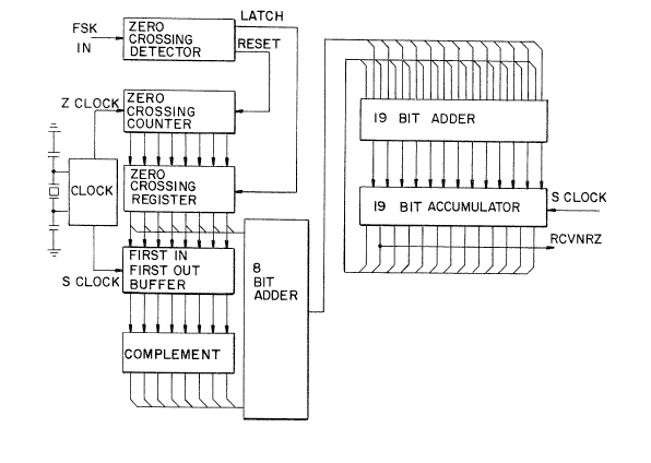
Fig. 2 illustrates the digital FSK receiver of the present invention. It
has been designed so as to use most of the circuitry in the FSK transmitter
shown in Fig. 1. In Fig. 2, intervals between zero crossings are converted to
numoers by counting the pulses of a clock, labelled ZCLOCK, in a counter. At
eacn zero crossing the count resulting from the previous interval is stored in
a register. On each pulse of clock SCLOCK the value of the
register is inserted in a 16 deep, 8 bit wide FIFO (first in
first out) buffer. An accumulator stores the sum of the values
in the FIFO (plus a fixed offset). RathPr than sum the 16 values
each time, the accumulator is kept current by subtracting the
oldest value in the FIFO from the new value being inserted and
adding the resultant to the accumulator.
If the received signal were a continuous zero (30.5 KHz), it
would have zero crossing intervals of 16.393 microseconds. A
continuous one (19 KHz) would have zero crossing intervals of
26.316 microseconds. With a ZCLOCK of 6 MHz these intervals
would yield counts of 98 and 158 respectively. Thus a continuous
0 input would give a value for the sum of the FIFO of 1568 and a
continuous 1 input would give a value of 2528. The mid-point is
2048, or 2**11th. As seen in Fig. 2, the baseband output is the
12th stage of the accumulator (a one in the 12th stage has a
value of 2**11th).
When the transmitted data changes from 1 to 0 (or 0 to 1)
there will be one zero crossing interval which will be between
the two extremes. This intermediate count contains information
which allows the receiver to determine where within the interval
the change occurred. It is imperative for minimum jitter
reception that this intermediate value be retained.
In the present embodiment, the SCLOCK is 250 KHz and,
because the 13 stage adder is relatively slow, it is not
practical to subtract the old value of the buffer between
7 3~. ' .
successive SCLOCK. Instead, an 8 bit adder calculates the
difference between the new and the old values of the FIFO and
this result is added to the accumulator of the SCLOCK rate. It
is important to notQ that the result to be added to the
accumulator may be positive or negative. A negative number from
the 8 bit adder is automatically expressed in two's complement
form and so adding it to the accumulator will give the correct
result.
CA~ N~
The receiver of the present invention has been simulate~ using several
BASIC programs. Calculations were performed to determine the spacings vf zero
crossings which would result from a p~rfect FSK transmitter being modulated
by an input data stream. Delays were investigated for one to zero transitions
and for zero to one transitions and the phase of the input data stream to the
FSK signal was varied over all the possible values in increments of 1
microsecond.
In the first program9 the delay in the change of the output relative to a
change in the input data stream from a one to a zero, was investigated. The
time t = O, was arbitrarily set to the last zero crossing before the input
data changed. The program was run a number of times for the input changing at
t = 1 microseconds, 2 microseconds, up to 26 microseconds. The llmit is 26
microseconds because, if it were any later than that, another zero crossing
would occur before the lnput change. Fig. 3 shows the distrlbution of the
delays (time of output change minus time of input change). The actual values
are given in Table 1, and the program is listed in Table 2.
Similarly, the delay due to a change from a zero to a one was
investigated. The distribution is shown in Fig. 4, the values are listed in
Table 3, and the program is given in Table 4.
When the programs were originally run, the distribution for both cases
was about +/- 3.5%, but the average delays were different. This would result
in a bias, causing ones and zeros not to have the same duration. The simplest
way to counteract this bias ls to offset the value stored in the accumulator,
i.e., Accumulator Value = Sum of FIFO + NcOR where NcOR is a positive or
negative integer.
A third program was run to demonstrate the circuit's response to a random
input. The plot of the accumulator value compared to the input waveform is
shown in Fig. 5.
~ ,:, . 7
C~L BNI-464
In Fig. 5, the solid line waveform is the data input to an FSK
transmitter. The ones and zeroes helow the waveform show the data to be
transmitted to a dlstant receiver. The dotted line waveform is the value in
the accumulator of the distant receiver. As can be seen ln Fig. 5, the dotted
llne waveform has a number of changes in slope which will be described in more
detail below.
The upper fla~ portions of the dotted line waveform indicate that the
FIF0 contains 16 values of 158. The lower flat portions of the dotted line
waveform indicate that the FIF0 contains 16 values of 98. The slopes whlch
connect the upper and lower portions are a functlon of when the change from a
one to a zero or a zero to a one has occurred. If the data transition occurs
at a zero crossing there will be a single slope. If the transition occurs
between zero crossings an intermediate count will be stored in the FIF0 and
three different slopes will occur as shown at slope A, which is a transition
between a received one and a received zero, in the dotted line waveform. An
enlargement of the slopes of A is shown in Fig. 5A.
Just prior to the first slope in A, a one is being received and 158 is
being shifted in an out of the FIF0. Slope 1 of A occurs because 158 is being
shifted out of the FIF0 but a value less than 158 (and greater than 98~
is being shifted in. Slope 2 occurs because 98 is being shifted into the FIF0
and 158 is being shifted out. Slope 3 occurs when the intermediate values are
shifted out of the FIF0 and 98 is being shifted in. When all of the
intermediate values are shifted out of the FIF0, the FIF0 is loaded with all
98s and the waveform is at the lower flat portion. To make it easier to
compare the two waveforms, they are shown in Fig. 6 with input delayed. In
both plots, the dotted line is set at the count 2048. The program is listed
in Table 5.
C~,~ sNI-464
A basic design for an all-digital FSK circuit has been disclosed.
Without any enhancements. it is likely that the design would satisfy all basic
requirements.
Fig. 7 shows the actual results achieved in a gate array chip ~1~ ~ w~L~i
according to the present invention. Fig. 7 illustrates the delay between the
transmitted signal CHl and the received signal CH2.
While a specific embodiment of the invention has been shown and descrlbed
in detail to illustrate the applicatlon of the principles of the lnvention, lt
will be understood that the lnventlon may be eMbodied otherwise without
departlng from such princlples.
C~ BNI-464
TABLE 1
U: U O O O (~
5 ! O O O U ()
]0: U U U O U
15: U U U U 0
2U: 0 0 0 0 0
25: 0 0 '0 0 U
~0: 0 0 0 0
35: 0 U 0 U U
'1 U ! U ~ O ~ ~ ~
'15:U O U O O
5U: 0 ~3 ~ U ~ t
55:111 15~ 26~ 2~U lGfi
fiU:~30 13 0 U
fi5:0 0 U 0 0
70: 0 U 0 U U
75:~) 0 ~) U
~U: U U U U U
BS: O O O O O
90:(~ O O O u
95: 0 0 o o U
TABLE 3
0: 0 0 0 0 0
5: 0 0 0 () U
10: 0 U , O U (~
15: 0 0 0 U ()
20:0~ U 0 0 U
25:~ 0 0 0 0 U
30:,/ U U ~ ~ U
35: U ~ U o
~tO~U U O U O
~5: U 0 0 0 0
~ ~ 0 17. G9
55:129 liU 162 lU'i ~G
6U: ~ U U U
65: 0 0 . 0 U U
70: 0 0 0 0 0
75: 0 0 0 0 0
OU: O U O O U
05: 0 0 0 0 0
9U: O U O O U
95: U O O O
2r3~J~ 7
w~SE l~NI-464
TABLE 2
t~EM ~ I)ISTlV -~ J *
Ol'Etl "FIG~.'1'13L" FOII OUTPU'r AS tll
'I'lll~ = ~o,~t3
~O IllPU'r "OFFSET" :OFFSE'r
TICK = 4
ZTICI( = I/G
DIM l~'1'13L( loo~
uo zr~rn~uJ = 10()0/Gl
Zr'r,Q(l) = 1000/3t3
100 7,CIIT(O~ = Ill'r(ZE'En~O~/ZTICK) ~ OFFSE'r
11(1 ZCN~r(l) = II~T~ZPEr~(l)/ZTICK) + OFFSE'r
120 FOQ J = O l'O t10
1:~0 L~l r = O
140 FOII I = 0 'l'O INT(ZPEn(l) )
150 ~TM E ~ J ~ ~10) '~ TI C K
160 zct~r- zc~r(u)
17() l)~ r + 1
1130 I\CC = lG~ZCNT(l)
190 7.Ill'r '~ r + ( 1 - L~I~r/Zpr~ zr~
2()0 A'l'ME = A'1'11E + 'l'ICK
210 IF (ATME < ZIIIT) 'l'llEII GOTO 200
220 ZCNT = Il~'r(~IIIT/Z'rICI<) + OFFSET
230 ACC = ACC - ZCIIT ~ 1) + ZCS~T
240 ~ ME = ATME ~- TICIC
250 IF (~\CC c=~ Tllll) l'llEII GOTO 310
2G0 IF (~\'l'ME ~= (7~ T + ZP~n(O))) GOTO 230
27 U ZCIiT = ZCNT (0)
2t30 ACC -- ACC -Z~CN'r(l) + ZCNT
29() A'l'M~ = A'l'ME 1- TICK
300 IF (ACC ~ '1'lll~) GO'l'O 2MO
310 I)ELAY = IIIT(A'l'Mr. - 1)1'1' ~ .5)
320 l)'l' BL(I)E LA Y ) ~ r B L ( DE L ~Y ) +
330 I'IEXT I
3~'10 ~EX'r J
350 CLS
360 5CllEE11 2, O
37U /I<EY OFF
3130' ' FOI~ I -- O '1'0 99
390 LINE ~51~I,150) - (5~I,15U - l)TDL(I)/2)
~100 LIlIE ~5~I + 1,150 - (5J~I + 1,150 -- D'l'llL(I)/2)
~l10 LIIIE 5~I + 2,150 - (51~I + 2,150 - l)'l'DL(I)/2~
~120 J,II~E ~5~I + 3,150) - (5~I ~ 3,150 - DTBL(I)/2)
llr,x~r -
o For~ I = 1 l'O 10
~150 ~SET(50*I - 5,153)
/I G0 IIEX'l' I
~170 LOCATE 22
~lUO sror~
~90 SOIIEEN 0,0,0
5 () () For~ I = 1) l'O 19
510 Vl\ll = 5~I.
520 1'11I1l'r ~ " ,VA~J
53 O Foll J ~ O TO ~1
5~10 VA~l = 5~I ~ J
550 I' II I lI'r ~ l , l)'r B L ( VA
56() I'~r'X'l' J
570 ~ J r R l, " "
5UO !IEX'r I
C~;,E BN 1-~ 6
'I'ABLE 4
~ E: t l ~ V I S '1' ~ 1 * ~ ~ ~ *
C1rl~lJ IIFI(/7.TDLI~ FOn OU'l'PUT ~S ~1
3 0 '1' ~ I ~l = 2 ~ 3
~1() IllE'UT"OFFSET'I;OFFSE'r
5 0 '1' r C K = ~t
~,TICK = 1/6
7 0 L~M L?~l~ lL ( 10U )
110 ZPE[~O, ~ 1000/61
so zr~n 1 ~ 1000/38
~ oo zc~ r ~ o, -- Ill'r ~ ZE~ ( o ~ /ZTICK) ~- O~FSEl'
1]0 ZC~Tt1, = IliT~ZPER(1)/ZTICK) ~ OFFSE'r
.1ZO ~on ~ - o ~l~O ~(~
130 L)IT = U
() FO~ I = O TO I~T(ZPER(O) )
150 i~'l'l1E ~ ~1 -J/~lO) ~r'l' 1 CK
160 zcllr -- ZCIJ~(o) + oFFsEr
170 DI'r = L~I'r + 1
luo l\CC= l6~zc~r(0)
190 zlll'r = l~l~r ~ l3I'l'/ZPt~ (O) ) J~%1'l~l~(1)
:~ 0 0 ~'rM I~ E + 'I' l C K
210 IF (~TI~E < ZI~l'r) 'I'IIEII GOTO 200
220 ZCI~T = II~T(ZII~'r/Z'rICI~) + OFESE'r
'230 I~CC = I\CC ~ Z C~'r(O) + ZCN'r
2 ~10 I~'l'tlE = I~TME + TICK
250 IF ~/~CC >= Tllll) 'rl~ 3 GOTO 310
2GO ~:F (~ lL ~~ (Zlll'r -1- ZPE1~1) ) ) GO'l'O 230
27U ZCII'l' = ZCI~'r(1J ~ OFFSE'l'
~no ~cc - ACC ~ ZC~IT~O) + zct~'r
2 90 - I\'lME -- ~'1ME ~ ~rICK
300 lF (~CC ~ Ttlll) GO'I'O Z50
3 10 U E LJI~ Y ~ I I l'r ( /~'L'11 E ~ L) 1'1' ~ . 5 )
~ 2 0 U'l'UL ( DEL~Y ) = L~'l'B~ ( UEl~Y ) +
] 3 0 IIEX'l' I
3/10 ~IEXT J
~50 CLS
3 60 SCnEE~I 2, U
370 ~ KEY OFF
] U 0~ FOII I = O l'O Y 9
390 LlllE ~5~ ISO] ~ (5t'1,150 ~ D'1'13L(IJ/2)
~100 LIli~ 5~I + 1,150) (5J~ 150 - 1~'rDL~(I)/2)
~1 10 LII~F i5~ 1- 2 ~ 150~ ~ (S~'l + Z ~ 150 ~ I)'l'DL(I) /2)
~120 LII~ 5~ 3~150) ~ (5~I ~ 3~150 -- L~'l'L~L(I)/2)
/1 1o llEX'l' r
l~o Fon 1 = 1 TO 10
~150 PS~'r ( 50t~I ~ 5 ~153 J
~EX'r r
~170 LOC1~'rE 22
~UO S'l'OP
~190 SCI~EEI~ o,b,u
500 FOI~ I = O TU 19
5 10 V~ = 5 ~l
520 P~ r Nl, v~
5 3 0 1;'0l~ J = O '1'0
5/10 Vl\1~1 = 5
5 5 0 ~ r ~ 1, D'l' B I~ ( V~
5~0 I~X'l' J
575) IlEX'
r)no CLUSL'
~3
,y~',jF ~ ~
CA:~I. BNI-~64
TABLE 5
DIU~TE -- 9.600001
TICK = 4
ZTICK = 1/6
IU Pll = 12
SMPL5 = 100
DlM ZT~3L'SMPLS)
DIM L)'1'13L 6()0)
~10 DIM ATBL'SMPLS)
DIM ACCTqL(600)
1()0 ~CC = 16*9~1
110 ZE'En 'O I = 16.393
12U '~ .11 1, ' 2fi .316
130 ZCII'I''0 ~ Ii~'r(ZPE:II(0~/Z'rICK)
140 Z,CIIT,l~ T(ZPE~(l)/Z'rIC~C)
150 L)VA[,- = 27
16U l)Vl\L = DVALI
170 DrEn = 10UU/13n/~TE
1)30 ~3'1'11E = 13PER
190 1) = O
200 ~IXL) = 1
210 Eon I = 1 TO SMPL5
220 D'1'8L(I~ = A'l't1E
230 IF (ZPEn(l)) > 13TME) TIIEI~ GOTO 240 ELSE GOTO 33U
2 ~ 0 n = 13~rl~E~ z ~Er~
250 ZIliT = R~ZPEn(D) + (1 - n) ~ZPER~NXL))
260 D = NXD
Z70 IIXDl = (DVAL l\ND 64)/64
2130 11XD2 = (DVAL l\IID 32)/32
290 IIXD = IIXI)l XO~ NXV2
300, l)Vi\L = (l)Vl~L~2 + tlXD) MOD 128
310 ' 13'1'1~E = 13TI~E + DPEn
320 GOTO 340
330 ZIll'r = ZE'Ell(L))
340/ A'l'l~E = I~TME + ZIN'r
350 ATnlJ(I) = ATME
360 13'1'11E = 13TI~E -- ZIll'r
370 Z'l'DL(I) = IN'r~ZIN'r/ZTICK)
330 %T11E = ZIN'r
390 I~F,XT I
4()0 FIII = 16
'110 L)II~ FIFO(FIIJ)
420 F()R I = O To 15
430 I:IFO(I) = 9i3
440 IIEXT I
CASE ~NI-46
TABLE 5 (CONTINUED)
~50 ~'L'~(o) ~ ~
~60 Z~l'DL(o) ~ 16.913
~70 TPTR = 1
a o TME = O
~90 TPT~ = l
500
510 TP'l'~ = TP'rn + 1
520 ~lV~L = Z'r~l,('rr'rn)
530 llSMPL'-~ - INT~ATUL(SMPLS)/'rICK)
5~0 FOR I = 1 ~'O NSMPLS
550 TME = I'ME + TICK
560 ~F ~TME <- ~T~L(TPTQ)) TIIEN GOTO 580
510 TP'rR = TPTR + 1
530 ~FIFO = ZT~L('rPTll - 1)
590 ~CC = ~CC - FIFO(FPT~) + ~EIFO
600 ~CCT~ CC
610 FIFO(FP'I'R) = S~FIFO
620 FP'l'R = (FPTn ~- 1) MOD 16
630 IlEx~r I
6~0 ~V~L -- UV~LI
650 l) = o
660 IIXI) = l
670 8'L'ME = 1U00/~ TE
600 Fon I = 1 TO ~ISMPLS
690 l)'rl3L(I) = L)
700 i3'1'ME = ~TME - TI CK
710 IE (~'rt1E > O) l'IIEII G01'0 780
720 13'1'I~E ~ B'1'11E ~ lOOO~DI~'rE
730 D - NXD
740 NXDl ~ (UV~ ~IID 6~)~6~
750 1~X~2 = (DVAL ~ND 32)/32
760 NXD = NXDl XOII ~IX1~7.
770 W~L = ~2~DV~L ~ NXD) l~OD 128
780 ~lIF.X'r I
790 ~ CLS
800 SCl7EEII 2, O
810 ~'Y~EY OFF
820 PSET(0,98)
û30 FOI~ I = lG ~0 NSMPLS
8~0 Y = IN'r(~CC'r~L(I)~l6)
~50 rs~r (I,Y)
860 PSET~I,113 ~ 30~ L(I - Pll)j
86l IF (UT~ Pll -1) Y D'rSL(I - Pll)) 'rllE~I GO'l'O 870
t36 2 FO~ J = 0 ~'O 80
363 PSE'r5I,113 + J)
36~ llEX1' J
370 IF ((I ~D 6) = O) TIIEN PSE'r(I,l28)
~o lI~X'r I
~90 1~C~T~ 22, ~0
goo V - ~III'I' ( lO~UI~'rE)
9 10 V = V~ 10
920 PRIN'r" RESPONSE ~OR I'5VIII ~ILO~UD"