Note: Descriptions are shown in the official language in which they were submitted.
20773 59 ~
TITLE OF THE INVENTION
X-RAY MASK AND SEMICONDUCTOR DEVICE MANUFACTURING METHOD
USING THE SAME
BACKGROUND OF THE INVENTION
Field of the Invention
The present invention relates to an X-ray mask used
in a semiconductor exposure device using an X-ray
source, a method of manufacturing the X-ray mask and a
semiconductor device manufacturing method using the X-
ray mask.
Description of the Related Art
An example of generally known X-ray masks used in
X-ray exposure devices is described below.
As shown in Fig. 10, an X-ray mask substrate 50 is
joined to a mask frame 54. The X-ray mask subst~ate is
produced by depositing an inorganic film 52 of SiN or
the like on the surface of a silicon substrate 51,
removing a portion corresponding to a permeable film
portion 52a by dry etching, and removing a portion of
the silicon substrate 51 which corresponds to the
permeable film portion 52a by wet etching. A pattern
55 made of an X-ray absorber such as Ta, Au or the like
is provided on the permeable film portion 52a in
`- 207735~ -2-
correspondence with a predetermined shape to be
transferred to a wafer (not shown).
When exposure is performed by an exposure device to
`which the X-mask is fitted, the surface of the X-mask in
which the pattern is formed is opposed to a wafer at a
distance of about 30 ~m. In this state, a portion of
the wafer is exposed to light. When another portion of
the wafer is then to be exposed to light, the distance
between the X-ray mask and the wafer is increased to
about 200 ~m, and the X-ray mask is then moved to a
position corresponding to the other portion. The
distance between the X-ray mask and the wafer is then
returned to about 30 ~m, and the other portion is
exposed.
The step-and-repeat operation is successively
repeated to expose the wafer.
However, during exposure using the above ~-
conventional X-ray mask, when the X-ray mask once
separated from the wafer is brought back close to it, if
the X-ray mask is rapidly moved, the gas present in the
gap between the X-ray mask and the wafer cannot easily
escape from the gap and is thus compressed as the X-ray
mask is brought close to the wafer. The pressure of
the gas between the X-ray mask and the wafer is thus
increased in correspondence with the speed of movement
21~77359
~ . . .
of the X-ray mask toward the wafer. This increase in
the pressure causes a danger of breaking or damaging the
permeable film portion serving as a permeable support
film. There is also the problem that if the speed of
movement of the X-ray mask toward the wafer is decreased
for preventing the breakage of the permeable film
portion, the productivity of the exposure device is
decreased.
SUMMARY OF THE INVENTION
The present invention has been achieved for solving
the above problems. It is a first object of the
present invention to provide an X-ray mask and a method
of producing the X-ray mask which permits an increase in
the speed of movement thereof without breaking or
damaging a permeable film portion and which increases
the productivity of the exposure process.
It is a second object of the present invention to
provide a semiconductor device manufacturing method with
high productivity using the X-ray mask and a
semiconductor device manufactured by the method.
Other objects of the present invention will be made
apparent from the detailed description of preferred
embodiments below.
2077359
BRIEF DESCRIPTION OF THE DRAWINGS
Fig. 1 is a partially broken-out perspective view
of an X-ray mask in accordance with a first embodiment
of the present invention;
Fig. 2 is a drawing showing a process of
manufacturing the X-ray mask shown in Fig. 1, in which
Fig. 2(A) is a drawing showing a step of depositing an
inorganic film on a silicon substrate, Fig. 2(B) is a
drawing showing a step of removing portions of the
inorganic film which correspond to a permeable film
portion and through holes, Fig. 2(C) is a drawing
showing a step of removing portions of the silicon
substrate from which the inorganic film is removed, Fig.
2(D) is a drawing showing a step of removing portions of
the inorganic film which correspond to the through
holes, and Fig. 2(E) is a drawing showing a step of
joining a mask frame to the X-ray mask substrate formed
through the steps shown in Figs. 2(A) to 2(D);
Fig. 3 is a sectional view of a principal portion
showing the flow of gas when the X-ray mask shown in
Fig. 1 is attached to an exposure device and is brought
close to a wafer;
Fig. 4 is a partially broken-out perspective view
of an X-ray mask in accordance with a second embodiment
of the present invention;
2077359
Fig. 5 shows a process of manufacturing the X-ray
mask shown in Fig. 4 and is a sectional view of the X-
ray mask taken along a plane passing through the center
of the X-ray mask and parallel to one side thereof, in
which Fig. 5(A) is a drawing showing a step of
depositing an inorganic film on a silicon substrate,
Fig. 5(B) is a drawing showing a step of removing a
portion of the inorganic film which corresponds to a
permeable film portion and the circumference thereof,
0 Fig. 5(C) is a drawing showing a step of removing the
portion of the silicon substrate from which the
inorganic film is removed, Fig. 5(D) is a drawing
showing a step of removing the circumference of the
permeable film portion, and Fig. 5(E) is a drawing
showing a step of joining a mask frame to the X-ray mask
substrate manufactured through the steps shown in Figs.
5(A) to 5(D);
Fig. 6 is a sectional view of a principal portion
showing the flow of gas when the X-ray mask shown in
Fig. 4 is fitted to an exposure device and is brought
close to a wafer;
Fig. 7 is a drawing showing the arrangement of an
X-ray exposure device;
Fig. 8 is a drawing showing a semiconductor device
manufacture flow;
2077359
. .
Fig. 9 is a drawing showing a wafer process flow;
and
Fig. 10 is a sectional view of a conventional X-ray
mask.
DETAILED DESCRIPTION OF THE PREFERRED EMBODIMENTS
Embodiments of the present invention are described
below with reference to the drawings.
An X-ray mask in accordance with a first embodiment
of the present invention is described below with
reference to Fig. 1.
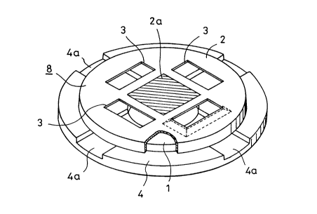
The X-ray mask of this embodiment comprises a disk-
like mask frame 4 having an opening concentrically
formed at the center thereof, and an X-ray mask
substrate 8 joined to the surface of the mask frame 4
and having a diameter greater than the diameter of the
opening of the mask frame 4. ~~
Four grooves 4a are radially formed at equal
intervals in the plane of the mask frame 4 which is
joined to the X-ray mask substrate 8, so that the
grooves 4a connect the internal perlphery of the mask
frame 4 with the external periphery thereof and
communicate with the through holes 3 below.
On the other hand, the X-ray mask substrate 8
comprises a silicon substrate 1 having an inorganic film
-7-
2077359
~ ,, .
2 of SiN or the like deposited on the surface thereof.
The central portion of the silicon substrate 1 is
rectangularly removed leaving the inorganic film 2 on
the side opposite to the junction plane of the mask
frame 4. A permeable film portion 2a (the shadowe'd
portion shown in Fig. 1) comprising the inorganic film 2
on the side opposite to the junction plane is formed in
the central portion of the silicon substrate 1. A
pattern 5 (refer to Fig. 2(E)) made of an X-ray absorber
such as Ta, Au or the like is provided on the permeable
film portion 2a in correspondence with a predetermined
shape to be transferred to a wafer.
Four rectangular through holes 3 each serving as a
gas passage are formed around the permeable film portion
2a of the silicon substrate 1 so as to respectively
correspond to the grooves 4a formed in the mask frame 4.
The process of manufacturing the X-ray mask of this
embodiment is described below with reference to Fig. 2.
As shown in Fig. 2(A), the inorganic film 2 of SiN
or the like is first deposited on the surface of the
silicon substrate 1.
A dry etching resist is then coated on the
inorganic film 2, and portions of the resist which
correspond to the permeable film portion 2a and the
through holes 3 are removed by exposure to form a dry
207735~
. . .
etching mask. As shown in Fig. 2(B), portions on the
upper side of the inorganic film 2 which correspond to
the permeable film portion 2a and the through holes 3
` are removed by dry etching.
S As shown in Fig. 2(C), portions of the silicon'
substrate 1 from which the inorganic film 2 is removed
are removed by wet etching to form the permeable film
portion 2a.
As shown in Fig. 2(D), the remaining portions of
the inorganic film 2 which respectively correspond to
the through holes 3 are removed to form the through
holes 3. In this way, the X-ray mask substrate 8 is
formed. The portions of the inorganic film 2 which are
desired to be removed may be removed by wet etching or
mechanical means using a cutter or the like.
As shown in Fig. 2(E), the pattern 5 made of an X-
ray absorber such as Ta, Au or the like is then formed
on the lower side of the inorganic film 2 shown in the
drawing on the permeable film portion 2, and the through
holes 3 are respectively aligned with the grooves 4a.
The X-ray mask substrate 8 is joined to the mask frame 4
in parallel with each other by an adhesive.
When exposure is performed using the X-ray mask of
this embodiment, as shown in Fig. 3, the X-ray mask 10
vertically held by a mask chuck 6 is moved to the left
2077359
of the drawing so as to be brought close to a wafer 7.
At this time, the He gas present between the X-ray mask
10 and the wafer 7 passes through the through holes 3
and the grooves 4a and flows to the side of the X-ray
mask 10 and to the mask chuck 6. Thus the pressure of
the He gas present between the X-ray mask and the wafer
7 is not increased, and if the X-ray mask 10 is rapidly
brought close to the wafer 7, there is no danger of
breaking the permeable film portion 2a serving as a
0 permeable support film.
In addition, the formation of the through holes 3
and the grooves 4a in the X-ray mask substrate 8 and the
mask frame 4, respectively, decreases the weight of the
X-ray mask 10 and thus decreases the load on a mask
conveyance system comprising a mask hand or the like in
an exposure device. As a result, the mask conveyance
system can be decreased in size and weight.
Although, in this embodiment, four through holes 3
and four grooves 4a are formed, the number of through
holes or grooves is not limited to 4, and can be changed
according to demand. In addition, the grooves 4a need
not be provided, and through holes may be formed in the
mask frame 4 in place of the grooves 4a. However, when
through holes are formed in the mask frame 4, X-ray
- 1 0 -
2077359
. . .
radiation must be shielded by an aperture so as to
prevent the X-rays from leaking from the through holes.
An X-ray mask in accordance with a second
embodiment of the present invention is described below
with reference to Fig. 4.
The X-ray mask of this embodiment comprises a disk-
like mask frame 14 having an opening concentrically
formed in the central portion thereof, and a square
plate X-ray mask substrate 18 joined to the surfacé of
the mask frame 14.
The X-ray mask substrate 18 comprises a silicon
substrate 11 having an inorganic film 12 formed on the
surface thereof. The X-ray mask substrate 18 also has
a permeable film portion 12a (the shadowed portion shown
in the drawing) formed in the central portion thereof.
The length of the diagonal of the X-ray mask substrate
18 is greater than the diameter of the opening of~the
mask frame 14, and the length of one side of the X-ray
mask substrate 18 is smaller than the diameter of the
opening of the mask frame 14. In the state where the
X-ray mask 18 is joined to the mask frame 14, the
opening of the mask frame 14 is thus not closed by the
X-ray mask substrate 18, thereby forming gaps 13 serving
as gas passages between the opening and the X-ray mask
18.
- 2077359
.
Since the permeable film portion 12a may be
configured in the same way as that in the first
embodiment, it is not described below.
The process of manufacturing the X-ray mask of this
embodiment is described below with reference to Fig'. 5.
As shown in Fig. 5(A), the inorganic film 12 of SiN
or the like is deposited on the surface of the silicon
substrate 11.
A dry etching resist is then coated on the
inorganic film 12, and portions of the resist
corresponding to the permeable film portion and the
circumference thereof are removed by exposure to form a
dry etching mask. As shown in Fig. 5(B), portions of
the inorganic film 12 on the upper side thereof, which
correspond to the permeable film portion and the
circumference thereof, are removed by dry etching.
As shown in Fig. 5(C), portions of the silicon
substrate 11 from which the inorganic film 12 is removed
are removed by wet etching to form the permeable film
portion 12a.
As shown in Fig. 5(D), the portions of the
inorganic film 12 which remain in the circumference are
removed to form the X-ray mask substrate 11. A portion
of the inorganic film 12 which is desired to be removed
207735~
. .,
may be removed by wet etching or mechanical means using
a cutter or the like.
As shown in Fig. 5(E), a pattern 15 made of an X-
ray absorber such as Ta, Au or the like is formed on the
lower side of the inorganic film 12 on the permeable
film portion 12a shown in the drawing, and the X-ray
mask substrate 11 is joined to the mask frame 14 in
parallel with each other by an adhesive.
During exposure using the X-ray mask of this
embodiment, when the X-ray mask 20 vertically held by a
mask chuck 16 is moved to the left of the drawing so as
to be brought close to a wafer 17, as shown in Fig. 6,
the He gas present between the X-ray mask 20 and the
wafer 17 passes through each of the gaps 13 and flows to
the mask chuck 16, as shown by arrows in the drawing.
Thus the pressure of the He gas present between the X-
- ray mask 20 and the wafer 17 is not increased, and~there
is no danger of breaking the permeable film portion 12a
serving as a permeable support film even if the X-ray
mask 20 is rapidly brought close to the wafer 17.
In addition, since the X-ray mask substrate 18 has
a necessary minimum configuration including the
permeable film portion 12a, it is possible to decrease
the weight of the X-ray mask 20 and decrease the load on
a mask conveyance system comprising a mask hand or the
2077359
., .
like in an exposure device. The mask conveyance system
can be consequently decreased in size and weight.
Further, since the area of the portion facing the
wafer is decreased by decreasing the size of the X-ray
mask substrate 18, the flatness of the plane of the X-
ray mask 20 which faces the wafer 17 can be improved.
Although, in the X-ray mask of the above
embodiment, the X-ray mask substrate 18 and the opening
of the mask frame 14 have a rectangular shape and a
circular shape, respectively, both shapes may be
interchanged. Any desired shape can be selected unless
the opening is closed by the X-ray mask substrate 18
when the X-ray mask substrate 18 is joined to the mask
frame 14.
In the X-ray mask of each of the embodiments, the
X-ray mask substrate has gas passages provided in the
perimeter of the permeable film portion so as to connect
the one side of the substrate with the other side
thereof. This causes the gas present between the X-ray
mask and the wafer to pass through the gas passages and
flow to the other side of the X-ray mask substrate when
the X-ray mask is moved toward the wafer during
exposure, without increasing the pressure between the X-
ray mask and the wafer. Since there is thus no danger
of breaking the permeable film portion, it is possible
-14-
207735~
to increase the speed of movement of the X-ray mask and
improve the productivity of the exposure device. This
is significantly effective for step-and-repeat type
exposure. In addition, since the weight of the X-ray
S mask is decreased by providing the gas passages in the
X-ray mask substrate, the mask conveyance system of the
exposure device can be decreased in size and weight.
In addition, when the grooves are radially formed
in the surface of the mask frame which is joined to the
X-ray mask substrate so as to communicate with the gas
passages so that when the X-ray mask is moved toward the
wafer, the gas present between the X-ray mask and the
wafer can be effectively made to escape from the spaces
between the X-ray mask and the wafer.
Further, since gaps are produced between the
opening of the mask frame and the X-ray mask substrate,
when the X-ray mask is moved toward the wafer during
exposure, the gas present between the X-ray mask and the
wafer passes through the gaps and flows to the other
side of the X-ray mask substrate, without increasing the
pressure between the X-ray mask and the wafer. Since
there is thus no danger of breaking the permeable film
portion, it is possible to increase the speed of
movement of the X-ray mask and improve the productivity
of the exposure device. Since the X-ray mask substrate
2077359
.,
has a necessary minimum structure outside of the
circumference of the permeable film portion, the X-ray
mask substrate can be decreased in weight, and the mask
conveyance system of the exposure device can be
decreased in size and weight. The smallness of the
- area of the surface of the X-ray mask substrate which
faces the wafer during exposure permits improvement in
the flatness of the surface.
In the method of manufacturing the X-ray mask
substrate, the gas passages are formed by removing the
inorganic film remaining in the portions on the other
side of the silicon substrate, which correspond to the
gas passages, in the same process as that for forming
the permeable film portion. In this way, the gas
passages can easily be formed by adding a simple step of
removing the inorganic film in portions corresponding to
the gas passages to a conventional method of ~~
manufacturing an X-ray mask substrate.
A description will now be made of an embodiment of
an X-ray exposure device for manufacturing a
semiconductor device using the aforèmentioned X-ray
mask. Fig. 7 is a drawing showing the configuration of
the X-ray exposure device of this embodiment. In the
drawing, the sheet beam-like synchrotron radiation
emitted from a radiation source 20 such as an SOR ring
-16-
-- 2077359
. . .
or the like is enlarged and reflected by a fixed convex
mirror 22 in the direction (y direction) vertical to the
radiation orbital plane so that the whole exposure
region Lo can be irradiated. X-rays are extracted from
the synchrotron radiation 21 reflected and enlarged'by
the convex mirror 22, and exposure within the
irradiation region is adjusted by a shutter 23 for
controlling exposure. The X-rays passing through the
shutter 23 are led to an X-ray mask 24 held by a mask
chuck. The X-ray mask 24 has the same structure as
that of the above-described embodiments. The circuit
pattern formed on the X-ray permeable film portion of
the X-ray mask 23 is projected on a silicon wafer 25
coated with a resist by step-and-repeat type exposure.
The X-ray exposure device of this embodiment
permits an increase in the speed of movement of the X-
ray mask toward the wafer and thus has the effect~of
increasing the productivity. This effect is remarkable
in step-and-repeat type exposure in which the operation
of bringing the X-ray mask close to the wafer is
repeated several times.
A description will now be made of an embodiment of
a semiconductor device manufacturing method employing
the above exposure device. Fig. 8 shows a manufacture
flow for semiconductor devices (a semiconductor chip
207735~
, . .
such as IC, LSI or the like, a liquid crystal panel, CCD
or the like). In Step 1 (circuit design), the circuit
of a semiconductor device is designed. In Step 2 (mask
manufacture), a mask on which the designed circuit
pattern is formed is manufactured. In Step 3 (wafer
manufacture), a wafer is manufactured using a material
such as silicon or the like. In Step 4 (wafer process,
which is called pre-process), an actual circuit is
formed on the wafer by lithography using the prepared
mask and wafer. In Step 5 (assembly, called post-
process), a semiconductor chip is formed by using the
wafer produced in Step 4. The post-process comprising
the assembly step (dicing, bonding), the packaging step
(chip sealing) and the like. In Step 6 (inspection),
tests of the semiconductor device formed in Step 5, such
as the operation confirmation test, the durability test
and the like, are carried out. The semiconductor~
devices completed through the above steps are shipped
(Step 7).
Fig. 9 shows the detailed flow of the above wafer
process. In Step 11 (oxidation), the surface of the
wafer is oxidized. Step 12 (CVD), an insulating film
is formed on the surface of the wafer. In Step 13
(electrode formation), electrodes are formed on the
wafer by vapor deposition. In Step 14 (ion
-18-
2077359
implantation), ions are implanted in the wafer. Step
15 (resist process), a sensitizer is coated on the
wafer. In Step 16 (exposure), the circuit patter on
the mask is transferred to the wafer by exposure using
S the aforementioned exposure device. In Step 17
(development), the wafer exposed is subjected to
development. In Step 18 (etching), portions other than
the developed resist image are etched. in Step 19
(resist separation), after etching, the unnecessary
resist is removed. These steps are repeated to form a
multiple circuit pattern on the wafer.
The above description has been given on preferred
embodiments of the present invention, but it will be
apparent to those of ordinary skill in the art that many
changes and variations are possible without departing
from the scope of the present invention, which is to be
determined by reference to the appended claims.