Note: Descriptions are shown in the official language in which they were submitted.
2077499
-
PATTERN STRUCTURE OF A PRINTED CIRCUIT BOARD
The present invention relates to the pattern structure of a printed
circuit board for mounting various kinds of electronic chip parts.
It has been customary to solder electronic chip parts to patterns
provided on a printed circuit board and implemented by, for example, copper
5 foil. In the SMT (Surface Mounting Technology) art, the above-mentioned
patterns are referred to as pads. In many cases, the pads are provided with a
rectangular shape, although the shape depends on the configuration of the
portions of the chip parts to be soldered. The pads located in a circuit-
connecting portion are often implemented as narrow patterns, while the pads
10 located in a ground-circuit portion are often implemented as a broad continuous
pattern, i.e. a solid pattern. Generally, a printed circuit board is provided with
a solder-resist coating on the surface thereof to prevent solder from depositing
in unexpected portions, or from bridging. In the circuit-connecting portion, the
pad is spaced apart from the solder-resist coating by a gap. In the ground-
15 circuit portion, the pad is formed by part of a solder-resist coating provided on
a solid ground pattern for grounding purposes.
The problem with the above-described conventional pattern
structure is that the pad in the circuit-connecting portion and the pad in the
ground-circuit portion are often different in size or area from each other. When
20 a chip part is soldered to such pads by, for example, a reflow process, the
temperature elevation rate differs from one pad to the other pad since the
pattern area, i.e. the area of copper foil, greatly differs. The difference in
'~C
A~-
.
2077~99
temperature elevation rate results in a difference in the melting time of solder
and, therefore, a difference in surface tension. This increases the probability
of a so-called tombstone phenomenon wherein the chip stands uneven.
Furthermore, since the two pads are different in area from each other and since
5 the amount of solder is fixed, the spread of solder, and therefore the
configuration of the resulting fillet, differs from one pad to the other pad, making
it difficult to perform a quality check.
It is therefore an object of the present invention to provide a
pattern structure of a printed circuit board adaptive to the miniaturization of chip
10 parts, i.e. miniature, dense packaging.
It is another object of the present invention to provide a pattern
structure of a printed circuit board which noticeably reduces the tombstone
phenomenon by substantially equalizing the temperature elevation rate in the
event of reflow.
It is another object of the present invention to provide a pattern
structure of a printed circuit board which facilitates quality checks by forming
fillets of identical shape.
A pattern structure of a printed circuit board for a surface-mounting
device of the present invention comprises a first pad provided in a circuit-
20 connecting portion of the printed circuit board, a second pad provided in a solid-
ground-pattern portion of the printed circuit board, and a cut formed in the solid-
ground-pattern portion, whereby the first pad and the second pad have
substantially the same area as each other.
L ~ ~
2077499
The above and other objects, features and advantages of the
present invention will become more apparent from the following detailed
description taken with the accompanying drawings, in which:
Figure 1 is a perspective view of a conventional pattern structure
5 of a printed circuit board;
Figure 2 is a plan view of the pattern structure shown in Figure 1;
Figure 3 is a section along line lll-lll of Figure 2;
Figure 4 is a perspective view of a pattern structure of a printed
circuit board embodying the present invention; and
Figure 5 is a plan view of the structure shown in Figure 4.
Referring to Figures 1 to 3, a conventional pattern structure of a
printed circuit board is shown. As shown, a printed circuit board, generally
designated 10, has a substrate 12 on which a solder-resist coating 14 is
provided. In a circuit-connecting portion C forming part of the printed circuit
board 10, a pad 16 is located and provided with a square shape, as indicated
by hatching in the figures. The pad 16 is spaced apart from the solder-resist
coating 14 by a gap 18 of between 0.1 millimeters and 0.2 millimeters,
depending upon positional deviations. In a ground-circuit portion E, forming
another part of the printed circuit board 10, a broad continuous, or solid, ground
pattern 20 is provided on the substrate 12. Specifically, a rectangular pad 22
located in the ground-circuit portion E, as indicated by hatching, is constituted
by part of a solder-resist coating provided on the ground pattern 20.
As shown in Figures 1 and 2, the pads 16 and 22 are different in
size from each other, i.e. the pad 16 is smaller than the pad 22 by an area
A~
2077~99
corresponding to the gap 18. Therefore, when an electronic chip part 24 is
soldered to the pads 16 and 22, the previously-stated tombstone phenomenon
occurs. Further, as shown in Figure 3, fillets 26 and 28 surrounding the chip
part 24 are different in shape from each other, resulting in troublesome quality
5 checks.
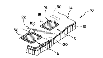
A reference will be made to Figures 4 and 5 for describing a
pattern structure of a printed circuit board embodying the present invention and
free from the above-described problems. In the figures, the same or similar
constituents to the constituents of the conventional structure are designated by
10 the same reference numerals, and to avoid redundancy will not be described.
In Figures 4 and 5, the reference numeral 30 designates a circuit pattern. In the
illustrative embodiment, a solid ground pattern 20 is partly removed to form cuts
32 around a pad 22 located in a ground-circuit portion E. As a result, gaps 18a
corresponding to a gap 18 which surrounds a pad 16 is formed around the pad
22. Hence, the pads 16 and 22 have substantially the same size or area as
each other. The pad 22 is connected to copper foil which forms the ground
pattern 20 surrounding the recesses 32.
In summary, the embodiment forms the cuts 32 in the ground
pattern 20 to thereby provide the pads 16 and 22 with substantially the same
20 area, and connects the copper foil surrounding the recesses 32 and the pad 22.
In this configuration, the pads 16 and 22 are heated at substantially the same
rate during reflow, noticeably reducing the tombstone phenomenon. In addition,
fillets to be formed around the pads 16 and 22 will have the same shape since
r~ ~
2077499
the pads 16 and 22 have substantially the same area, thereby facilitating quality
checks.
Various modifications will become possible for those skilled in the
art after receiving the teachings of the present disclosure, without departing from
5 the scope thereof.
r ~ ,~.