Note: Descriptions are shown in the official language in which they were submitted.
2077522
1 TITLE OF THE INVENTION
BATTERY FEED CIRCUIT FOR SUPPLYING FEED
CURRENT TO TELEPHONE SET
BACKGROUND OF THE INVENTION
(1) Field of the invention
The present invention generally relates to a
battery feed circuit, and more particularly to a battery
feed circuit for supplying a feed current to a telephone
set via a subscriber line.
(2) Description of related art
A battery feed circuit supplies a feed current
to a telephone set via a 2-wire telecommunication line
(a subscriber line). In a conventional battery feed
circuit, a passive circuit having coils has been used.
Further, due to development of electronic circuits, a
battery feed circuit using an electronic circuit has
been proposed recently.
A conventional battery feed circuit using a
electronic circuit is shown in FIG.1. This conventional
battery feed circuit is disclosed in U.S. Patent
No.4.476,350.
Referring to FIG.1, a feed current is supplied
to a telephone set 1 via a 2-wire telecommunication line
formed of a TIP line and a RING line. The TIP line is
connected to a bi-directional constant-current source U5
and the RING line is connected to a bi-directional
constant-current source U6. A structure of each of the
bi-directional constant-current sources U5 and U6 is
disclosed, for example, in "IEEE Journal of Solid-State
Circuits, Vol. SC-16, No.4 August 1981, High Voltage IC
for a Transformerless Trunk and Subscriber line
Interface". The bi-directional constant-current sources
U5 and U6 supply the current respectively to the TIP
line and the RING line. The bi-directional
constant-current sources U5 and U6 carry out
complementary operations, so that, for example, a
current output from the bi-directional constant-current
2077522
-- 2
1 source U5 passes through the TIP line, the telephone set
1 and the RING line and is absorbed into the
bi-directional constant-current source U6. A voltage
VTR across the TIP line and the RING line is supplied to
S a differential amplifier U1. The differential amplifier
U1 detects the voltage VTR between the TIP line and the
RING line. Circuit constants in the differential
amplifier U1 are set to predetermined values so that the
output of the differential amplifier U1 has a value of
VTR x a ( ~ < 1) .
The output of the differential amplifier U1 is supplied
to an inverting amplifier U2 formed of an operational
amplifier, a resistor R1 and a feedback resistor R2. A
point between the resistors R1 and R2 is connected with
a constant-current source I1. The current output of the
constant-current source I1 is set to a value so that the
TIP line and the RING line are biased at constant
voltages respectively against a ground and a power
source VBB when no feed current is supplied to the
telephone set in a state where the telephone set is on
the hook (on-hook state). A current passing through the
resistor R1 is equal to a value of VTR x ~ /R1
(hereinafter R1 indicates both the resistor and a
resistance thereof). A current il output from the
constant-current source I1 is subtracted from the above
current (VTR x ~ /R1), and a current obtained by the
subtraction passes through the feed back resistor R2 of
the inverting amplifier U2, so that the inverting
amplifier U2 outputs a voltage Vo. In this case, the
following formula stands.
[(VTR x ~/R1) - il] x R2 = - Vo
Thus, the output voltage Vo of the inverting amplifier
U2 is denoted by the following formula (1).
207752~
-- 3
1 Vo = - [(VTR x a /Rl) - il] x R2 ........ (l)
The output voltage Vo is supplied to a base of
a transistor Q31 in a differential amplifier U8 via a
low pass filter LP. The differential amplifier U8
outputs a first current and a second current
respectively via transistors Q31 and Q32. The first and
second currents are respectively supplied to amplifiers
U3 and U4. When the voltage Vo supplied to the
differential amplifier U8 is equal to zero (vo - 0), the
first and second currents are equal to each other and
each of the currents is I2/2. When the voltage Vo is
not equal to zero (Vo ~ 0), the first current is
[(I2/2) - (Vo/2R3)] and the second current is [(I2/2) +
(Vo/2R4)]. The amplifiers U3 and U4 convert the input
currents into voltages, and voltages output from the
amplifiers U3 and U4 are respectively supplied to the
bi-directional constant-current sources U5 and U6. A
differential voltage between the outputs of the
amplifiers U3 and U4 is in proportion to the voltage Vo
and a phase of the differential voltage differs from
that of the voltage Vo by 180. Thus, the
bi-directional constant-current sources U5 and U6 output
currents respectively in proportion to (- Vo/R3) and (+
Vo/R4). That is, the bi-directional constant-current
sources U5 and U6 carry out complementary operations so
that the feed current is supplied to the telephone set 1
via the TIP line and the RING line.
In the circuit shown in FIG.1, the current il
from the constant-current source Il corresponds to the
output voltage VBB of the power supply. From the above
formula (l), it is understood that the output voltage Vo
of the inverting amplifier U2 corresponds to (VBB -
VTR). The outputs of both the amplifiers U3 and U4 are
not symmetrical about the value of VBB/2, but feedback
operations of a common mode signal detecting circuit U7
are strongly applied to the bi-directional
2077522
-- 4
1 constant-current sources U5 and U6 so that the output of
the common mode signal detecting circuit U7 cancels the
current I2. As a result, the voltages of the TIP line
and the RING line are balanced.
In the conventional battery feed circuit
described above, the feed current supplied to the
telephone set 1 is controlled based on the differential
voltage VTR across the TIP line and the RING line. That
is, the differential voltage VTR is detected and
converted into a current, and then the feed current
supplied to the telephone set 1 is controlled based on
the voltage Vo corresponding to the current obtained by
subtracting the current il from the above current
obtained based on the differential voltage VTR. As the
feed current supplied to the telephone set 1 is
controlled based on the differential voltage VTR across
the TIP line and the RING line, even if the output
voltage VBB (e.g. -48V) of the power supply varies, the
feed current supplied to the telephone set 1 via the TIP
line and the RING line is maintained at a constant
value. However, when the output voltage VBB of the
power supply varies, a voltage VRB across the RING line
and a power line (VBB) of the power supply, and a
voltage VTG across the TIP line and the ground line (0v)
vary. Thus, when the output voltage VBB of the power
supply decreases! a dynamic range on each of the TIP
line and the RING line also decreases. As a result, in
a case where line resistances of the TIP line and the
RING line are large (the telephone set 1 is located away
from the battery feed circuit), there is a possibility
that transistors in the battery feed circuit are
saturated and voice signals received and transmitted to
and from the telephone set 1 via the TIP line and the
RING line are distorted.
SUMMARY OF THE INVENTION
Accordingly, a general object of the present
2077522
1 invention is to provide a novel and useful battery feed
circuit in which the disadvantages of the aforementioned
prior art are eliminated.
A more specific object of the present
invention is to provide a battery feed circuit in which
various characteristics required therefor, such as a
constant resistance feed current characteristic, a feed
current limitation characteristic, a high differential
mode impedance characteristic, and a low common mode
impedance characteristic can be stably obtained without
decreasing the dynamic range on each of the TIP line and
the RING line.
The above objects of the present invention are
achieved by a battery feed circuit for supplying a feed
current to a telephone set via a 2-wire
telecommunication line formed of a first line and a
second line, the battery feed circuit comprising: first
voltage detection means for detecting a first voltage
across the first line and a ground line having an
electric potential of zero; second voltage detection
means for detecting a second voltage across the second
line and a power line connected to a power supply of the
battery feed circuit; current source means responsive to
a first control signal for respectively generating first
and second currents in the first and second lines, the
first and second currents being equal in magnitude and
opposite in direction, the current source means also
varying the first and second currents, in response to a
second control signal, to cause them to be in proportion
to a common mode voltage across the first and second
lines; first feedback means responsive to the first and
second voltages detected by the first and second voltage
detection means for generating the first control signal;
and second feedback means for generating the second
control signal by detecting the common mode voltage
across the first and second lines.
According to the present invention, as the
207752~
1 feed current is controlled based on the first voltage
across the first line and the ground line and the second
voltage across the second line and the power line, the
feed current can be stably supplied to the telephone set
without deteriorating a dynamic range on each of the
first (TIP) and second (RING) lines.
Another object of the present invention is to
provide a battery feed circuit in which the telephone
set can carry out an on-hook transmission operation with
a small idling current.
The above objects of the present invention are
achieved by a battery feed circuit further comprising
control means for increasing a feed current resistance
of the battery feed circuit N times when the telephone
set is in an on-hook state where N is an integer; and
bias means for supplying an idling current to the first
and second lines, so that a bias voltage depending on
the feed current resistance increased by the control
means and the idling current supplied to the first and
second lines by the bias means are applied across the
first and second lines.
According to the present invention, as the
current feed resistance of the battery feed circuit is
increased N times, the on-hook transmission operation
can be carried out while supplying only a small idling
current to the first (TIP) and second (RING) lines.
Additional objects, features and advantages of
the present invention will become apparent from the
following detailed description when read in conjunction
with the accompanying drawings.
BRIEF DESCRIPTION OF THE DRAI~INGS
FIG.1 is a circuit diagram illustrating a
conventional battery feed circuit.
FIG.2 is a block diagram illustrating a
principle of a battery feed circuit according to a first
embodiment of the present invention.
2077522
1 FIG.3 is a diagram illustrating a basic
circuit having a resistance characteristic.
FIG.4 is a circuit diagram illustrating a
battery feed circuit according to the first embodiment
of the present invention.
FIG.5A is a circuit diagram illustrating
mirror circuits.
FIG.5B is a diagram illustrating a symbol of
the mirror circuit.
FIG.6 is a graph illustrating a feed current
characteristic obtained in the battery feed circuit
shown in FIG.4.
FIG.7 is a block diagram illustrating a
principle of a battery feed circuit according to a
second embodiment of the present invention.
FIG.8 is circuit diagram illustrating a
battery feed circuit according to the second embodiment
of the present invention.
FIG.9A and 9B are circuit diagrams
illustrating equivalent circuits of the battery feed
circuit shown in FIG.8 when an on-hook transmission
operation is carried out.
FIG.10 is a circuit diagram illustrating an
equivalent circuit of the battery feed circuit shown in
FIG.8.
FIG.11 is a circuit diagram illustrating a 1/N
circuit provided in the battery feed circuit shown in
FIG.8.
DESCRIPTION OF THE PREFERRED EMBODIMENTS
A description will be given, with reference to
FIG.2, of the principle of a first embodiment of the
present invention.
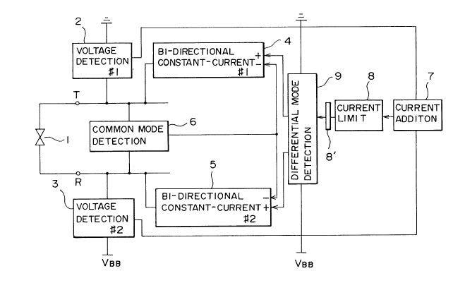
Referring to FIG.2, a feed current is supplied
to the telephone set 1 via the 2-wire telecommunication
line formed of the TIP line and the RING line in the
same manner as that in a case shown in FIG.1. A first
2077 522
1 voltage detection circuit 2 detects a voltage VTG across
the TIP line and the ground line and outputs a first
detecting current corresponding to the detected
voltage. A second voltage detection circuit 3 detects a
voltage VRB across the RING line and the power line
(VBB) of the power supply for this battery feed circuit
and outputs a second detecting current corresponding to
the detected voltage. The TIP line is connected with an
output of a first bi-directional constant-current
circuit 4. The RING line is connected with an output of
a second bi-directional constant-current circuit 5. A
common mode signal detection circuit 6 is coupled to the
TIP line and the RING line and detects common mode
signals on the TIP line and the RING line. An output of
the common mode signal detection circuit 6 is supplied
to common input terminals (-) of both the bi-directional
constant-current circuits 4 and 5. The first detecting
current output from the first voltage detection circuit
2 and the second detecting current output from the
second voltage detection circuit 3 are supplied to a
current addition circuit 7. The current addition
circuit 7 superposes the first and second voltage
detecting currents. An output current of the current
addition circuit 7 is supplied to a differential voltage
output circuit 9 via a current limit circuit 8 for
limiting the current to a value less than a
predetermined value and a low pass filter 8' for
removing an AC component from the current. The
differential voltage output circuit 9 is connected to
the ground line and the power line (VBB) and outputs a
pair of first and second differential voltages. The
first differential voltage is greater than VBB/2 and the
second differential voltage is less than VBB/2.
Absolute differences between the first differential
voltage and VBB/2, and between the second differential
voltage and VBB/2 are equal to each other and depend on
the output current of the current addition circuit 7.
207752~
1 The first and second differential voltages from the
differential voltage output circuit 9 are respectively
supplied to terminals (+) of the first and second
bi-directional constant-current circuits 4 and 5.
In the above battery feed circuit, the
voltages between the TIP line and the ground line and
between the RING line and the power line (VBB) are
detected by the first and the second voltage detection
circuits 2 and 3. Then the feed current to be supplied
to the telephone set 1 is controlled based on currents
depending on the above voltages detected by the first
and second voltage detection circuits 2 and 3. In this
case, the battery feed circuit has a resistance
characteristic. In an equivalent circuit of the battery
feed circuit regarding either the TIP line or the RING
line, shown in FIG.3, when a voltage VA is supplied to a
line, the voltage detection circuit VD detects the
voltage VA on the line and outputs a detecting current
ia having a value of one K-th (l/K) of a value of the
detected voltage. A constant-current source I outputs a
current IA having a value N times the value of the
detecting current ia. The detecting current ia and the
current IA output from the constant-current source I are
respectively denoted by the following formulas.5
ia = VA/K
IA = ia x N = (VA/K) x N
Here, Ra (=VA/IA) is an equivalent resistance and30 denoted by the following formula.
Ra = VA/IA = VA/[(VA/K) x N]
= K/N
That is, the equivalent resistance Ra is equal to a
constant value K/N. Thus, the battery feed circuit has
a constant resistance characteristic.
-- 10
207752~
1 When the feed current supplied to the
telephone increases, the current limit circuit 8 limits
the feed current to a value less than a predetermined
value. As the bi-directional constant-current circuits
4 and 5 are constant-current sources, the battery feed
circuit operates at a high output impedance with respect
to differential mode signals on the TIP line and the
RING line. The common mode signal detection circuit 6
detects a voltage at a node between the TIP line and the
RING line and the detected voltage is fed back to the
common terminals (-) of both the bi-directional
constant-current circuits 4 and 5, so that the output
currents of the bi-directional constant-current circuits
4 and 5 are controlled so as to be in proportion to the
magnitude of the common mode signal. As a result, the
battery feed circuit operates at a low impedance with
respect to common mode signals on the TIP line and RING
line.
A description will now be given, with
reference to FIGS.4, 5A, 5B and 6, of a first embodiment
of the present invention.
Referring to FIG.4, which shows a circuit
structure of a battery feed circuit according to the
first embodiment of the present invention, the battery
feed circuit comprises the first and second detection
circuits 2 and 3, the first and second bi-directional
constant-current circuits 4 and 5, the common signal
detection circuit 6, the current addition circuit 7, the
current limit circuit 8, the low pass filter 8' and the
differential voltage output circuit 9, in the same
manner as that shown in FIG. 2.
Each of the first and second bi-directional
constant-current circuits 4 and 5 is formed of a
transconductance amplifier. The transconductance
amplifier outputs a current in proportion to an input
voltage regardless of an electric potential on a line
(the TIP line or the RING line) connected therewith.
ll ~ ~
20 7752~
1 Thus, an output impedance of the transconductance
amplifier is very high. The common mode signal
detection circuit 6 has a pair of resistors Rc
respectively connected to the TIP line and the RING line
and a resistor Rd connected between VBB/2 and a node
between the resistors Rc. Due to the pair of resistors
Rc and the resistor Rd, the common mode signal detection
circuit 6 detects a voltage at the node between the
resistors Rc. The voltage detected at the node between
the resistors Rc corresponds to a common mode signal.
The common mode signal detection circuit 6 outputs a
voltage depending on the detected voltage. The output
voltage of the common mode signal detection circuit 6 is
supplied to the negative input terminals of both the
bi-directional constant-current circuits 4 and 5. Thus,
a common mode impedance in each of the TIP line and the
RING line is small. The common mode impedance depends
on a ratio of the resistors Rc to Rd and a voltage to
current conversion ratio of the transconductance
amplifier. The common mode impedance is approximately
equal, for example, to 50 ohms. The common mode
impedance can be freely changed by variation of values
of the resistors Rc, Rd and transconductances of the
bi-directional constant-current circuits.
The first voltage detection circuit 2
comprises a mirror circuit M1 and a resistor Rb. The
resistor Rb is connected to the TIP line and an input
terminal of the mirror circuit M1. In general, a mirror
circuit is constructed of transistors and resistors as
shown in FIG.5A and indicated by a symbol shown in
FIG.5B. The mirror circuit outputs a current, from an
output terminal, equal to an input current supplied to
an input terminal. A current depending on the voltage
VTG across the TIP line and the ground line is supplied
via the resistor Rb to the input terminal of the mirror
circuit M1 of the first voltage detection circuit 2.
The mirror circuit M1 outputs a current equal to the
- 12 -
2077522
1 input current, so that the first voltage detection
circuit 2 outputs the current approximately in
proportion to the voltage VTG. The second voltage
detection circuit 3 comprises a mirror circuit M2 and a
resistor Rb connected to the RING line and an input
terminal of the mirror circuit M2. The second voltage
detection circuit 3 outputs a current approximately in
proportion to the voltage VRB across the RING line and
the power line (VBB), in the same manner as the first
voltage detection circuit 2. The output currents of the
first and second voltage detection circuits 4 and 5 are
supplied to the current addition circuit 7.
The current addition circuit 7 has a mirror
circuit M3. The current output from the first voltage
detection circuit 2 is supplied to an input terminal of
the mirror circuit M3 and the current output from the
second voltage detection circuit 3 is supplied to an
output terminal of the mirror circuit M3, so that the
currents output from the first and second voltage
detection circuits 4 and 5 are superposed on each other
at the output terminal of the mirror circuit M3.
The current from the output terminal of the
mirror circuit M3 of the current additional circuit 7 is
supplied to the current limit circuit 8. The current
circuit 8 comprises transistors Q1 and Q2, a resistor Rt
and a reference voltage supply VL. Base-emitter
voltages VBE of both the transistors Q1 and Q2 are
approximately equal to each other. A collector of the
transistor Q1 is connected to the ground line and the
reference voltage supply Vl is provided between a
collector and a base of the transistor Q1. A base of
the transistor Q2 is connected to the ground line, and
an emitter of the transistor Q2 is connected via the
resistor Rt to an emitter of the transistor Q1. An
output current of the current limit circuit 8 is
supplied from a collector of the transistor Q2 to the
low pass filter 8'.
- 13 -
2 0 7 7 ~ 2 2
1 In the current limit circuit 8, when a voltage
drop VRt caused by the input current passing through the
resistor Rt is less than the reference voltage VL, the
transistor is in an off-state and all the input current
passes through the transistor Q2. That is, the input
current is supplied, as it is, to the low pass filter
8'. On the other hand, when the voltage drop VRt
exceeds the reference voltage VL, only an amount of
current corresponding to the reference voltage VL
supplied via the transistor Q2 to the low pass filter 8'
and an amount of current corresponding to a difference
between the voltage drop VRt and the reference voltage
VL passes through the transistor Q1. That is, the
current limit circuit 8 limits the current to be
supplied to the low pass filter to a value equal to or
less than a value corresponding to the reference voltage
VL.
The low pass filter 8' is constituted of a
mirror circuit M4 having transistors Q3 and Q4,
resistors and a capacitor C1. The current supplied from
the current limit circuit 8 is inverted by the
transistors Q3 and Q4 and an AC component in the current
is removed by the capacitor C1 therefrom. Thus, only a
DC component of the current is output from the
transistor Q4. The current output from the transistor
Q4 of the low pass filter 8' is supplied to the
differential voltage detection circuit 9.
The differential voltage detection circuit 9
comprises mirror circuits M5 and M6, first and second
resistors Re and buffer amplifiers 20 and 21. The
current supplied from the current addition circuit 7 via
the current limit circuit 8 and the low pass filter 8'
to the differential voltage output circuit 9 is input to
an input terminal of the mirror circuit M5. The mirror
circuit M5 has first and second output terminals. An
output current from the first output terminal of the
mirror circuit M5 is supplied to an input terminal of
2077522
1 the mirror circuit M6. An output current from an output
terminal of the mirror circuit M6 is supplied to the
first resistor Re connected to VBB/2. An output current
from the second terminal of the mirror circuit M5 is
supplied to the second resistor Re connected to VBB/2.
A voltage generated at the first resistor Re is supplied
to the first bi-directional constant-current circuit 4
via the buffer amplifier 20. A voltage generated at the
second resistor Re is supplied to the second
bi-directional constant-current circuit 5 via the buffer
amplifier 21. Magnitudes of the voltages generated at
the first and second resistors Re are equal to each
other, and polarities of these voltages are opposite to
each other. Each of the voltages generated at the first
and second resistors Re is in proportion to a voltage
(VTG + VBR).
The first and second bi-directional
constant-current circuits 4 and 5 supply the feed
current to the telephone set 1 in accordance with a
characteristic shown in FIG.6. In FIG.6, a
horizontal-axis corresponds to a line resistance and a
longitudinal-axis corresponds to a feed current supplied
to the telephone set 1. A curve fl indicates the
resistance characteristic, and a curve f2 indicates the
current limit characteristics. According to the current
limit characteristic indicated by the curve f2, the feed
current to be supplied to the telephone set 1 is limited
to a limit current of 50mA. This limit current depends
on the resistor Rt and the reference voltage VL in the
current limit circuit 8.
According to the first embodiment, the feed
current is controlled based on the voltages VTG and VRG
respectively between the TIP line and ground line and
between the RING line and the power line (VBB) without
the differential voltage across the TIP line and the
RING line. Thus, if the power voltage VBB on the power
line decreases, the feed current to be supplied to the
- 15 -
2077522
1 telephone set 1 decreases. As a result, the voltages
VTG and VRB are vary almost not at all, and the dynamic
range on the TIP line and the RING line does not
decrease.
A description will now be given of the
principle of a second embodiment of the present
invention with reference to FIG.7. In FIG.7, those
parts which are the same as those shown in FIG.2 are
given the same reference numbers.
Referring to FIG.7, a battery feed circuit
according to the second embodiment has the first and
second voltage detection circuits 2 and 3, the first and
second bi-directional constant current circuits 4 and 5,
the common mode signal detection circuit 6, the current
addition circuit 7, the current limit circuit 8, the low
pass filter 8' and the differential voltage output
circuit 9, in the same manner as that of the first
embodiment shown in FIG.2. The battery feed circuit of
the second embodiment further comprises a 1/N circuit 10
provided between the current addition circuit 7 and the
current limit circuit 8 and a bias circuit 11 provided
between the TIP line and the RING line. The 1/N circuit
10 divides the current output from the current addition
circuit 7 by N. That is, the 1/N circuit 10 outputs a
current one N-th of the current output from the current
addition circuit 7. The bias circuit 11 applies a bias
voltage across the TIP line and the RING line in a state
where the telephone set 1 is in an on-hook condition.
Due to the bias voltage, an idling current passes
through the TIP line and RING line.
In the second embodiment, the battery feed
circuit operates in accordance with the same
characteristics as in the above first embodiment, in the
normal state. Further, according to the battery feed
circuit of the second embodiment, the telephone set 1
can carry out an on-hook transmission operation. The
on-hook transmission operation is defined as an
2077522
1 operation in which signals equivalent to voice signals
are transmitted from the subscriber circuit to remote
subscriber stations with the telephone set 1 in the
on-hook state. That is, when the telephone set 1 is in
the on-hook state, the TIP line and the RING line are
biased by the bias circuit 11. Due to the biasing of
the TIP line and the RING line, the on-hook transmission
operation can be carried out. The output current from
the current addition circuit 7 is divided by N by the
1/N circuit 10, so that the equivalent resistance of
this battery feed circuit increases N times. Thus, even
if the idling current supplied from the bias circuit 11
to the TIP line and the RING line is small, the
necessary bias voltage can be applied across the TIP
line and the RING line.
A description will now be given, with
reference to FIGS.8, 9A, 9B, 10 and 11, of the second
embodiment of the present invention.
FIG.8 shows a circuit structure of a battery
feed circuit according to the second embodiment of the
present invention. In FIG.8 those parts which are the
same as those shown in FIG.4 are given the same
reference numbers.
Referring to FIG.8, the battery feed circuit
comprises the first and second voltage detection
circuits 2 and 3, the first and second bi-directional
constant-current circuit 4 and 5, the common mode signal
detection circuit 6, the current addition circuit 7, the
current limit circuit 8, the low pass filter 8' and the
differential mode signal detection circuit 9. The ltN
circuit 10 is provided between the current addition
circuit 7 and the current limit circuit 8, so that the
current output from the current addition circuit 7 is
divided by N and a current one N-th of the current
output from the current addition circuit 7 is supplied
to the current limit circuit 8. The bias circuit 11 is
connected to the TIP line and the RING line so that an
20 7 75 22
1 idling current is supplied from the bias circuit 11 to
the TIP line and the RING line when the telephone set 1
is in the on-hook state.
In the on-hook transmission operation, an
equivalent circuit of the battery sheet circuit is shown
in FIG.9A. In FIG.9A, feed current resistances are
indicated by RA and RB. As no current passes through
the TIP line and the RING line in the on-hook state,
voltages are not generated at the feed current resistors
RA and RB. The feed current resistors RA and RB are
generally formed of electronic circuits, a predetermined
bias voltage being required to transmit signals from the
feed current resistors RA and RB, it is thus necessary
to supply a predetermined current (an idling current) to
the TIP line and the RING line. In FIG.sA, an inductive
coupling of an AC power supply with respect to the
2-wire telecommunication line (the TIP line and the RING
line) is shown. As shown in FIG.9A, supplying an
induced voltage to the line in the common mode is
referred to as an AC induction. Under a standard such
as LSSGR, an amount of current cased by the AC induction
is 12 mA (a peak value) in each of the TIP and RING
lines. Thus, in a case where a battery feed circuit
equivalently indicated by the current feed resistors RA
and RB can make pass a current in one direction, an
idling current greater than 12 mA (e.g. 15 mA) has to be
supplied to the TIP line and RING line.
In the second embodiment of the present
invention, as the battery feed circuit comprises the
bi-directional constant-current circuits 4 and 5, the
idling current can decrease so long as the bias voltage
is maintained at a predetermined value. That is, as
shown in FIG.9B, even if the idling current decreases
one ~'-th (e.g. l/5), the necessary bias voltage can be
obtained by increasing the feed current resistances RA
and RB N times (e.g. 5 times). In this case, the common
impedance is set at a value (e.g. 50 ohms) less than a
2077522
- 18 -
1 value (e.g. 200 ohms) of the DC impedance, and the bias
voltage is ensured for a voltage drop caused by the AC
induced current of 12 mA and signals in the on-hook
transmission operation.
A control of the feed current resistance will
be described below with reference to FIG.10.
Referring to FIG.10, the battery feed circuit
includes the first and second bi-directional
constant-current circuits 4 and 5. The common mode
signal detection circuit 6 detects a common mode
impedance at a node between resistors R respectively
connected to the TIP line and the RING line. The
detected common mode impedance is fed back to the
bi-directional constant-current circuits 4 and 5.
Further, output currents from the voltage detection
circuits 2 and 3 are added to each other, the l/N
circuit 10 divides the result obtained by addition of
the currents by N and outputs a 1/N current. Then, the
l/N current output from the 1/N circuit 10 is fed back
to the bi-directional constant-current circuits 4 and 5.
In a normal state, N is set to 1 (N = 1) in
the l/N circuit lO and the feed current resistance is
approximately 200 ohms. In the on-hook transmission
operation, N is set to 5 (N = 5) in the l/N circuit lO
and the feed current resistance is approximately lO00 (=
200 x 5) ohms. Thus, in the on-hook transmission
operation, even if the idling current of 3 mA is
supplied to the TIP line and the RING line, the bias
voltage having a value corresponding to a current of 15
mA is ensured.
The battery feed circuit shown in FIG.8
operates in the same manner as the equivalent circuit
shown in FIG.10. Signals RCV to be transmitted to
remote stations are input to this battery feed circuit
via the differential mode signals detection circuit 9.
In the normal state, the battery feed circuit shown in
FIG.8 supplies the feed current to the telephone set l
207 7 5 22
-- 19
1 in the same manner as that shown in FIG.4.
The 1/N circuit 10 is formed as shown, for
example, in FIG.ll.
Referring to FIG.ll, the l/N circuit 10
comprises a switching part 20 (SW) having transistors Q7
and Q8 and a dividing part 21 (1/N) having transistors
Q5 and Q6 and resistors Rna and Rnb. A control signal
Vin is supplied to the transistor Q7 of the switching
part 20. When a level of the control signal Vin is
greater than a predetermined threshold level Vth (Vin i~
Vth), the transistor Q7 is turned on and the transistor
Q8 is turned off. When the level of the control signal
Vin is less than the threshold level Vth (Vin ~ Vth),
the transistor Q7 is turned off and the transistor Q8 is
turned on. The transistors Q5 and Q6 and the resistors
Rna and Rnb in the dividing part 21 form a mirror
circuit. The resistances Rna and Rnb are set so that
the following equation of proportionality is satisfied.
Rna : Rnb = 1 : N-l
Thus, proportionality of currents respectively passing
through the transistors Q5 and Q6 is equal to N-1 : 1.
When the transistor Q8 in the switching part 20 is
turned on, both the currents in the transistors Q5 and
Q6 are output from the 1/N circuit 10. On the other
hand, when the transistor Q8 is turned off, all the
current in the transistor Q5 is supplied to the
transistor Q7 in the switching part 20 and only the
current in the transistor Q6 is output from the 1/N
circuit 10. Thus, in this case, the l/N current is
output from the l/N circuit 10. That is, in the normal
state, the control signal Vin having the level less than
the threshold level Vth is supplied to the switching
part 20. In the on-hook transmission operation, the
control signal Vin having the level greater than the
threshold level Vth is supplied to the switching part 20.
2077522
- 20 - - __
1 According to the second embodiment, in the
on-hook transmission operation, the 1/N circuit 10
decreases to one N-th the current to be fed back to the
bi-directional constant-current circuits 4 and 5. Thus,
an idling current required for the on-hook transmission
operation can be decreased.
The present invention is not limited to the
aforementioned embodiments, and variations and
modifications may be made without departing from the
scope of the claimed invention.