Note: Descriptions are shown in the official language in which they were submitted.
2077602
A LOW VOLTAGE SWING OUTPUT MOS
CIRCUIT FOR DRIVING AN ECL CIRCUIT
BACKGROUND OF THE INVENTION
This invention relates to electronic circuitry and,
more particularly, to a MOS circuit for driving an ECL
circuit.
Fig. 1 is a block diagram of a portion of a
conventional computing system 10. Computing system 10
comprises a central processing unit (CPU) 14 for processing
instructions and data, a cache memory 18 for storing pages of
data for high speed access by CPU 14, and a floating point
unit (FPU) 22 for performing arithmetic operations on floating
point data from cache memory 18. CPU 14 communicates data to
cache memory 18 over a CPU-cache bus 26 and receives data from
cache memory 18 over a cache-CPU bus 30. FPU 22 also receives
data from cache memory 18 over a cache-FPU bus 34 which is
coupled to cache-CPU bus 30. CPU 14 communicates with FPU 22
over a CPU-FPU bus 38.
Since cache memory 18 is intended to provide high
speed access to data, it should be constructed with circuit
elements which respond quickly to the signals used to access
the data. Emitter coupled logic (ECL) circuits often meet the
performance requirements of such high speed applications, so
they are often used in cache memory designs. Fig. 2 is a
schematic diagram of a conventional ECL gate 42 which may be
used alone or in conjunction with other circuitry to meet the
needs of a particular high speed circuit. ECL gate 42
64157-384
2 2077602
comprises a first bipolar transistor 46 and a second bipolar
transistor 50. Emitters 52, 54 of transistors 46 and 50 are
coupled together and, through a resistor R3, to a ground
potential. A collector 62 of transistor 46 is coupled to a
voltage (and current) source Vcc through a resistor R1.
Similarly, a collector 66 of transistor 50 is coupled to Vcc
through a resistor R2. A base terminal 70 of transistor 50 is
coupled to a reference voltage VREF, and a base terminal 74 of
transistor 46 is coupled to a control input voltage VIN. In a
differential ECL gate receiving a differential input voltage,
the reference voltage VREF is the complement of the input
voltage VIN.
ECL gate 42 is controlled so that current always
flows from Vcc, through transistor 46 or 50, and to ground.
Which transistor 46 or 50 conducts the current depends upon
the magnitude of VIN relative to VREF- If VIN is positive
relative to VREF, then current flows through transistor 46,
and if VREF is positive relative to VIN, then current flows
through transistor 50.
Current flow through either transistor 46 or
transistor 50 causes a voltage drop of approximately 0.6
volts, across resistors R1 or R2, respectively. For example,
when current flows through transistor 46, the voltage at
collector 62 is approximately Vcc ~ 0.6 volts. Consequently,
when VIN equals Vcc ~ 0.6 volts, transistor 46 is on the edge
of saturation. If VIN is greater than Vcc - 0.6 volts, then
- transistor 46 is saturated, the base is
~, ,
~ . ,~
64157-384
2a 2077602
forward biased with respect to the collector, and extra charge
is stored in the base. Unfortunately, when a signal is
supplied to the base terminal of a saturated transistor to
turn the transistor off, the extra charge in the base must be
dissipated before the transistor can turn off, and the delay
may be unacceptable. Therefore, the driving circuit should
prevent saturation by keeping VIN from going more positive
than Vcc ~ 0.6 volts. In a typical ECL circuit, Vcc equals 0
volts and ground equals -5 volts. Thus, VIN should not be
greater (more positive) than -.6 volts.
In the computing circuit shown in Fig. 1, CPU 14 may
be constructed with metal oxide semiconductor (MOS) circuit
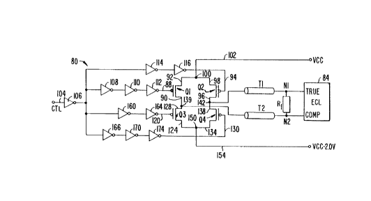
elements. Fig. 3 is a schematic diagram of a MOS circuit 80,
not necessarily in the prior art, for driving one or more ECL
gates 42 shown generally as an ECL circuit 84. ECL circuit 84
may be a part of cache memory 18. MOS driver 80 includes PMOS
- 64157-384
~77602
transistors Q1, Q2, Q3, and Q4. Transistor Q1 has a gate
terminal 88, a current flowing terminal 90, and a current
flowing terminal 92. Similarly, transistor Q2 includes a gate
terminal 94, a current flowing terminal 96, and a current
flowing terminal 98. The current flowing terminal 92 of
transistor Q1 is coupled to the current flowing terminal 98 of
transistor Q2 at a first voltage node 100. First voltage node
100 is coupled to a voltage (and current) source Vcc through a
line 102. Gate terminal 88 of transistor Q1 is coupled for
receiving control signals applied to a line 104 through
inverters 106, 108, 110, and 112. Gate terminal 94 of
transistor Q2 receives the control signals applied to line 104
through inverters 106, 114 and 116. The signal applied to gate
terminal 88 is thus an inverted copy of the signal applied to
gate terminal 94.
Transistor Q3 has a gate terminal 120, a current
flowing terminal 124, and a current flowing terminal 128.
Similarly, transistor Q4 has a gate terminal 130, a current
flowing terminal 134, and a current flowing terminal 138.
Current flowing terminal 128 of transistor Q3 is coupled to
current flowing terminal 90 of transistor Q1 at a node 139.
Similarly, current flowing terminal 138 of transistor Q4 is
coupled to current flowing terminal 96 of transistor Q2 at a
node 142. Current flowing terminals 124 and 134 are coupled
together at a second voltage node 150 which, in turn, is
coupled to a voltage Vcc ~ 2.0 volts through a line 154. Gate
terminal 120 of transistor Q3 receives the control signals
applied to line 104 through inverters 106, 160, and 164. Gate
terminal 130 of transistor Q4 receives the control signals
applied to line 104 through inverters 106, 166, 170, and 174.
A transmission line T1 is coupled to node 142 and to
the true input terminal of differential ECL circuit 84, whereas
a second transmission line T2 is coupled to node 139 and to the
complement input terminal of differential ECL circuit 84. The
signals at nodes N1 and N2 may be used as the true and
complement VIN signals for ECL gates 42 in ECL circuit 84. A
terminating resistor RT is coupled between transmission line T1
20~7~0~
and transmission line T2 for preventing reflections along
transmission line T1 or transmission line T2. If the
transmission lines have an impedance of 50 ohms, the correct
value for RT to prevent reflections is 100 ohms, and this value
will be assumed hereafter. Separate terminating resistors (of
50 ohms, not shown) for each transmission line are sometimes
used for this purpose as well.
In operation, either transistors Q1 and Q4 or
transistors Q2 and Q3 are conducting at any given time. When
transistors Q1 and Q4 are conducting, current flows along line
102, through transistor Q1, through transmission line T2,
through termination resistor RT, through transmission line T1,
through transistor Q4, and through line 154. When transistors
Q2 and Q3 are conducting, then current flows through line 102,
through transistor Q2, through transmission line Tl, through
termination resistor RT' through transmission line T2, through
transistor Q3, and through line 154. In any event, current
always flows through line 102, through node 100, to node 150,
and through line 154, and complementary output signals appear
at nodes 139 and 142.
Fig. 4 is a schematic diagram showing a resistor
circuit 180 that is the equivalent of circuit 80 shown in Fig.
3. A resistor RQl2 represents the resistance through either
transistor Q1 or transistor Q2, depending on which transistor
is conducting at the time. Similarly, a resistor RQ34
represents the resistance through either transistor Q3 or
transistor Q4, again depending upon which transistor is
conducting. Given a voltage of Vcc at the upper portion of the
circuit and a voltage of Vcc ~ 2 volts at the lower portion of
the circuit, then the voltage drop across the series of
resistances is equal to -2 volts. To limit the voltage at node
Nl to -.6 volts (to avoid saturating the ECL transistors as
discussed above), and assuming RQ12 equals RQ34 equals R, then
the required resistance of transistors Q1-Q4 may be determined
by solving the equation R/(2R + 100) X (-2) volts = -.6 volts.
That is, the resistance R of each transistor Q1-Q4 should be 75
ohms or greater.
2077602
It is common for the resistance of transistors to
vary by up to a factor of 4, depending on operating voltage,
temperature, process variations during manufacturing, etc.
Thus, a transistor having a minimum resistance of 75 ohms, to
satisfy the maximum 0.6 volt requirement, may have a maximum
resistance of 300 ohms. Such a resistance still satisfies the
-0.6 volt limitation at node Nl, but then the total voltage
swing across resistor RT is only approximately 0.28 volts,
which provides a very weak differential signal across nodes Nl
and N2. A desirable voltage swing is approximately 0.6 volts
or more. If the transistors are designed to provide a 0.6
volt swing when the transistors are weak (high resistance),
then, when the transistors are strong (low resistance), the
voltage at node Nl would rise above the -0.6 volt maximum,
thus saturating the ECL transistors.
SUMMARY OF THE INVENTION
The present invention is directed to a MOS driver
for an ECL circuit which avoids saturating the driven ECL
circuit elements while maintaining a strong differential
output signal for both weak or strong MOS transistors. In one
embodiment of the present invention, first, second, third and
fourth MOS transistors each have a gate terminal, a first
current flowing terminal, and a second current flowing
terminal. The first current flowing terminal of the first MOS
transistor is coupled to the first current flowing terminal of
the second MOS transistor at a first voltage node; the first
current flowing terminal of the third MOS transistor is
64157-384
5a 2077602
coupled to the second current flowing terminal of the first
MOS transistor at a first output node; the first current
flowing terminal of the fourth MOS transistor is coupled to
the second current flowing terminal of the second MOS
transistor at a second output node; and the second current
flowing terminal of the fourth MOS transistor is coupled to
the second current flowing terminal of the third MOS
transistor at a second voltage node. A transistor control
unit is coupled to the gate terminals of the first, second,
third and fourth MOS transistors for biasing the
64157-384
6a 2077602
transistor and the second transistor so that complementary
signals are provided at the first output node and the second
output node; a resistance coupled in series with the first
current flowing terminal of the first transistor and the first
current flowing terminal of the second transistor; and wherein
the resistance is connected so that current flows through the
resistance whenever current flows through either the first
current flowing terminal of the first transistor or through
the first current flowing terminal of the second transistor.
According to another broad aspect of the invention
there is provided a circuit for driving an ECL circuit
comprising: a first transistor having a control terminal, a
first current flowing terminal and a second current flowing
terminal; a second transistor having a control terminal, a
first current flowing terminal and a second current flowing
terminal; wherein the first current flowing terminal of the
first transistor is coupled to the first current flowing
terminal of the second transistor at a first voltage node; a
third transistor having a control terminal, a first current
flowing terminal and a second current flowing terminal;
wherein the first current flowing terminal of the third
transistor is coupled to the second current flowing terminal
of the first transistor at a first output node; a fourth
transistor having a control terminal, a first current flowing
terminal and a second current flowing terminal; wherein the
second current flowing terminal of the fourth transistor is
64157-384
6b 2077602
coupled to the second current flowing terminal of the third
transistor at a second voltage node; wherein the first current
flowing terminal of the fourth transistor is coupled to the
second current flowing terminal of the second transistor at a
second output node; a resistance coupled between the first
voltage node and a current source; and transistor control
means, coupled to the control terminal of the first
transistor, to the control terminal of the second transistor,
to the control terminal of the third transistor and to the
control terminal of the fourth transistor for biasing the
first transistor, the second transistor, the third transistor
and the fourth transistor for alternately flowing current
through the first transistor and the fourth transistor or
through the second transistor and the third transistor.
According to another broad aspect of the invention
there-is provided an MOS circuit for driving an ECL circuit
comprising: a first MOS transistor having a gate terminal, a
first current flowing terminal, and a second current flowing
terminal; a second MOS transistor having a gate terminal, a
first current flowing terminal, and a second current flowing
terminal; wherein the first current flowing terminal of the
first MOS transistor is coupled to the first current flowing
terminal of the second MOS transistor at a first voltage node;
a third MOS transistor having a gate terminal, a first current
flowing terminal, and a second current flowing terminal;
wherein the first current flowing terminal of the third MOS
64157-384
6c 2077602
transistor is coupled to the second current flowing terminal
of the first MOS transistor at a first output node; a fourth
~ MOS transistor having a gate terminal, a first current flowing
terminal, and a second current flowing terminal; wherein the
first current flowing terminal of the fourth MOS transistor is
coupled to the second current flowing terminal of the second
MOS transistor at a second output node; wherein the second
current
~..
64157-384
J 2077602
6~ 64157-384
flowing terminal of the fourth MOS transistor is coupled to the
second current flowing terminal of the third MOS transistor at a
second voltage node; a first resistance coupled between the first
voltage node and a current source; transistor control means,
coupled to the gate terminal of the first MOS transistor, to the
gate terminal of the second MOS transistor, to the gate terminal
of the third MOS transistor, and to the gate terminal of the
fourth MOS transistor, for biasing the first MOS transistor, the
second MOS transistor, the third MOS transistor, and the fourth
MOS transistor for alternately flowing current through the first
MOS transistor and the fourth MOS transistor or through the second
MOS transistor and the third MOS transistor.
BRIEF DESCRIPTION OF THE DRAWINGS
Figure 1 is a block diagram of a conventional computing
system;
Figure 2 is a schematic diagram of a typical ECL gate
circult;
Figure 3 is a schematic diagram of a MOS circuit for
driving an ECL circuit;
Figure 4 is a schematic diagram of an equivalent
resistance circuit corresponding to the circuit shown in Figure 3;
Figure 5 is a schematic diagram of a particular
embodiment of a MOS circuit according to the present invention for
driving an ECL circuit; and
Figure 6 is a schematic diagram of an equivalent
resistance circuit corresponding to the circuit shown in Figure 5.
~077~2
DESCRIPTION OF THE PREFERRED EMBODIMENT
Fig. 5 is a schematic diagram of a particular
embodiment of a MOS driver 200 according to the present
invention for driving ECL circuit 84. The components which are
the same as circuit 80 of Fig. 3 are numbered the same. In
this embodiment, a source resistance Rs is disposed between
voltage (current) source Vcc and node 100 so that current flows
through source resistance Rs whenever current flows through
transistors Q1 or Q2.
Fig. 6 is a schematic diagram of an equivalent
resistance circuit corresponding to the circuit shown in
Fig. 5. The elements which are the same as those shown in Fig.
4 are labeled the same. As shown, source resistance Rs (e.g, a
resistor) is connected in series with resistances RQ12, RT, and
RQ34. Assuming a source resistance (Rs) value of 50 ohms, and
a termination resistance RT value of 100 ohms, then the
resistance of transistors Q1-Q4 may be 0 ohms and the voltage
at node Nl still meets the upper voltage limit of -0.6 volts to
avoid saturating the ECL transistors. Thus, transistors having
any resistance value may be used without exceeding the upper
voltage limit (assuming RQl2 is about equal to RQ34).
Now assume transistors having an expected resistance
value of 25 ohms each are used for transistors Q1-04. If so,
then the voltage at node 100 is approximately -.5 volts, the
voltage at node N1 is approximately -.75 volts, and the voltage
at node N2 is approximately -1.75 volts. The voltage at node
N1 is not more positive than the -0.6 volt maximum, and the
total voltage swing across resistor RT (and nodes Nl and N2) is
approximately 1 volt.
Assuming a worst case resistance variation by a
factor of 4 for all transistors, then the maximum resistance of
transistors Q1-Q4 is approximately 100 ohms. In that case, the
voltage at node 100 is approximately -.29 volts, the voltage at
node N1 is approximately -.86 volts, and the voltage at node N2
is approximately -1.43, volts. The upper voltage limit of
-0.6 volts at node N1 is maintained, and the total voltage
swing across resistor RT is approximately +.57 volts.
2~3776~
In either case, source resistance Rs ensures that
saturation of the driven ECL transistors is avoided while
maintaining a strong differential signal across nodes Nl and
N2.
It should be noted that source resistance RS
functions as a negative feedback element so that if transistors
Ql-Q4 are strong (e.g., a resistance value of approximately 25
ohms), then the supply voltage at node 100 is relatively low
(approximately -.5 volts). However, if transistors Ql-Q4 are
weak (e.g., a resistance value of approximately 100 ohms), then
the supply voltage at node 100 is higher (-.29 volts).
While the above is a complete description of a
preferred embodiment of the present invention, various
modifications may be employed. For example, a plurality of MOS
driver circuits may be coupled in parallel using a single
source resistance Rs. In that case, the source resistance Rs
would be adjusted to meet the requirements of the parallel
circuits. In the case of five driver circuits, the original 50
ohm source resistance would be replaced by a 10 ohm source
resistance. Consequently, the scope of the invention should be
ascertained by the claims.