Note: Descriptions are shown in the official language in which they were submitted.
2077873
~'' ~'il'"'
PATENT APPLICATION
Attorney Docket No. D/91181
RESISTIVE INTERMEDIATE TRANSFER MEMBER
The present invention relates generally to a system for transfer
of charged toner particles in an electrostatographic printing apparatus, and
more particularly concerns an apparatus for enabling an intermediate
transfer member having a laterally conductive resistive backing substrate.
Generally, the process of electrostatographic copying is executed
by exposing a light image of an original document onto a substantially
uniformly charged photoreceptive member. Exposing the charged
photoreceptive member to a light image discharges a photoconductive
surface thereon in areas corresponding to non-image areas in the original
document while maintaining the charge in image areas, thereby creating
an electrostatic latent image of the original document on the
photoreceptive member. Charged developing material is subsequently
deposited onto the photoreceptive member such that the developing
material is attracted to the charged image areas on the photoconductive
surface thereof to develop the electrostatic latent image into a visible
image. The developing material is then transferred from the
photoreceptive member, either directly or after an intermediate transfer
step, to a copy sheet or other support substrate, creating an image which
may be permanentiy affixed to the copy sheet to provide a reproduction of
the original document. In a final step, the photoconductive surface of the
photoreceptive member is cleaned to remove any residual developing
material thereon in preparation for successive imaging cycles.
The described electrostatographic copying process is well known
and is commonly used for light lens copying of an original document.
Analogous processes also exist in other electrostatographic printing
applications such as, for example, ionographic printing and reproduction,
where charge is deposited in an image pattern on a charge retentive
surface in response to electronically generated or stored images as
2û77 7 )
described in U.S. Patent Nos. 3,564,556; 4,240,084; and 4,619,515 among
others.
The process of transferring developing material from an image support
surface to a second supporting surface is realized at a transfer station. In a
conventional transfer station, transfer is achieved by applying electrostatic
force fields in a transfer region sufficient to overcome forces which hold the
toner particles to the photoconductive surface on the photoreceptive member.
These electrostatic force fields operate to attract and transfer the toner
o particles over onto the second supporting surface which may be an
intermediate transfer belt or an output copy sheet. An intermediate transfer
belt is desirable for use in tandem color or one pass paper duplex (OPPD)
applications where successive toner powder images are transferred onto a
single copy sheet For example, U.S. Patent No. 3,957,367 issued to Goel
teaches a color electrostatographic printing machine wherein successive
single-color powder images are transferred to an intermediary, in
superimposed registration with one another. The resultant multi-layered
powder image is subsequently transferred to a sheet of support material to
form a color copy of an original document Color and OPPD systems may
2 o also utilize multiple photoconductive drums in lieu of a single
photoconductive drum.
Intermediate transfer elements employed in imaging systems of the
type in which a developed image is first transferred from the imaging
member to an intermediate member and then transferred from the
2 5 intermediate to an outer copy substrate should exhibit efficient transfer
characteristics both for transfer of the developer material from the imaging
member to the intermediate as well as for transfer of the developer material
from the intermediate to the output copy subskate. Efficient transfer occurs
when most or all of the developer material comprising the developed image
3 o is transferred and little residual developer remains on the surface from which
the image was transferred. Highly efficient transfer is particularly important
when the imaging process entails the creation of full color images by
sequentially generating and developing successive images
- 2 -
2077873
~,_
in each primary color and superimposing the ~eveloped primary color
images onto each other during transfer to the substrate. In particular,
undesirable shifting and variation in final colors produced can occur when
the primary color images are not efficiently transferred to the substrate.
Transfer of toner images between support surfaces in
electrostatographic applications is often accomplished via electrostatic
induction using a corotron or other corona generating device. In corona
induced transfer systems, the second supporting surface, an intermediate
support member or a copy sheet is placed in direct contact with the toner
image while the image is supported on the image bearing surface (typically
a photoconductive surface). Transfer is induced by spraying the back of the
second supporting surface with a corona discharge having a charge polarity
opposite that of the toner particles, thereby inducing electrostatic transfer
of the toner particles to the second supporting surface. An exemplary
corotron ion emission transfer system is disclosed in U.S. Patent No.
2,807,233. Alternatively, transfer can be induced by applying a potential
difference between the substrate of a biased member contacting the
second supporting member and the substrate of the image bearing surface
originally supporting the toner image layer.
The critical aspect of the transfer process focuses on applying
and maintaining high intensity electrostatic fields in the transfer region in
order to overcome the adhesive forces acting on the toner particles.
Careful control of these electrostatic fields is required to induce the physicaldetachment and transfer-over of the charged particulate toner materials
from one surface to a second supporting surface without scattering or
smearing of the developer material. This difficult requirement can be met
by carefully tailoring the electrostatic fields across the transfer region so
that the fields are high enough to effect efficient toner transfer while
being low enough so as not to cause arcing, excessive corona generation, or
excessive toner transfer in the regions prior to intimate contact of the
second supporting surface and the toner image. Imprecise and inadvertent
manipulation of these electrostatic fields can create copy or print defects by
2077873
,_
inhibiting toner transfer or by inducing uncontrolled toner transfer,
causing scattering or smearing of the toner particles.
The specific problems associated with successful image transfer
are well known. Variations in conditions, such as second supporting surface
resistivity, contaminants, and changes in the toner charge or in the
adhesive properties of the toner materials, can all effect necessary transfer
parameters. Further, material resistivity and toner properties can change
greatly with humidity and other ambient environmental parameters. In the
pre-transfer or so called pre-nip region, immediately in advance of contact
between the second supporting surface and the developed image,
excessively high transfer fields can result in premature transfer across an air
gap, leading to decreased resolution or blurred images. High transfer fields
in the pre-nip air gap can also cause ionization which may lead to strobing
or other image defects, loss of transfer efficiency, and a lower latitude of
system operating parameters. Conversely, in the post-transfer or so called
post-nip region, at the photoconductor/second supporting surface
separation area, insufficient transfer fields can cause image dropout and
may generate hollow characters. Also, improper ionization in the post-nip
region may cause image stability defects or can create copy sheet detacking
problems. Inducement of variations in desirable field strength across the
transfer region must be balanced against the basic premise that the
transfer fields should be as large as possible in the region directly adjacent
to the transfer nip where the second supporting surface contacts the
developed image so that high transfer efficiency and stable transfer can be
achieved.
In intermediate transfer systems, conductive backed belts are
typically desired because such conductive materials allow for simple
generation of transfer fields via applied biases (e.g., BTR systems). The use
of conductive materials is also desirable to maintain charge uniformity
patterns. Finally, highly conductive materials, such as steel, nickel, etc.,
typically used for intermediate transfer applications tend to be very sturdy,
non-stretch materials. This characteristic is desirable and important for
- 2077873
maintaining proper registration in single-pass intermediate ~elt
configurations.
A typical problern encountered with the use if highly conductive
backed materials in intermediate transfer belt systems arises from the fact
that the highly conductive backing is an equipotential. Thus, a bias applied
to a conductive backed belt in the transfer nip will generate undesirable
transfer fields away from the nip, and particularly in the pre-transfer region
where pre-nip breakdown and air gap transfer can cause toner splatter and
other image quality defects. Although electrostatic fields typically drop
substantially in the pre-nip transfer zone relative to the transfer nip,
seemingly minimal pre-nip fields can cause significant transfer problems.
Further, nominal pre-nip fields under normal conditions can translate to
poor system robustness relative to environmental or parameter changes
such as high humidity, toner adhesive, pile height, etc.
Various approaches and solutions to the problems inherent to
the transfer process and specifically related to systems including an
intermediate transfer member have been proposed. The following
disclosures may be relevant to various aspects of the present invention:
US-A-4,292,386
Patentee: Takano
Issued: September29,1981
US-A-4,494,857
Patentee: Euno et al.
Issued: January22,1985
US-A-4,931,839
Patentee: Tompkinsetal.
Issued: JuneS,1990
US-A-4,994,342
Pat~ntee: Nakayamaetal.
February 19,1991
2077&7~
-
The relevant portions of the foregoing disclosures may be briefly
sl-mmarized as follows:
US-A-4,292,386 discloses a photosensitive drum comprising a hollow
cylinder having a conductive layer formed on the outer periphery of the
hollow cylinder, a low resistance layer formed on the outer periphery of the
conductive layer, and a photosensitive layer formed on the outer peripheral
surface of the low resistance layer.
US-A-4,494,857 discloses an imaging method using a charged
o insulating layer comprising a process which includes a first step for bringing
a pliable contactor having a specific electric resistance into contact with the
insulating layer, and a second step for impressing a voltage on the contactor
in contact with the insulting layer by means of an electrode having another
specific resistance.
US-A-4,931,389 describes a transfer mechanism for a full color, double
transfer electrophotographic print engine. An image receiving web has a
characteristic sheet resistivity which falls within the range of 107 to 1010
ohms/square. A selectively operable system is used to increase dwell time in
the transfer station, yielding the effect of increasing the effective capacitance
2 o of the transfer station. The combination of lower applied voltages and proper
selection of the surface resistivity of the image receiving web provides a
system wherein direct application of the electric field through web contacts
can be used, thus eliminating coronas and the consequent performance
variations.
2 5 US-A-4,994,342 discloses an electrophotographic lithographic printing
plate precursor comprising an undercoating layer and a backing layer, both
having a resistive surface.
In accordance with the present invention, an apparatus for transferring
toner from an image support surface to a substrate is provided, wherein an
3 o intermediate transfer member is positioned to have at least a portion thereof
adjacent the image support surface to define a transfer zone including a pre-
transfer zone, a transfer nip, and a post-transfer zone and means, located
adjacent said pre-transfer zone, are provided for
- 6 -
"_ ' 2Q77~-~3
establishing a first voltage potential on the intermediate transfer member in
the pre-transfer zone while means, located adjacent the transfer zone, are
provided for establishing a second voltage potential on the intermediate
transfer member in the transfer nip. Means, located adjacent the post-transfer
zone may also be provided for establishing a third voltage potential on the
intermediate transfer belt in the post-transfer zone. The intermediate transfer
belt includes a laterally conductive resistive substrate having a sheet
resistivity range between approximately 107 and 1011 ohms/square.
0 In another aspect of the invention, an electrostatographic printing
apparatus is disclosed, comprising a transfer assembly for transferring toner
from an image support surface to a copy substrate wherein the transfer
apparatus includes an intermediate transfer member positioned to have at
least a portion thereof adjacent the image support substrate to define a pre-
transfer zone, a transfer zone, and a post-transfer zone and means, located
adjacent said pre-transfer zone, are provided for establishing a first voltage
potential on the intermediate transfer member in the pre-transfer zone while
means, located adjacent the transfer nip, are provided for establishing a
second voltage potential on the intermediate transfer member in the transfer
2 o nip.
In yet another aspect of the invention, an apparatus for transferring
charged toner particles from an image support surface to a sheet is disclosed,
comprising an intermediate transfer member being adapted to receive toner
particles from the image support surface and to transfer the toner particles
2 5 therefrom to the sheet, wherein the intermediate transfer member includes a
laterally conductive resistive substrate having a resistivity range between
approximately 107 and 1010 ohms/square.
Other aspects of this invention are as follows:
An apparatus for transferring charged toner particles from an image
3 o support surface to substrate comprising:
an intermediate transfer member positioned to have at least a portion
thereof adjacent said image support surface in a transfer zone, defining a
transfer nip, a pre-transfer zone, and a post-transfer zone;
- 7-
--i
.,.
207~7~
_ ,.
means, located adjacent said pre-transfer zone, for applying a first bias
voltage potential to said intermediate transfer member in said pre-transfer
zone so as to minimize transfer fields therein for substantially preventing
transfer of toner particles from the image support surface to said
intermediate transfer member in the pre-transfer zone;
means, located adjacent the transfer nip, for applying a second bias
voltage potential to said intermediate transfer member in said transfer nip so
as to generate high transfer fields therein for attracting toner particles from
o the image support surface to said intermediate transfer member in said
transfer nip;
means, located adjacent said post-transfer zone, for applying a third
bias voltage potential to said intermediate transfer member in said post-
transfer zone so as to optimize transfer fields therein for substantially
minimizing air breakdown in said post-transfer zone;
a constant current source coupled to each of said means for applying a
first voltage potential, said means for applying a second voltage potential and
said means for applying a third voltage potential for providing a constant
current signal thereto; and
2 o at least one conductive element located peripherally adjacent and
downstream of said transfer zone and coupled to said constant current source
for providing a conducffve path from said intermediate transfer belt to said
constant current source so as to electrically isolate said transfer zone on saidintermediate transfer belt.
2 5 An electrostatographic printing apparatus including a transfer
assembly for transferring toner particles from an image support surface to a
substrate, said transfer apparatus comprising:
an intermediate transfer member positioned to have at least a portion
thereof adjacent said image support substrate in a transfer zone, defining a
3 o transfer nip, a pre-transfer zone, and a post-transfer zone;
-7a-
',,, - ~
2077S73
means, located adjacent said pre-transfer zone, for applying a first bias
voltage potential to said intermediate transfer member in said pre-transfer
zone so as to minimize transfer fields therein for substantially preventing
transfer of toner particles from the image support surface to said intermediate
transfer member in the pre-transfer zone;
means, located adjacent the transfer nip, for applying a second bias
voltage potential to said intermediate transfer member in said transfer nip so
as to generate high transfer fields therein for attracting toner particles from
o the image support surface to said intermediate transfer member in said
transfer nip;
means, located adjacent said post-transfer zone, for applying a third
bias voltage potential to said intermediate transfer member in said post-
transfer zone so as to optimize transfer fields therein for substantially
lS minimi7ing air breakdown in said post-transfer zone;
a constant current source coupled to each said means for applying a
first voltage potential, said means for applying a second voltage potential and
said means for applying a third voltage potential for providing a constant
current signal thereto; and
2 o at least one conductive element located peripherally adjacent and
downstream of said transfer zone and coupled to said constant current source
for providing a conductive path from said intermediate transfer belt to said
constant current source so as to electrically isolate said transfer zone on saidintermediate transfer belt.
2 5 These and other aspects of the present invention will become apparent
from the following description in conjunction with the accompanying
drawings, in which:
-7b-
2077873
~.,.,~
FIG. 1 is an enlarged schematic side view of a preferred
embodiment of the transfer assembly of the present invention showing a
pre-transfer biasing device and a transfer nip biasing device;
FIG. 2 is a perspective schematic showing the transfer assembly
of FlG. 1;
FIG. 3 is an enlarged schematic side view showing an alternative
embodiment of the present invention showing a pre-transfer biasing
device, a transfer nip biasing device, and a post-transfer biasing device;
FIG. 4 is a graphic representation showing typical measured
voltage drops along the transfer region as generated by the intermediate
transfer belt system of the present invention; and
FIG. 5 is a schematic elevational view illustrating an exemplary
electrostatographic printing machine incorporating the features of the
present invention.
While the present invention will be described with reference to a
preferred embodiment thereof, it will be understood that the invention is
not to be limited to this preferred embodiment. On the contrary, it is
intended that the present invention cover all alternatives, modifications,
and equivalents as may be included within the spirit and scope of the
invention as defined by the appended claims. Other aspects and features of
the present invention will become apparent as the following detailed
description progresses, with specific reference to the drawings wherein like
reference numerals have been used throughout the drawings to designate
ident-ical elementstherein.
For a general understanding of an exemplary
ele.lr~ tographic printing machine incorporating the features of the
present invention, reference is made to FIG. S which schematically depicts
the various components thereof. It will become apparent from the
following discussion that the transfer assembly of the present invention is
equally well-suited for use in a wide variety of electroreprographic
machines, as well as a variety printing, duplicating and facsimile devices.
Moving initially to a description of FIG. 5, before describing the
specific features of the present invention in detail, the electrophotographic
2077873
,. ...
copying apparatus employs a highly conductive drum 10 having a
photoconductive layer 12 deposited thereon. The photoconductive layer
12 provides an image support surface mounted on the exterior
circumferential surface of drum 10 and entrained thereabout. A series of
processing stations are positioned about drum 10 which is driven in the
direction of arrow 14 at a predetermined speed relative to the other
machine operating mechanisms by a drive motor (not shown), to transport
the photoconductive surface 12 sequentially through each station. Timing
detectors (not shown) sense the rotation of drum 10 and communicate with
machine logic to synchronize the various operations thereof so that the
proper sequence of events is produced at the respective processing stations.
Initially, drum 10 rotates the photoconductive layer 12 through
charging station A. At charging station A, a charging device which may
include a corona generating device, indicated generally by the reference
numeral 16, sprays ions onto photoconductive surface 12 producing a
relatively high substantially uniform charge thereon.
Once charged, drum 10 is rotated to exposure station B where a
light image of an original document is projected onto the charged portion
of the photoconductive surface 12. Exposure station B includes a moving
lens system, generally designated by the reference numeral 18, where an
original document 20 is positioned face down upon a generally planar,
substantially transparent, platen 22 for projection through the lens 18.
Lamps 24 are adapted to move in timed coordination with lens 18 to
incrementally scan successive portions of original document 20. In this
manner, a scanned light image of original document 20 is projected
throu~h lens 18 onto the photoconductive surface of photoconductive
layer 12. This process selectively dissipates the charge on the
photoconductive layer 12 to record an electrostatic latent image
corresponding to the informational areas in original document 20 onto the
photoconductive surface of photoconductive layer 12. While the preceding
description relates to a light lens system, one skilled in the art will
appreciate that other devices, such as a modulated laser beam may be
207787~
employed to selectively discharge the charged portion of the photoconductive
surface to record the electrostatic latent image thereon.
After exposure, drum 10 rotates the electrostatic latent image recorded
on the surface of photoconductive layer 12 to development station C.
Development station C includes a developer unit, generally indicated by the
rererellce numeral 26, comprising a magnetic brush development system for
depositing developing material on the electrostatic latent image. Magnetic
brush development system 26 preferably includes a single developer roller 38
o disposed in a developer housing 40. In the developer housing 40, toner
particles 41 are mixed with carrier beads, generating an electrostatic charge
therebetweeen and causing the toner particles 41 to cling to the carrier beads
to form developing material. Developer roller 38 rotates and attracts the
developing material, forming a magnetic brush having carrier beads and
toner particles magnetically attached thereto. Subsequently, as the magnetic
brush rotates, the developing material is brought into contact with the
photoconductive surface 12, the electrostatic latent image thereon attracts the
charged toner particles 41 of the developing material, and the latent image on
photoconductive surface 12 is developed into a visible image.
2 o At transfer station D, the developed toner image is electrostatically
transferred to an intermediate member or belt indicated generally by the
ref~ellce numeral 28. Belt 28 is entrained about spaced roller 30 and 32,
respectively, being transported thereabout in the direction of arrow 36.
Preferably, belt 28 contacts drum 10 to form a transfer nip where the
2 s developed image on photoconductive surface 12 is transferred on the belt 28.
In the illustrated embodiment, a bias transfer brush 66 and a grounding
brush 68 are provided for tailoring electrostatic fields in the transfer region.The details of the transfer process, and the specific features of the transfer
apparatus of the present invention will be discussed in greater detail with
3 o refel~ellce to FIGS 1-3.
As belt 28 advances in the direction of arrow 36, the toner image
transferred thereto advances to transfer station E where copy sheet 42 is
advanced, in synchronism with the toner image on belt 28, for
3 5 - 10 -
~-3
2077873
transfe~ of the image to output copy sheet. Transfer station E includes a
corona generating device 44 which sprays ions onto the backside of copy
sheet 42 to attract the toner particles from belt 28 to copy sheet 42 in image
configuration. It will be understood that various transfer devices or
systems, including one similar to the transfer system of the present
invention, can be implemented for utilization at transfer station E.
After the toner particles are transferred to copy sheet 42, the
copy sheet advances on conveyor 50 through fusing station G. Fusing
station G includes a radiant heater 52 for radiating sufficient energy onto
the copy sheet to permanently fuse the toner particles thereto in image
configuration. Conveyor belt 50 advances the copy sheet 42, in the
direction of arrow 54, through radiant fuser 52 to catch tray 56 where the
copy sheet 42 may be readily removed by a machine operator.
Invariably, some residual carrier beads and toner particles
remain adhered to photoconductive surface 12 of drum 10 after transfer of
the image to belt 28. These residual particles and carrier beads are
removed from photoconductive surface 12 at cleaning station F. Cleaning
station F includes a flexible, resilient blade 46, having a free end portion
placed in contact with photoconductive layer 12 to remove any material
adhering thereto. Thereafter, lamp 48 is energized to discharge any
residual charge on photoconductive surface 12 in preparation for a
successive imaging cycle.
The foregoing description should be sufficient for the purposes
of the present application for patent to illustrate the general operation of
an electrophotographic copying apparatus incorporating the features of
the present invention. As described, an electrophotographic copying
apparatus may take the form of any of several well known devices or
systems. Variations of specific electrostatographic processing subsystems or
processes may be expected without affecting the operation of the present
invention.
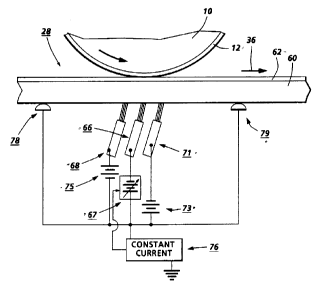
Referring now specifically to FIG. 1, the transfer station of the
present invention and the particular structure thereof will be discussed in
detail. FIG. 1 provides an enlarged detailed view of transfer station D in a
207787~
cross-sectional plane extending along the direction of motion of the
photoconductive drum 10 and perpendicular to the intermediate transfer belt
28. A conventional transfer nip is formed at the point of contact between the
photoconductive imaging surface of the photoconductive layer 12 of
xerographic drum 10 and the intermediate transfer belt 28. The intermediate
transfer belt travels through the nip, moving into and out of engagement with
the imaging surhce of drum 10 wherein the toner powder image thereon is
transferred to the intermediate transfer belt 28. The curvature of the imaging
0 surface of the drum 10 relative to the intermediate transfer belt 28 defines a
transfer zone including a transfer nip as well as a pre-transfer nip air gap anda post-transfer nip air gap located adjacent to the transfer nip along the
upstream and downstream sides thereof, respectively.
The intermediate transfer belt 28 comprises a transferred image
support layer 62 supported on a laterally conductive resistive backing
substrate 60. Transferred image support layer 62 may be comprised of a
photoconductive material or an insulative substrate having a volume
resistivity greater than 5 x 10¹⁰ ohm-cm. Laterally conductive resistive
backing substrate 60 comprises selective materials that permit substantial
2 o charge relaxation during transfer nip dwell time while having sufficient
lateral resistance to allow different potentials to be applied along the length
of the intermediate belt 28. In a preferred embodiment, where typical system
parameters include process speeds of approximately 10 inches/second and
maximum current limitations on the order of 1 mA, a wide sheet resisffvity
range between 107 and 1011 ohms/square and having a volume resistivity less
than approximately 1010 ohm-cm, provides sufficient resistivity. It has been
found that carbon loaded polycarbonate materials can be produced to
provide the desired results for the present invention. However, it will be
understood that various materials and additives can provide suitable
3 o resistivity. For example, tetrahepthlammonium bromide (THAB) ionic
additives have been used successfully as an additive to urethane based
materials in fabricating bias transfer rolls having a specific resistivity. On
going work on materials for use in bias transfer rolls would likely
3s - 12 -
2077873
disclose many alternative materials that would be applicable for use in the
present invention. It is further noted that the intermediate transfer belt 28
of the present invention can be fabricated as a single layer structure so long
as appropriate resistivity is provided.
In a conventional system, electrostatic image transfer from the
xerographic drum 10 to the intermediate transfer belt 28 is typically
accomplished by inducing an electrical transfer field at the transfer nip
located at the point of contact between photoconductive surface 12 and
the intermediate transfer belt 28. The electrical transfer field is typically
generated by a conventional corona generating device or a bias transfer
roll, as is well known in the art, and can be so provided in the present
invention. In the preferred embodiment of the present invention,
electrostatic image transfer to the intermediate transfer belt 28 is
accomplished via a biased blade brush 66 coupled to biasing source 67. The
biased blade brush 66 contacts laterally conductive resistive substrate 60
opposite the transfer nip to provide an applied potential difference
between the intermediate belt 28 and the photoconductor drum 10. The
applied voltage potential of the biased blade 66 in the transfer nip will be
selected to create sufficiently high electrostatic fields of the appropriate
polarity to cause transfer of the toner to the intermediate transfer belt 28.
Typically, fields in the transfer nip that are above 20 volts/micron are
necessary and frequently fields on the order of 40 volts/micron or higher
are required, depending on such factors as toner adhesion, toner charge,
toner mass to be transferred, etc.
It will be noted that a bias potential can be applied to the
conductive substrate of drum 10 to provide a supplemental applied
pote.-l~al difference between the conductive substrate of drum 10 and the
intermediate transfer belt 28 to enhance transfer field generation, as
appropriate. In further discussion herein, the voltages on the conductive
biased blade members acting on the intermediate belt 28 will be assumed
to be referenced to the potential on the conductive substrate of drum 10,
and the reference potential of the conductive substrate of drum 10 will
further be assumed to be zero, strictly for convenience of further
2077873
discussion. It will be appreciated by those of skill in the art that, although
the present discussion refers to a nphotoconductor drum" as the toner
image bearing member, a photoconductor belt might also act as the irnage
bearing mernber in this invention. It will be further appreciated that
various other structures such as sufficiently conductive shim blades, brush
rollers, spongy rollers, etc. can be used as an alternative to the blade
brushes of the preferred embodiment.
Although the applied potential difference between the transfer
nip blade brush 66 and the conductive substrate of drum 10 contribute to
the generation of transfer fields, it will be recognized that any bound
surface charge present on the photoconductor 12 surface and on the
intermediate transfer belt 28 surface will also contribute to the fields
created in and around the transfer zone. The relative contribution of the
applied voltage terms and the surface charge related terms to the transfer
fields can be readily described by the equation:
VE = VB + V2 V3
which refers to an "effective applied potentialn (VE) for the system, as
opposed to just the applied potentials. Thus, the equivalent applied
potential VE at any position near the transfer system of the intermediate
transfer system described herein is given by the sum of the potential VB
along the laterally conductive resistive substrate 60 of the intermediate belt
28 at any position of interest and the difference between the potential
difference V2 across the overcoating layer 62 of the intermediate transfer
belt 28 tue to any surface charges present thereat and the potential V3 that
a non-contacting electrostatic voltmeter would measure above the drum 10
surface immediately prior to the transfer zone.
As shown in FIG. 1, the present invention also includes a pre-nip
blade brush 68 coupled betvveen a biasing source (a ground potential in the
case of FIG. 1) and resistive substrate 60 for contact therewith in the pre-
transfer nip region adjacent to the transfer nip. Biased blade brushes 66
and 68 provide a means for applying appropriate potentials to the transfer
-14-
2o77873
nip and in the pre-transfer region so that high transfer fields can be
induced in and beyond the transfer nip while transfer fields can be reduced
or eliminated in the pre-transfer region. A ground potential as illustrated
in FIG. 1 in the pre-transfer nip is indicated on member 68 only for
reference. In general, member 68 will preferably be biased and
mechanically positioned relative to the transfer nip such that the effective
applied potential, VE, referred to previously, will be sufficiently low at largeprè-nip air gaps (typically greater than 50 microns) to avoid toner transfer
at these air gaps. Thus, electrostatic image transfer to the intermediate
transfer belt 28 is accomplished by effectively eliminating pre-transfer
fields in the pre-transfer nip region while generating relatively high
transfer fields in the transfer nip. The inventive intermediate transfer belt
structure 28 of the present invention, including laterally conductive
resistive substrate 60, in combination with a pre-nip bias blade brush 68 and
biased transfer nip charging brush 66 accomplishes the objective of
rendering very high transfer fields in the transfer nip while minimizing or
eliminating the transfer fields in the pre-nip region.
It will be- recognized that a transfer nip charge polarity
commensurate with the charge on the toner to be transferred to the
intermediate transfer belt 28 is required. For example, if positively charged
toner is used in the system then, by applying a negative charge in the
transfer nip area opposite the positively charged toner, a transfer field will
be generated in the transfer nip, thereby inducing toner transfer from the
image bearing surface 12 to the intermediate belt 28. It will also be
appreciated that the voltage output from bias source 67 can be varied
relative to system parameters to provide appropriate results. It wi l l be
further appreciated that the charge polarity of the toner and that the
polarities shown and intimated, are described for illustration purposes only
such that the present description applies equally to systems using different
polarity schemes.
An alternative embodiment of the present invention is shown in
FIG. 3 where an additional biasing blade brush 71 is provided for contact
with belt 28 opposite the post-transfer zone. Biasing blade brush 71 is
2077873
coupled to a biasing source 73 to provide an applied potential difference
between the intermediate transfer belt 28 and the photoconductor drum
10 in the post-transfer zone. This applied potential difference can be
selected to enhance the transfer nip fields and optimize toner transfer in
the transfer nip. In order to enhance the transfer nip fields, the polarity of
the applied potential from biasing source 73 is similar to the polarity
applied to transfer nip bias blade brush 66. Biasing source 73 is used to
optimize the transfer fields during separation of the intermediate surface
62 from drum surface 12 in the post transfer zone. Choice of the potential
delivered by biasing source 73 and the physical location of the biased blade
brush 71 can be made to minimize the amount of post-nip air breakdown
allowed at large air gaps (typically above S0 microns air gaps) while
maintaining sufficiently high fields of low air gaps during the initial
separation of the surface 62 from surface 12. High fields at the low air gap
separation points (typically above 10 volts/micron at air gaps below S0
microns) avoid transfer loss of toner during separation. While most systems
are very tolerant of even a high amount of post-nip air breakdown,
prevention of a large amount of post-nip air breakdown, especially at large
air gaps, can be desirable under certain conditions to avoid, for example,
image degradation due to severe post-nip air breakdown. The post-nip
bias source 73 can be used to optimize the fields during separation,
depending on the transfer characteristics of the toner in the system.
In the alternative embodiment shown in FIG. 3, having a post-
transfer bias brush blade 71, it may be preferable to connect the bias blade
brushes 66, 68, 71 in a constant dynamic current configuration to buffer the
voltage applied to each bias blade brush. Such a constant dynamic current
configuration is provided by tying each biasing source 67, 73, 75 (in this
embodiment, the pre-nip bias blade brush 68 is shown coupled to a biasing
source 75, although the biasing source could also be a ground potential as
shown in the previous embodiment of FIG. 1) to a common node which is
further coupled to a constant current source 76. The constant current
source 76 is further coupled back to the transfer nip biasing source 67. This
constant dynamic current configuration is preferable since it provides a
_ ' 2077~73
feedback loop to bias blade brush 66 which compensates for any potential on
photoconductive surface 12 by eliminating the effect of current passing
through the intermediate transfer belt 28 due to the lateral conductivity
thereof.
The constant dynamic current configuration of the alternative
embodiment shown in FIG. 3 may also include a pair of conductive elements
78, 79 for contacting the laterally conductive resistive layer 60 of intermediate
transfer belt 28 along the periphery of the pre and post-transfer zones,
o respectively. These conductive elements may take the form of a conductive
shoe (as shown), or any various conductive member which may be known to
one of skill in the art, including rollers, conductive brushes, blades, etc. Theconductive elements are further coupled to the constant current source 76.
The additional conductive paths provided by conductive elements 78 and 79
allow for any current passing through the intermediate transfer belt 28, as a
result of the lateral conductivity thereof, to be brought back to the constant
current source 76. This configuration isolates the transfer zone from the rest
of the system by preventing c Ullent along the intermediate transfer belt 28
from flowing beyond the periphery of the transfer zone.
2 o It is noted that, in the regions adjacent to each biased brush blade
along the surface of intermediate transfer belt 28, the potential will typicallybe approximately equal to the applied potential thereat. However, the
voltage along the belt 28 between different biased blades will divide between
the two different applied bias voltage values, depending on the lateral
2 5 resistivity, the position, and the process speed of the transfer system. As an
example, with re~er~llce to the previously described equation, a positive
value for V2 influences the fields in a marmer substantially equivalent to a
positive applied potential on a brush blade and a negative polarity will
behave like an equivalent negative potential algebraically added to the
3 o applied potentials. Likewise, the voltage V3 will influence the transfer fields
between the drum 10 and the intermediate transfer belt 28 in a manner
opposite the polarity sense of the voltages VB and V2. For example, a positive
value for V3 will behave as an equivalent
- 17 -
2077873
.~
negative value for VB or V2. In general, the equivalent applied potential
can be made up of combinations of the potential due to surface or volume
charge trapped on the photoconductor layers and any applied voltages on
the drum 10. Thus, it will be appreciated that the equivalent applied
potential VE defined by the equation above and referred to herein will
comprise both applied voltage terms as well as surface charge terms.
Fl6. 2 shows a perspective view of the intermediate transfer belt
28 passing through the transfer zone. It can be seen from this illustration
that each bias blade brush 66, 68 is positioned substantially perpendicular
to the intermediate transfer belt 28, providing a contact surface along the
width thereof. Insulative support members 70 and 72 can also be provided
for restricting belt deformation due to contact with drum 10 to the transfer
reglon.
FIG. 4 provides a graphical representation of the measured
voltage on the drum 10 in a configuration as shown in FIG. 1, showing the
voltage drop from the transfer nip biased blade brush 66 to the ground
potential blade brush 68. In a system having typical system parameters as
described herein, and having different applied voltages (VA) ranging
between 250 and 1,000 volts, as shown, the transfer system of the present
invention can be expected to provide a voltage decrease in the pre-nip
region with respect to distance from the transfer nip. It is apparent from
this graphical representation, that the transfer field strength is greater in
the transfer nip area as a result of the potential difference provided by bias
blade brush 66, and that the fields in the pre-nip area are significantly
weakened by the ground potential applied thereat. Thus, the present
invention utilizes a laterally conductive resistive backed intermediate
transfer belt to generate the desired high transfer fields in the transfer nip
without the undesirable fields in the pre-transfer nip. The distance
between the transfer nip blade brush and the ground potential blade brush
can be selectively determined to provide desired results.
It will be appreciated that the the conductive substrate of drum
10 could be replaced by a laterally conductive resistive material wherein
stationary conductive biasing electrodes similar to the conductive blade
2Q77873
.._
brush electrodes of the present invention could be positl~oned inside the
drum 10 to provide the high transfer nip voltage / low pre-nip voltage
results provided by the present invention. However, it is noted that the
resistivity range for such a laterally conductive resistive drum configuration
will typically be higher than the laterally conductive resistive belt of the
present invention, due to the fact that the thickness requirements for a
drum are much greater than the thickness of a belt. Typically, a belt will
have a thickness of approximately 0.005 inches while a drum will have a
thickness of approximately 0.05 inches.
As a further alternative, electrodes could be provided at selected
positions along the laterally conductive resistive drum to provide
appropriate voltages at different stations (i.e. development, charging, etc.).
In recapitulation, the electrophotographic printing apparatus of
the present invention includes a toner transfer system having an
intermediate transfer belt including a laterally conductive resistive
substrate material. The intermediate transfer belt system includes a
voltage biasing means for applying a charge in a transfer nip area to
generate high transfer reversal fields therein and further includes a ground
potential biasing means located in the pre-transfer region for applying a
ground potential to the intermediate transfer belt thereat, causing a
substantial decrease in the transfer field in the pre-transfer region.
It is, therefore, evident that there has been provided, in
accordance with the present invention, an electrophotographic printing
apparatus that fully satisfies the aims and advantages of the invention as
hereinabove set forth. While this invention has been described in
conjunnion with a preferred embodiment thereof, it is evident that many
alternatives, modifications, and variations will be apparent to those skilled
in the art. Accordingly, the present application for patent i5 intended to
embrace all such alternatives, modifications and variations as are within the
broad scope and spirit of the appended claims.
_19_