Note: Descriptions are shown in the official language in which they were submitted.
207823~
- 1 -
DE:LECTRIC E ILTE~ AND MOUNT~G BR~C~-~ MR~ Y
Ba~ o~d of the Invention
S The present invention relates generally to dielectric filters,
and, more particularly, to a dielectric filter ~ssembly having a
mounting bracket which mounts upon a substrate to electrically
connect the dielectric filter to a circuit ~liRpose~l upon the substrate.
Eilter circuitry which filters an input signal applied thereto of
undesired frequency coml~onents is well known. For instance,
fleRi~n~ of filter ~Cuitl.~ to form band pass, band reject, low pass and
high pass filters are all well known. Such filter circuitry permits
p~s~ge of, or ~eiection of, certail, frequency cQ-npone~t portions of a
signal applied to the filter circuitry. A large variety of electrical
circuit constructions include, as portions thereof, filter circuits
formed of such filter circuits.
Filter circuitry is typically c~ ified to be of either of two types
of constr~lction active or passive. Active filter circuits are
advantageously disposed upon integrated circuits and, hence, are of
2 0 minim~l sizes. HGever, active filter circuits are generally linear
over only a limited dynamic range. Such acbive filter circuits also
generally eshibit desired filter characteristics over only the limited
dynamic range in which the active filter circuit is linear.
Passive filter circuits, conversely, exhibit proper filter
2 5 cha~r cteristic~ over a greater dynamic range. Passive filter circuits
are comprised of passive filter comronents, namely, combin~tions of
resistors, capacitors, and induct4rs. The resistive, capacitive, and
ctive cc~ ,o-.^nt values of such filter components, and their
resl,eclive electrical connections therebetween, define a resQn~nt
3 0 frequency. By al,p.ol,.;ate conncc~ion of the passive filter
coml~l)no~t~, any of the above-listed filter c;,c~its may be formed.
A passive filter circuit positioned in a series connection, for
instance, with an electrical circuit forms a band pass filter which
passes signal portions of a signal applied thereto which are within a
~'
- 2 - 2078231
range of frequencies ~lefine~ by the reson~qnt frequency of the filter
circuit. The re~n~nt frequency of the passive filter circuit is ~lefine~l
by the component values of the passive filter compo~ents.
Apl,rol,.;ate selection of the values of the passive filter components
5 causes the passive Slter circuit to form a pass band of a desired
band vidth and a desired center frequency. Combinations of such
series-connPcte-l, passive filter circuits may be formed to pass signal
portions of any selçcte~l range of freqllen~e~.
A passive filter circuit positioned in a shunt connection vith
1 0 an electncal circuit forms a band reject filter wherein signal portions
of a signal applied thereto which are within a range of freqllPn~es
tl^~in^~l by the regQn~nt~ frequency of a filter circuit are shunted, and
are not p~sse~l by the filter circuit. The reson~nt frequency of the
passive filter circuit is, agun, ~lpfine 1 by the co..~ e!lt values of the
1 5 passive filter compon^ntQ A~,l,.ol,l;ate selec~ n of the values of the
passive filter cQmpQ~IPnt~ causes the passive filter circuits to form a
reject band of a desired bandwidth and a desired center frequency.
Cornhin~t;~n~ of both the passive filter circuits connecte~l in the
series connection, and the passive filter circuits connected in the
2 O shunt connection may, of course, be fonned to l,elîolm circuit
filn~t;on~ as desired.
As mqnt.~Qne.~ hereinabove, a large variety of electrical circuits
comprise passive filter circuits fOr~g portions thereof. One such
electrical circuit is a radio-frequency lece;ver circuit. Passive filter
2 5 circuitry i8 llt;~ for e~ e~ to tune the loce;ver, and to filter
intermo~ ;Qn spurs generated during down conversion and
demo~ ;Qn of a signal ~ce;ved by the ~ece;ver circuit.
Additionally, ~as~ive filter ci~C~ r,~ is llt;li7~ 1 to form portions of a
receiver circuit to prevent p~s~ge of other spurious eign~l~
3 O generated during down cG~-vel~ion of a signal ~ece.vcd by a ~e~iver
circuit. Filter circuitry i~ additionally, of course, llt;li7e-1 to form
portions of a receiver circuit to perform other filter functions.
Ceramic and other .lielec~ic materials are ofl;en utilized to
form a passive filter circuit. Passive filter circuits constructed of
207823~
- 3 -
such materials are commonly referred to as "ceramic block filters"
n~e of the geometric configuration of such filters.
Conventionally, a ceramic block filter is formed in the shape of a
block, and one or more holes are drilled or otherwise formed to
S P-t~ncl through the block. Such holes form resonating cavities which
resQn~te at freq~ ries determined by the length of the cavity.
Portions of the sidewalls de~nin~ the cavity are typically coated with
an electrically-conductive material, such as a silver-contsining
co.. ~ d. Portions of surfaces, or entire surfaces, of the ceramic
1 0 block are also typically co~ed with the electrically-conductive
material.
The ~ona~in~ frequency of the resQn~;n~ cavity formed of
such holes is additionally ~lepen~nt upon the surface area of the
sidewalls dçfining such cavities.
1 5 Ceramic block filters and/or apparatus for connectit~ such
filters to an electrical circuit are t~ oserl in U.S. Patent Nos.
4,431,977; 4,673,902; 4,703,921; 4,716,391; and 4,742,562.
Transceivers, ~uch as portable, cellular p~Qnes, oftentimes
utilize such ceramic block filters. Electrical circuits of such portable
2 0 transcei~e~s include both receiver portions and transmitter portions,
each of which includes one or more ce~ic block filters to form filter
circuits. Such ceramic block filters, for esample, filter signal
portions of si~n~ls rece;~ed by the ~ece.~er circuitry, and filter signal
portions of ~ign~l~ generated by the transmitter circuitry. A ceramic
2 5 blocl~ filter may, for in~t~nre~ form an interstage filter positioned
be~.. c~ n stages of the transmitter and/or receiver circuit of the
portable tran~ceiver, or form a ~i-trlç~ filter positioned between the
~ecc;~,er circuit~y and an ~ntenn~ and between the antenna and the
tran~ iller c;~ of the transceiver.
3 0 Typically, a ceramic block filter is mollnte l upon a circuit
board, such as a pnnted circuit board, and is suitably cQnnecte 1 to an
electrical circuit disposed or mounted, theleul~on. Conventionally,
circuit elem~nt~ such as a cer~C block filter are positioned at
desired loc~ionq upon a printed circuit board. The printed circuit
- 4 20782~4
board, cont~inine the desired circuit elements is then placed in a
bath of molten solder. Portions of the printed circuit board are coated
thereby with the solder material to affis in position the circuit
element~ theleu~on. Such a method i8 .efe..ed to as a waveline
5 solder process.
When ut;li7~ng such a solder technique, a monolithic element,
such as the ceramic block filter, is susceptible to moveme- t i.e., the
filter may "float" as the solder material liquefies during the solder
operation. The~afole, conventionally, the ceramic block filter is-first
10 tliqpose~l upon, or placed within, a mQ~lnting bracket, and the
mounting bracket is mounted upon the circuit board to be ~ffi~e~
thereto by the reflow solder operation.
U.S. Patent No. 4,716,391, m^ntiQn~P l briefly hereinabove,
discloses one such ceramic filter and mo ~nting b.~ Pt therefor.
15 Glass feed-thru pins electrically c~nnect input and output electrodes
formed upon a face surface of the ceramic Uock filter. The feed-thru
pins are inserted into opçni~ formed in the mounting bracket to
abut ~inat the ceramic block filter. Once positione~l, the feed-thru
pins are soldered to the electrode of the ceramic block filter and to the
2 0 printed circuit board by the waveline solder process.
When using such a filter and bracket csmbin~tion~ care must
be esercised to el sule that the pins do not beCQ'ne loose and fall out of
the opPning~ defined by the reson~ting ca~ities pnor to soldering
thereto. Also, care must be esercised to ensure that ç~re~ive
2 5 a~ou-~ts of solder are not applied to the pins as short circuiting of the
ceramic bloclc filter could result.
Most ~ignfi~ntly, ho.. ~:~e~, a waveline solder process leaves a
residue of solder ~us on the circuit board which must be removed
from the circuit board. Most easily, the solder flus may be removed
3 0 by application of a FREON (TM~based sol~ent to the printed circuit
board. However, because of environmrnt~l concerns regarding the
use of FREON-based compounds, applir~t; ~- of such a solvent to
remove solder flus from a circuit board is to be discontinued.
Metl~o~l~ and apparatus for electrically-cQnn~cting ceramic
- 2078~3 1
block filters to a printed circuit board have been developed which
utilize reflow solder techniques. A reflow solder technique is one in
which small amounts of solder material are placed upon surface
areas of the printed circuit board and circuit element~ which are to
S be soldered theretogether. The circuit board is then elevated in
temrerature (such as p~ empnt thereof in an oven) to liquefy the
solder material to solder thereby the circuit elçme~ts to the circuit
board.
What is nse~e i, thefefo~e, is a dicle~;c block filter s~qsçmhly
10 having a mollnt;ng block which is ~e,milting of electrical conr~ction
to a printed circuit board to be ~ ~ in position thereat by use of a
re~ow solder technique.
S~mm~ry of the Invention
1 5
The present invent;o-, the~fo,e, advantageously provides a
mounting br--~et for mo~lnt;~ a iielectric filter construction upon a
substrate, such as a printed circuit board.
The ~ t filrther advantageously provides a ~iplect~ic filter
2 0 S~emhly which _ay be electrically c~nnected to an electrical circuit
Ai~pogeA upon a circuit board.
The t,.~eeht invention still further advantageously provides a
mollnt;ng bracket having me~n~ formed integral therewith for
electrically cQnn?ct;ng a Ai~lectric filter to an electrical circuit
2 5 Ai~F~ee~ upon a substrate.
The l,.eae~t invention yet further provides a method for
mounting a Ai~ ;c filter upon a substrate.
The present invention provides further advantages and
features, the Aet~ of which will become more al,~.ent by re-~Aing
3 0 the detailed description of the l,~efe~,ed çm~ nte hereinbelow.
In accordance with the t,~ese.lt inVQn1;on~ therefore, a
mo-ln~;~ bracket for mollnt;ng a dielectric filter construction upon a
substrate is Ai~lose~. The mounting bracket co~,;ses a support
surface for du~ Iing the dielectric filter construction in ~upl,o,live
- 6 2078231
engagement thereat. Structure formed integral with the ~
surface electrically cQnnect~ portions of the dielectric filter
construction to the substrate when the dielectric filter construction is
~up~. Lvely engaged at the au~ , surface. Such structure is
5 severable from the su~ l surface once the dielectric filter
construction is 8~ Lively engaged thereat to isolate electric~ly the
structure which electrically cQnnects the support surface and the
~ olectric filter while m_intoinin~ the electrical connection between
the portions of the iiP~lec~ric filter construction and the substrate.
Brief Description of the Drawings
The present invention will be better understood when read in
light of the ~co~ o-nying drawings in which:
1 5 FIG. 1 is a gro~hic-l ro~ ento~on of a brondhontl signal
plotted as a filnction of fre~lPncy which may be filtered by the
dielectric filter ~ss~omhly of the present inventio-;
FIG. 2 is a gr~o-pl ;ÇA1 ,e"-cscnt~tion, similAr to the graphical
re~ s~ntstion of FIG. 1, but illustrating a filtered signal formed by a
2 0 dielectric filter s-csemhly constructed acco-dhlg to the teArhin~s of
the present ill~ehl.ion f~ e to the applicAtio~ of the signal of
FIG. 1 thereto;
FIG. 3 is an orthogonal view of a rli~lect-ic filter forming a
portion of the ~ olect~ic filter A~semhly of the present invention;
2 5 FIG. 4 i8 a view of a bottom surface of the ~iielect~ic filter of
FIG. 3 illustrating the input and out~.lt electrodes formed on such
bottom surface thereof;
FIG. 5 is an e~plc~le~l view of the dielectric filter and the
mounting bracket which together form the dielectric filter As~embly
3 0 of a lJ~efe11ed emho~liment of the present invention;
FIG. 6 is an overhead view of the mounting bracket of the
dielectric filter construction of FIG. 5;
FIG. 7 is a ~ide view, in elevation, of the mo~lntine bracket of
FIGs. 5-6;
7 2078234
FIG. 8 is a cut-away view of the dielectric filter and mounting
bracket of the dielectric filter ~csemhly of the present invention
mounted in position upon a circuit board;
FIG. 9 is an enlarged view of a portion of the mounting bracket
of a l,.efel,~ emho liment of the present invention illustrating in
greater detail the rel~tiQn~hip betweell an electrically-conductive
strip member and a foot memher which form portions of the
motlnt;ng bracket;
FIGs. 10a and 10b are enlarged views of a portion of a printed
circuit board illustrating the csnnect;orl between the hoo~e~l
ploje~ of the mounting bracket of FIGs. 5-9 which affis the
mo ln~;ng bracket to a substrate, such as a circuit board, wherein
FIG. 10a illustrates the hoQ~e~l projection as the hooked projection is
inserted through an aperture formed to e~ten~l through the circuit
1 5 board, and FIG. 10b illustrates the cQ-~nec~isn bet~ een the hool e~l
projection and the circuit board when the mounting bracket is affi~ced
to the circuit board;
FIG. 11 is a flow diagram listing the method steps of the
method of the present invention; and
2 0 FIG. 12 is a block diagram of a radiotelephone of which the
dielectric filter ~rmhly of the yl~ce~ g Figures may
advantageously form a portion.
Description of the I~aferled F~mho~1iments
Tl,rl,i~ Srst to FIG. 1, a si~n~l, such as a voice signal or a
m~~ te~l voice ~ign~l, is plotted as a function of frequency upon an
a~is system defined by ordinate a~cis 10 and ~hs~ s a~is 16. The
power of the signal, scaled in terms of magnitude, e.g., watts,
3 0 milliwatts, or dB, on ordinate axia 10, is plotted as a function of
frequency, scaled in terms of hertz on ~bs~iss~ a~is 16. As
illustrated, a typical ~ignal is ~ct~-~lly colll~,l;sed of a plurality of
coml~onent portions, each of a particular frequency. A s~ation of
the plurality of the signal compor~ent portions forms a resultant
- 8 2078231
Q~gn~l The plurality of signal component portions i8 represented in
the grs~ e~,rc3ent~tiQn of FIG. 1 by a plurality of vertically-
e-tenrling arrows 22 (i.e. spikes), each characterized by a particular
cyclic frequency. When the plurality of signal component portions
S are ~lmme~ theretogether, the resultant signal is formed, which
_ay be lel"e3rnte~ by an envelope ~ep,c3ented by envelope 28.
The signal represçnte-l in the grPp~ic~l representation of FIG.
1 is refel,ad to as a "bro~lh~n~l" signal as the resultant signal,
,ep.esente l by envelope 28, is co~ ;sed of signal co~npQne~t
1 0 portions over a broad range of freq lPn~ies~ It is noted that, although
the signal of FIG. 1 is Lc~a~nt~l by a plurality of vertically-
e t~n~ g arrous 18, an actual signal i8 co~l.l;sed of a sum of
8ign~1~ having freqllPn~ies centered at the freq~ncies of the
vertically-e~t~ntlin~ ~,u-. ~ 22.
l 5 A filter i8 operative to pa88 ce~ u co~npone~t portions (i.e.,
frequency or s~_Lal component portions) of a ~ign~l, and reject
other component portions, of the ~i~n~l Envelope 34, shown in
hatch, of FIG. 1 ~ep,eP-e.lts a p~q~sb~n~l of a b~n~lr~q~ filter which
passes the ~-..~..?nt portions of the brQ~ n~l ~ign~18 applied to the
2 0 filter within the pa~s band of the filter. Other component portions of
the bro~dbon~l signal are rejected, and are not poq~l by the filter.
Envelope 40, shown in hatch of FIG. 1 is re~,eef -.~o~i~e of a lowpass
filter. Component portions of a bror lh~n~l signal applied to a lowpass
filter within the p_~sb~n~l of the filter are po~se~ by the lowpass filter.
2 5 Other component portions of the br~-~h~n~l signal are rejected and
are not ~ mil-orly~ envelope 46, shown in hatch"~ 30nts
the passb~n l of a highr-~s Slter. Co~ nt, portions of the
broadband signal applied to a highpo~e filter within the p^aeh~ntl Of
the high~o~s filter are p~o-~e~ 1 by the hiehp~e filter. Other
3 0 co~ -.Pnt portions of the bro.7~1hrn~3 ~ignal are rejected, and are not
p~se~l by the highp~ss filter. Comhino~ion~ of hi~hp~o~s~ lowpass,
and bon~qs filters can together form other types of filter circuits,
such as, for e~mple a band reject filter.
FIG. 2 is gr-phirol ~ep,e~cntation, ~imilor to that of FIG. 1,
9 207823~
wherein the power of a ~ign~l, again scaled in terms of magnitude,
e.g., watts, milliwatts, or dB, is plotted upon ordinate a~cis 50 as a
function of frequency, scaled in terms of hertz on abscissa a~cis 56.
The signal plotted in FIG. 2 i8 that of a filtered si~n~l, i.e., a band-
S limited sien~l, which is formed by a b~n-lp~s filter having a
p~ssb~n~ e3cnted by envelope 34 of FIG. 1. CompQr^nt portions
of a bro~Ah~ntl signal applied to the b~nAp~fi filter within the
p~sb~n~l of the filter are p~se~ by the filter and form t_e filtered
signal thereby.
The filtered signal is comprised of co~po~Dnt portions of the
b~u~1b~n~l signal (repl~3ent~o~l by envelope 28 of FIG.1) within the
p~ ncl of the b~n~lr~s filter. Compon^nt portions of the signal
~ppljecl to the filter beyond the p~sb~nrl of the filter are not pp~se~l by
the filter, and are rejected by the filter. Again, and as illustratet, the
l 5 filtered ~ign~l, i.e., the band-limited ~ign~l, is ~Ct!l~lly co~ ;sed of
a plurality of co~ ont portions, ~ eEe .te~l in the figure by
arrows (i.e., spikes), and the summation of the component portions of
the filtered signal may be representn 1 by envelope 68. It is noted that
the bandwidth of the filtered ~ien~ e"l~ented by envelope 68, is no
2 0 greater than the pA~sbAn~l of the b~n~ cs filter, re~ 3cnts~l by
envelope 34 of FIG. 1. Other filters having other p~4gb~n~
bandwidths and other filter characteristics form filtered ~
responsive to the characteristic~ of the s~ific filter circuit to which
a broadband sig~al is applied.
2 5 T~ll~ now to the orthogonal view of FIG. 3, a tliPlectric filter
fol~g a portion of the dielectric filter ~semhly of a ~efel,od
Pml~cAimPnt of the pregent invention, and lefer.ed to generally by
~f~.o~oe numeral 80, is illustrated. In the l,lefe.,_d emho~liment,
~lielect~ic filter 80 is formed in a rectangular, block-like
3 0 configuration, ~imils~r to the ceramic block filters as above-described.
E ilter 80 defines top surface 84, hottoln surface 88, front surface 92,
rear surface 96, and end surfaces 100 and 104. A plurality of
resQ~t~ cavities, here five re~or~ti~ cavities 108a-108e are
fGr~l~ed to e~t~ntl bel.. ee~ top surface 84 and bottQm surface 88.
lo 2078234
Re~oting cavities 108a-e define opening~ upon the top and bottom
surfaces 84 and 88 of the filter 80 thereby.
Dielectnc filters comprised of other geometric configurations
and other numbers of resQ~ot;ng cavities are, of course, possible.
S Surfaces 84, 92, 96, 100, and 104 as well as surface areas which define
resQnot.;n~ cavities 108a-e are substsn~ ly covered with an
electrically-conductive material, such as a silver cont-s-inin~
material. Portions of hott~m surface 88 of filter 80 are additionally
coated with such electncally-conductive material.
1 0 FIG. 4 is a view, in elevation, of bottom surface 88 of dielectric
Iter 80 of FIG. 3. Portions of bottom surfaoe 88, as noted above, are
coated with the electrically-conductive material. Such coated
portions are in-licAotecl in the figure by the hatched-markings.
Formed upon bott~-n surfaoe 88 are op~onit!~g~ 112a, 112b, 112c, 112d,
1 5 and 112e definecl by reson~ting cavities 108a-e, re~cLi~ely. As
illustrated, portions immP~iAtely du~,o~ iing opPni~ 112a-112b of
bott~m surfaoe 88 are coated with the electrically-con.lltc~;ve
material.
A peripheral portion 116 e~ton~ling about the perimeter of
2 0 bott~m surface 88 is r~litior~-olly coated with the electrically-
conductive material. Bars 120 of electrically-conductive material
span o~,~o~;~.g sides of peripheral portion 116, and bars 124 of the
electrically-conductive material cQnn~ct the peripheral portion 116 to
por~ions imme~liAtely su~o~ ing openin~ 112~112d.
2 5 Additionally formed upon bott~m surface 88 are electrode~ 130
ant 136, also fo~ed of the electrically conductive material.
Electrodes 130 and 136 are not electrically coupled to the CO~A~;n~ Of
ele_L;c~lly-conductive material which coat other portions of filter 80,
but, rather, are capacitively cQ~lplecl thereto. Ele_lrodes 130 and 136
3 0 form input and oull,ut electrodes, respectively, which permit
cqnnection of filter 80 to an electr cal circuit.
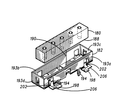
Turning now to the e~ lecl view of FIG. 5, tliçlec~ric filter
180, which is similAor in construction to ~ lectric filter 80 of FIGs 3
is ~liq~ose~l above mounting bracket 182. Filter 180 i8 of ~iimen~ions
11- 207823~
permitting insertion of the filter into mounting bracket 182 such that
bottom surface 188 of filter 180 abuts ~Pin~t a ~upport ~urface
formed within mo~.n~ing b~ et 182 when filter 180 is translated in
the direction in~licAted by arrow 190 Mounting bracket 182 includes
sidewalls 193a, 193b, 193c, and 193d.
FIG. 5 further illustrates hoQ6~1 proiect;Qn~ 194 protruding
b~DnDAtll a bollo ~ surface of the body of mounting bracket 182, foot
mem~r~ 198 e~t~n~inE~ hori7ont~11y beyond a side surface of the body
of mounting b~ ~lret 182, and strip memhers 202 formed integral with
l 0 a foot mDm~er 198 and cor~nDcte~l thereto by i~thmAl portions 206.
FIG. 6 is an overhead view of mounting bracket 182 shown in
the e~ploded view of FIG. 5. In the l,~efer.c~ emboAim~t, the
8~1ppO~ (. s~r e e of mounting bracket 182 upon which dielectric filter
180 resb in ~UIJ~O. Li~e engagement thereagainst i8 comprised of
1 5 tabular in~ent~ion~ here int3ent~;o~ 238, 240, and 242 formed of
portions of the ~idc all8 of mounting bracket 182.
In the ~.efer.od emho~iment, the suppo.l surface i8 coml,~;sed
of at least three tabular indent~tion~ as three tabular inden~ o~
define a planar surface to 8U1~PO~ l the rlieleCtric filter 180 in
2 0 sul,l,o- li~,e engagement thereagAin~t. Other numbers and other
configurations of the tabular intlent~tion~ are, of course, possihle. In
the preferred emho~limont of FIG. 6, tabular in~lerltotio -~ 238-242, as
illustrated in which tabular inden~-o-tisn~ 238 and 240 are disposed
upon sidewall 193b at opposite ends of sidewalls 193b, and tabular
2 5 indentation 242 i8 tiispose~ upon sidewall 193a at a lo~-o-tiQn
i~te. ~ o-te b~l- ee-l the positioning of tabular in~i~ont-o-tions 238 and
240 to provide tLe~ a stable suppo, l surface permitting su~- Live
engagement of a ~ottom surface of dielectric filter 180 thereagPin~t
The overhead view of FIG. 6 further illustrates spring
3 0 msmbers 244 and 248 forming leaf springs formed of portions of
~id/. ..illl8 193d and 193c es~ec~;vely. Spring members 244 and 248
esert a spring force for esertion against side surfaces of dielectric
filter 180 when inserted within mounting bracket to be supported
agPinP~t the support surface formed thereo
-12- ~07~23'1
The overhead view of FIG. 6 additionally illustrates foot
mDmhers 198 protruding beyond ~idewall 193a and two ~trip
memhers 202 integrally formed with the foot memhers 198 and
c~nect~ thereto by i~hm~ol portion 206. It is noted that strip
portions 202 include end portions 250 which, as will be noted more
fully hereinbelow, are of heightwise positions col~es~on~ing to the
heightwise position of the &U~I~Ol l ~urface ~iefine~l by tabular
in~l~ntotions 23~242.
FIG. 7 is a side, elevational view of moltnting bracket 182 of
1 0 FIGs. 5-6. The elev-o-tion~ql view of FIG. 7 better illustrates the
positioning of hQQl-q~l projection~ 194 which protrude bsn~Ath a
bottom surface of the body of mollnti~g bl e,~et 182. In the preferred
emh~lim^nt one heo~e~l projection 194 is formet integral with, and
e~tends ~neAth sidewall 193a. Two hoolre~l y~je~ :on~ 194 are
1 5 fonned integral width G~O~g sidewall 193b ant protrude beneAth
the sidewall 193b. ~oQ~e-3 projection 194 formed integral with
sidewall 193a i~ positioned interme~iAts belween the ~prce l-apart
hoQ~q-l projectir~n~ 194 formed integral with sidewall 193b. Ends of
hool~e~l project;~n~ 194 are bent to form back-~nglc i portions 194a and
2 0 194b.
Back-~ngle i portions 194a and 194b are c~p~hle of elastic
deform~tion res~bi~e to applic~ti~n of col-ly~ee~ e forces
thereP~gPin~t~ When co~l,lessive forces are no longer e~erted
thel~P~ in~t, b~ck-~ng~e~l portions 194a and 194b of hoQ~l
2 5 I,.o e ti~n~ 194 are c~pphle of re~-e~pp~na;Q~l to return to their
e positions as illustrated in the side view of FIG. 7. FIG. 7
further illw~rates ridge meml)er 256 e~n~ling laterally along
sub~tonti~lly the entire length of sidewall 193a. A ~imil~r ridge
memher is simil~rly preferably formed to e~ten~l laterally along
3 0 sl~hst~nti~lly the entire length of ~idc ~. all of 193b. Ridge memhers
256 fo~n solder surfaces for forming positive solder c~rlnectiQns with
the dielectric filter 180, as ~ill be described more fully hereinbelow.
FIG. 8 is a cutaway view of ~ ectric filter 180 positioned at the
support surface formed of mounting bracket 182. Dielectric filter 180
- 13 - 2 07823 1
and m~ nt;ng bracket 182 together form the dielectric filter Aqsçmhly
of the l,~e~.lt inV~pntion~ and referred to generally by reference
numeral 276. A_ illustrated, the bottom surface of dielectric filter
abuts ag-in~t the support surface formed of mounting bracket 182, in
S the cutaway view of FIG. 8, the bottom surface of dielectric filter 180
i8 seated again t tabular indentation 242. Mo~nting bracket 182 iQ
Affi-P~l in position upon a substrate, here printed circuit board 282. A
h~otto~^ surface of foot mPm~r 198 ç~t~An~ling horizont~ly beyond
~id~ ~. all 193a of m.^,.ln~ing bracket 182 abuts ^~inQt a top surface of
1 0 circuits board 282 to rest thereagAinat ~OQl-e'l projection 194 formed
integral with sidewall 193a and e~ten~ling therebenP~tl~ is inserted to
e~tend through an aperture 284 formed to e~t~n~l through the circuit
board 282.
Strip me-^hçr 202 formed integral with foot mPmher 198 and
l S connected thereto by iP~hm~l portion 206 includes end portion 250
which abuts agAinQt electrode 230, shown in hatch, which is formed
upon a hol~o-~. surface of dielectric filter 180. Electrode 230
~,,e~^,n-lQ to electrode 130 of dielectric filter 80 shown in the bottom
~iew of FIG. 4. A sec~AJn~l end portion, in~ t~l by refe~nca number
2 0 288 of strip me-rhsr 202 is formed to be in the same planar
configuration as that of foot memher 198 and, hence, abuts against a
top surface of circuit board 282. Electrode 230 of dielectric filter 180 is
thereby positioned in electrical connect;~s^ with circuit board 282 by
way of strip memher 202.
2 5 The enlarged, cutaway view of FIG. 9 illustrates in greater
detail strip mem~r 202. As noted hereinabove, strip m^-.^hor 202 is
formed integral with foot mpmher 198 and is ~nn-ct~l thereto by
isthmal portion 206. Strip menAbrr 202 is "s ~h~ " in . onfiguration
such that first end 250 of ~trip m-mher 202 is of an elevation
3 0 heightene l relative to secQ^d end 288 of strip m~mher 202. When
dielectric filter 180 is positioned in 8u~ live engagement agPin~t
the support surface of mounting bracket 182, and mo mt;ng bracket
182 is ~ffi~e l in position upon a substrate, such as circuit board 282 of
FIG. 8, electrode 230 of the dielectric filter 180 is mA-int-in~A i in
- 14- 207823~
electrical cQnnPction with the substrate by way of strip memhPr 202.
Ho~e~er, bPc~ e mounting bracket 182 is maintained in
electrical cQnnPcti~n with the electrically-conductive material coated
upon the surface portions of dielectric filter 180, and because strip
memhPr 202 i8 integrally formed with foot mPmher 198 which is, in
turn, formed integral with sidewall 193a of the mounting bracket 182,
the electrode 230 become~ electrically connecte~ to such electrically-
coated material coated upon the filter. Ay~.~o~.;ate application of a
solder material to desired loc~tion~ of the riielect~ic filter 180,
1 0 mounting bracket 182, strip m~mher 202, and circuit board 282 of
FIG. 8 and h?^t;ng of the rlielectric filter ~ssqmhly 276 together with
t_e printed circuit board 282 (or other substrate upon which the
ml~llnting bracket 182 ig mounted) according to a coll~eJ tional reflow
solder t~hnique forms solder connec~ionR at the desired locAti~n~ to
1 5 affis, and to electrically interconnect the desired portions of ~lielect~ic
filter 180 to the circuit board 282.
To elect~ically isolate the electrode 230 of filter 180 from such
electrically-coated material once the filter is positioned in ~ live
engagement upon the support surface formed of the mounting
2 0 bracket 182, isthm~l portion 206 i~ cut, or otherwise ~evered, along a
line in~ te~ by X-markings 294.
Elect~rode 230 is m~int~ine~l in the electrical connection with
the circuit board 282 by way of strip member 202, but is electrically
isol~t~ from other surface portions of the dielectric filter 180 and
2 5 I-,OUUti~ bracket 182.
The enlarged, cutaway view of FIG. 10a illustrates the
po~iti~ning of mo~lnting bracket 282 and hoQ~e-l projection 194 during
insertion of the hooked projection 194 through an aperture 284 formed
to e~tend through circuit board 282. A~,erl,~a 284 is of dimenRiQn~
3 0 such that insertion of h~Q~e~l projection 194 therein is permitted, but
co~lessive forces are exerted against back-angled portions 194a and
194b ofthe hooked projection 194. Fl~t;c deform~t;~n permitted of
the back-angled portions 194a and 194b c~ by the e~ertion of the
compressive forces thereupon permits tr~n~lAtiQ~ of the hooked
207~234
y~O aC~;?n 194 through al,erl u~e 284.
FIG. 10b is an enlarget, cutaway view, similQr to that of FIG.
10a but wherein mounting bracket 182 is QffisP i in position upon
cimut board 282. Hooked projection 194 i8 of a length such that,
S when a bottom surface of mounting b~ et 182 abuts against a top
surface of circuit board 282, back-angled portions 194a and 194b
çs~n-l at or beyond the hott~m surface of circuit board 282.
Co,uy.~t_:~e forces eserted ~in~t the portions 194a and 194b by
sidewalls ~1 ~finin~ aye~ o 284 are no longer eserted. Because of the
1 0 çl~;~ty of the back-Qngle i por ions 194a and 194b, re-espQnRiQn of
the portions 194a and 194b occurs, and the ~iiQmPtrical rlim.~?n~iQn
across back-Q~e~l portions 194a and 194b eS~ee~ls that of the
diameter of a~, ~u~e 284. TrQn~lQti~n of the h~l-~ p,oj~ion 194 out
of a~. lu~e 284 is ~.e~t -.ted, and mQ~nt;ng bracket 182 is thereby
Qffi~e~ in position upon circuit boards 282.
Turnin~ now to the flow diagram of FIG. 11, the me~l~l steps
of the me'llo~l for mounting a tiiPlect-ic filter upon a substrate of the
.ea&.lt ill~ lion are listed. First, and as in~licQte i by block 310, a
support surface is formed upon the substrate to auy~ the dielectric
2 0 filter in 8~ ive engagement thereat. Ne~t, and as in~liCQ~l by
block 314, portions of the ~liçlect~ic filter are electrically co- n~cte~l to a
desired portion of the substrate. Nest, and as inAic~t~l by block 318,
the portions of the fiielec~ic filter electrically c~nnecte~ to the desired
portion of the substrate is electrically i~ol~te~l thelef~
2 5 As mentioned hereinabove, the su~l l surface is formed of
t~e mc ml~;ng bracket, and, as illustrated in the preferred
~m~iment of FIGs. 5-8, the su~,oll surface is comt,.;sed of tabular
indentation~ formed of portions of the sidewalls of the mounting
bracket to pe.~t se~t;ng of the ~lielec~ic filter in ~U~IJOl l.ive
3 0 engagement thereag~in~t. Strip m ~mhers of electrically-conductive
matenal formed integral with the mounting bracket, and as
illustrated in the ~rcfel-ed PmhoAiment of FIGs. 5 9, interco~nect the
portions of the dielectric filter (in the ~ Efer.ed embo~iment~ the
electrodes fonned thereupon), and the substrate. In the preferred
- 16- 2078~34
emho~lim^--t, more particularly, the substrate comprises a circuit
board upon which an electrical circuit i~ disposed.
A reflow solder technique may be advantageously lltili7~ to
form a solder cQ~nec~;on between the strip memhPrs and the
S dielectric filter and between the strip m~Pmhers and the substrate.
Because formation of the solder conn--~iQ~ by a reflow solder
technique does not result in formation of large amounts of solder
flu~, the need to remove such solder flus by application of a freon
(tm~based material (conventionally required when solder
conn ~;on~ are formed by immersion of a substrate into a molten,
solder bath) is obviated.
Once solder conn~ctisn~ have been formed, the portions of the
.lielec~-;c filter (i.e., in the t,iefe.,ed emho~limpn~ the cle_l,odes
formed thereupon) conn~ te~l to the desired portion of the substrate is
1 5 electrically i~ol~te~l from the 8~ 1, surface formed of the ~lnting
bracket by sevenng, by c~t~;ng or otherwise, of the strip me~rs
from the m~ lnt;ng b, -lret.
The liPle~ic filter and mounting bracket of the present
invention may be advantageously utilized to form a filter for a two-
2 0 way radio, such as a radiotelephone. The r~tiiotelephnrle may, for
P~mple, be ~imil~r to the tran~ceiver shown and described in
Motorola instruction m~nll~l mlmhPr 68P8107E40, and entitl~
"DYNATAC Cellular Mohile Telephone" p-lhli~he 1 by Motorola C&E
Parts, 1313 East Algonquin Road, Schaumburg, 111. 60196.
2 5 FIG. 12 i8 a block diagram of a two-way radio simil~r to such
radiotelephone, and is in~lic~te~l~ generally, by ~efele.lce numeral
400. Radiotelephone 400 may, for e~mple~ co~ ,r;se a
r~A;~te!ephone ~ ed in a cellular, commllnic~;on system. A
signal transmittet upon a radio frequency ch~nr?~ is received by
3 o ~ntqnn~ 406, which, ~lhse~Uent to ~c~ption, i8 supplied to filter 412
on line 418. Filter 412 filters the received ~ignal and generates a
filtered signal on line 418. Filter 412 may be formed of a dielectric
filter ant mounted upon a circuit board by a mounting bracket as
described with ~e8~1 to FIGs. 3-11 hereinabove.
- l7 - 2078~34-
T ine 418 ig coupled to mixer 424 which also receives an
os~llot;nig signali on line 430 formed by frequency srtl esi7~ 438
l~g~o~s*e to the os~ nL7 frequency of lefe~ence osrill-o-t~r 446, the
08rillotinjg gigna]i generated thereat being cQnnecte~l to synt~ e~i7er
438 on line 452. ~ser 424 co"~e, ls downward in frequency the signal
sllpplie~ thereto on line 418, and generates a down~iull~e, led signal
on line 458 which is supplied to filter 464. Filter 464 generates a
filtered signal on line 472 which is sllpplio~l to secon~l miser 680.
Filter 464 may also be formed of a flia~ ic filter and mn~lnt~l upon
1 0 a circuit b~ard by a mounting b.ac~et as described with ra~lp4ct to
FIGs. 3-11 hereinabo~e.
Miser 480 additionally r~ceiveg an os~illot;ng input on line 686
gllppli~ by og~ tQr 492. The os~llst;nig frequency of os~ l-o~tQr 492
is controlled by the os~ll-o-t;nig frequency of reference osrill~tQr 446
1 5 and is co~lple 1 to osrill~tQr 446 on line 498. Mi~er 480 generates a
second, down cG"verled signal on Une 504 whichi is suppUed to the
demodulator circuit 510. Thie ~^mo~llll-o-tQr circuit 510 generates a
demo~ o-te~ signal on line 512 which is supplied to a transducer,
such as spe-o-lrer 524. ~peo-l~er 524 CO~ el 18 the signal PllpF~ thereto
2 0 into an All~ihle ~ignol
A transmit portion of radiotelephone 400 includes a transducer
such as microphone 530 which co.l~ells a voice signal into electrical
form and generates a signal in~iic~1;ve thereof on line 536. Line 536 is
coupled to m~lllotQr 542 which cO~I~el 1,8 the electrical signal
2 5 supplied thereto into a modulated form. Whilê not shown, modulator
542 includes .~ circuitry, l,r~ferably coupled to reference
oscillator 446, for generating a ml~A~ t~ i signal on line 560. I~ine 560
i8 coupled to Slter 570, which also may be formed of a lip~lec~ric filter
and mounted upon a circuit board by a m~lnt;ng bracket as
3 0 described with l~b~,e.,l to FIGs. 3-11 hereinabove. Filters 412 and 570
may together form a duples filter with a~l,loy.;ate nllm~r of, and
posit;sning of, electrically-conductive strip m^-nhers. A filtered
signal generated by filter 570 i~ coupled to ont~nno 406 by line 580.
The Uock diagram of FIG. 12 illu~tratês but one circuit of which the
- 18- 207~34
~ic filter ant mounting bracket of the present invention may
form a portion. The ~liPlect-ic filter and mounting b~ ?~l~et of the
~i~fer-~d ~mhoAim~nt of FIGs. 3-10 m ay, of course, be
advantageously ~ i7e-l to form portions of other electrical circuits.
S While the present invention has been described in cor nec~ion
with the l~refe~ed çmho~liment~ shown in the various figures, it is to
be understood that other simil~r emho~iiment~ _ay be used and
motlific~1;on~ and ~r3~ )n~ _ ay be m ade to the described
Pmho~iiment~ for perfo~ing the same filn~;or of the ~cee,lt
invention without deviating the~efio~ The~efo~e, the plcee.lt
in~e,l~on should not be limited to any single çmbQA;~ nt~ but rather
construet in b~ t~ and scope in accordance with the recitation of
the appended ClQimQ