Note: Descriptions are shown in the official language in which they were submitted.
`WO 92/134;!5 2 ~? 7 ~ PCr/GB92/00143
NON-SKARP CUT FILTERS FOR ASSEXBLING AND SPLI~TING I~'
WESTON CLEAN PAL
FIELD OF l~E: INTrENTION
This invention relates to the ~eston PAL video signal
(W-PAL), and in particular to improvements in the assenoler and
splitter which respectively, assemole and split luminance Y and
chrominance (U+V/U-V) components.
BACRGROUND TO T~ rNvENTIoN
The Weston Clean PAL system is described in GB
1534268 to 1534270 and in ~BC ResearcA Department Report No: ~
Ig80/1. The contents of these four documents are incorporated -
Aerein by reference. W-PAL obtains separation of luminance and
chrominance by phase segregation, whereby the luminance is sampled
at a frequency of twice the colour subcarrier frequency thereby
causing it to appear as double sideband modulation of the colour
subcarrier. At the same time the two chrominance components are
formed into a single signal consisting of the quantities (U + V)/J2
and (U - VJ~.'2 on alternate lines which modulates the subcarrier
directly. If PAL compatibility were not required the two
modulation processes could be in quadrature so enabling the
subcarrier to carry both luminance and chrominance without
interaction in spite of their occupying the same spectral space.
Fig. l shows the two-dimensional spectrum of the alternate-line
chrominance and the sampled luminance, from which it can be seen
that there is a considerable overlap of the luminance and
chrominance spectra, amounting to the region 3.36 - 5.5 ~Hz in
system I PAL. This region is the region in which aliasing will
occur at 2 Fsc sampling (8.86 MHz - 5.5 MXz = 3.36 MHz) and varies
with different PAL standards.
Compatibility with normal PAL, however, requires that
the signals are further processed before com~ination. In
W O 92/13425 2 0 7 ~ ~ ~ ~ PCT/GB92/00143
particular, the combined chrominance signal must be phase shifted
so that spectral components at 3~4 line offsets are in phase
quadrature with components at 1/4 line o~fsets, restoring the phase
quadrature between U and v. This must be done in such a way as to
preserve the potentia~ phase separation between chrominance and
Iuminance. At the receiver, the W phase separation is removed and
the luminance and chrominance are separa~ed by synchronous
demodulation. These complex functions are provided by so-called
assembler and splitter circuits which lie at the core of the ~eston
Clean PAL system. These circuits are described in GB 1534Z68 -
1534270.
S~MMARY OF T~E INVENTION
The present invention aims to provide an improved
ass~mbler and splitter through improved filter desisn.
We have appreciated that cross colour effects may be
eliminated without affecting the luminance bandwidth and
independently of the link filter in the PAL transmission channel.
This may be achieved by ensuring that filters in the W-PAL
assembler and splitter have the correct interrelationship.
~ e have appreciated that the filter in the luminance
channel of the splitter must have an amplitude which is a shifted
mirror of the filter in the chrominance path of the assemoler.
Moreover, the filter in the chrominance path of the splitter must
have an amplitude which is a shifted mirror of the amplitude of the
filter in the luminance path of the assembler. Furthermore, the
product of the filters in the luminance paths in the assembler and
splitter must be a Nyquist filter. Similarly, the product of the
filters in the chrominance path OI the asse~oler and splitter must
also be a Nyquist filter.
The phase of the luminance and chrominance filters in
-the splitter may be the anti-mirror of the phase of the chrominance
and luminance filters respectively in the assembler.
Preferably, the filter in the luminance channel of
- .
--~~ W 0 92/13425 2 ~ 7 ~ 3 ~ PCT/GB92/0~1~3
-- 3 --
the asse~oler e~tinguishes below the frec~uency or the link filter
in the PAL channel. This means that variations in link bandwidth
affect the horisontal chrominance bandwidth only and not the
ability to eliminate cross colour effects or the luminance
bandwidth.
The invention is set out in the indepenàent claims to
wnich reference should be made.
Various modifications, further improvements and
preferred features are set out in the deDendent claims.
DESCRIPTION OF DRAWINGS
An embodiment of the invention will now be described
with reference to the drawings in which:
Fiaure 1 shows the two dimensional spectrum of . ~;
sampled luminance and line alternating chrominance modulated on the
subcarrier and showing spectral overlap;
Fiqure Z shows, in block form, the components of a
conventional Weston Clean PAL assem~ler and splitter;
Fiqure 3 shows the generic circuit form of the
circuit of Figure 2;
Ficure 4 a) and b) shows the amplitudes of the
frequency characteristics of the functions Fl and F2 of Figure 3 in
the known system shown in Figure 2;
Fiqure 5 a) and b) show e~amples of the amplitudes of
the frequency characteristics of the functions Fl and F2
respectively of Figure 3 embodying the invention;
Fiqure 6 a) and b) show e~amples of the amplitudes of
the frequency characteristics of the functions Fl and F2
respectively of Figure 3 also second embodying the invention.
Fiqure 7 a3 to d) show circuit realisations of the
proposed transfer functions for Fl, F2, F3 and F4 in Figure 3,
- embodying the invention; and
.. . . , . : . :. ... . . ~
W O 92/13425 2 V 7 ~ ~ 3 ~ PCT/GB92/00143 ~-
Fi~ure 8 a) and bl shows improvements to Figure 7 in
which functions F~ and F2 and F3 and F4 are continued to reduce the
number of components required.
The assembler and sDlitter used by the origina1
~eston Clean PAL system are shown for convenience in Fig. 7. This
circuit accepts lu~inance sampled at twice the subcarrier frequency
and combined chrominance modulated on the subcarrier, in phase with
the sampling. Synchronous sampling of the luminance output and
cophased demodulation of the chrominance output yield signals
without cros~-effects. As can be seen, both sending and receiving
networks are characterised Dy a single band-pass filter lO0 wAich
defines the region of luminance/chrominance spectral overlap
together with a line delay which helps to form a comb filter in
this region. The low-pass filter llO is needed to ensure correct
luminance perirormance and is assumed to occur on the link betw~en
sender and receiver. The transfer functions for the luminance to
PAL and PAL to luminance paths are not ide~tical since, at the
sender, the low frequencies are undelayed whereas, at the receiver,
they are delayed by one line. This equalises the delay in the
overlap region which is half a line at both ends. For a fuller
description of the assembler and splitter reference should be made
to Figure 6 of GB 1534268 to 153427a.
The generic form of the assembler and s?litter is
shown in Fig. 3 which defines filter functions F~, F2, F3 and F4.
In the above case the input and output carriers are cophased, as
previously mentioned. The filter functions for Fig. 2 then become
F, = L ~l + B(z-l - l)j2
F2 = LE(l - z-l)j2
F3 = z-~ I B(l - z-l)j2
F~ = B(z-l - 1)j2
. - - . , ~ . , :
.
~W O 92tl3425 2 ~ . 3 rJ PCT/GB92/00143
where z-l is the transfer function of a line delay, i.e.
Z- l = ex~ g )
where
~ = 2~fT.
::
and L and B are the transfer functions of the low- and band-pass
filters respectively. The amplitudes of the frequency
characteristics of F and F2, remembering that they are complex,
are shown in Fig. 4. That of F4 is identical to that of F2 whilst
that of F3 is similar to that of Fl without the upper band limit.
The use of a band-pass filter in combination with a
low-pass filter is bad practice since two filters define the upper
edge of the signal. This is an historical hangover from the
original hardware implementation of the system in which the
band-pass filter worked at a sampling frequency of 2f.c as
descri~ed in GB I~3~268 and ~BC Research Department Rep~rt No:
1~76~24. The theory of the original system assumed that the
filters were of infinitely sharp cut so that this did not matter.
The objection can be answered by replacing the band-pass filter
with a high-pass filter.
Perfect phase segregation, however, still appears to
require filters with an infinitely sharp cut. Practical filters
have a finite rate of cut and so the phase segregation will
potentially fail at the edges of the overlap band in the transition
regions of the low- and high-pass filters. This undermines the
case for phase segregation since it is based on the proposition
that lumi~ance-chrominance separation does not depend on sharp cut
filters as it does with band-segregation. (In mitigation, the
failure is with horizontal filters which can be made sharper than
vertical or temporal filtersl. It is therefore of crucial
importance to discover if this requirement for sharp cut filters is
fundamental. Experience with filtering for sub-Nyquist PAL,
samDled at 2fnc, suggests that this may not be so.
W O 92/1342S
2 ~ 7 8 ~ 7.~ PCr/GB92/00143 ~
It has been shown that the general requirements on
the Iilters Fl, F2, F~ arld F4, if the carriers are cophased, are
given by
FlF3 = Ny
F2F4 = Nc
FlF4 = jSYc
F2F3 = jSCY
where N is any skew-symmetric function and S is any sy~metric
function about the carrier frequency, that is,
.
N(f) = l - N~(Zf~c - f)
and
S(f) = S~(2f~c - f)
remembering that N and S can be comple~. This condition for N
makes it a so-called Nyquist filter. If these conditions are
obeyed then the pure imaginary cross transfer functions put the
unwanted signals in quadrature with the demodulating sinewaves in
both cases whilst the transfer functions for the wanted signals are
flat through the complementary sideband principle.
Now, considering the transfer functions of the
original systems with perfect filters, the wanted and cross
characteristics within the combing region, where B and L are unity,
are given by
:
FY = FlF3 = ~(1 + 2Z-1 + z-2)
~Z ( 1 + COS ~3 ) '
Fc = FzF4 = ~(-l + 2z-l - z-Z)
~z-l(l - COS ~)
FYC = F.F4 = ~(z-z - ;) -
= -~z-ljsin 6
FCY = FzF3 = ~(l - z- )
= ~z~Ljsin 6
- .. .. . .. .
,- W O 92/13425 ~ ~ 7 ~ '7 3 '3 PCT/GB92/00143
As ~ has the value 3n/2 at f~c it is clear that, within the combing
region, the transfer functions OI the wanted signals are
skew-symmetric whilst those of the cross signals are symmetr.c.
.hus we may write
rY = z-lN
Fc = z-lN2
FYC = ~ S ::.
FC~ = Z-IjS
wAer_
' ''
.;L = ~(1 + COS ~) . .
~ = ~(1 - cos ~) '
S = ~sin
As the combing region is s~mmetrical about f~c it follows tha. FY
is stilI skew-symmetric outside it since FY rises to unity below it
and drops to zero beyond it. However, at the edges of the com~ing
region, it is stiII possible for its skew symmetry to hold if the
shapes of the upper and lower edges obey the condition since the
contents of the envelope already obey the condition. ~owever,
ia clear that this situation does not apply to Fc since F2 and F4
are ~ero on both sides of the combining region and therefore also
YC and FCY. But it dces suggest that a solution might be possible -
if F2 and F4 are allowed to remain at unity at one end of the
combing region witA conditions cn the upper and lower edges.
Consider amplitude transfer functions for F1 and F- -.
as shown in Fig. 5 with those for F3 and r4 being identical. FL iS
now characterised by two low-pass filters, Ll and L2, which deiine
the lower and upper edges of the combing region whilst F2 is
characterised by two high-pass filters, Hl and ~, which do the
same for the chrominance. , Note that F2 continues at unity
indefinitely as the freguency rises.
.
:
- .. ,. . ~ . . .. ~ : ,... , . . : . . ,. , , ,- .-, . :., . . :. .
W O 92/1342~ PC~/GB92/00143
~ aking into account the need for equalising .he delay
oetween low and high frequencies, let the transrer functions be
Fl = L1 + tL2 - L1)~1 ~ Z~ 'Z
F2 - H2z-l + (H1 - h'-3(z-l - l1i~
r3 = Llz-l + (L2 - Ll)(l ~ Z~
F4 = H2 + (~l - H2)(1 - z-l),'2
Then, aiter some algebraic mar.i2ulation, the wanted and cross
transfer functions are given by
Fy = ~-I[L22Nl . Ll2N.j
Fc = z-l[H22Nl + HlZN2]
Frc = z-l~L2H2Nl - L~HlN2 + j(LlH- ~ L2n1)S~
FCY = Z-1[L2H2NI - LlHlN2 - j(LlH- ~ L2H.)S3
.
~Aere NL, N2 and S are th~ transfer functions of the nideal~ system
in the combing region, as defined above.
Where the filters Ll, L2, ~l and H2 are sharp cut,
these equations reduce to those above except that FYC and FCY are
reversed in sign. Thus, in FY at low frequencies, where both L
and L2 are ur.ity, the function Nl + N2 is also unity and similarl~
for Fc a' high frequencies. In Frc and Fc~, 'he func'ions LlH1 and
L2Hz are zero since they are products of coincident infinitely
sharp rising and falling edges. Meanwhile, the function Lln2
L2Hl corresponds to a bandpass filter because the firs. term is
zero as Ll and H2 do not overlap. ~ , -
In a practical situation where the filters are not
sharp cut we can impose the requiremecnts for sxew symmetry to yield
conditions on the filters. For FY we have, substituting for Nl, 1~2
and S:
'!f)+Ll2(f)+~L22tf)-Ll (fl3cos a + L2'(2~c---) ~ LL2~2f~ - f)
!L22(2f~ - f) - Ll2(2f~ - f)3cos (Z6~ - a) = 2
,, ~
- ~ . .`X ' '' .
W O 92/134~S 2 Q 7 ~ ~ PCT/GB92/00143
g _ ~;
wnere
6~C = ZrtI.:~rL
3~ 2
Substituting for 68C and equatin~ powers of cos ~ we have
L22(f) ~ Ll2(f) + L22(2f~c - f) + Ll2(2f~c - f) = 7 ':
and
L2-(fl - ~lZ(f) - L22(2.-~c _ r) + Ll2(2f~c - f) = 0
which leads ~o
L2Z~f) + Ll2(2'~c - f)
~Aich means tha. L1Z is the complemenl of the charact2risti. of L,- `
reflectea about the frequency f9c.
în the same way, for Fc we Aave
H2:(fl+Hl2(f)+[H27(f)-Hl2(f)~cos a + H2 (2f~;c-f)+H~2(2f~c-fl -
+ [H22(2f~c - f) - H.2(2f,c - f)~cos (2acc - 6) = 2
Substitutins f~r ~c and equating oowers of cos ~ we have
H22(f) ~ Hl2(f) + H22(2f.c - f) + Hl2(2`~ - f) = 2
and
h'-'(f) - h'l2(f) - H22(2f~c - f) i HlZ(2f~c - .^) = 0
wAich leads to - -
H22(f) + hl2!2f~c - f)
which means that H1Z is the complement OI the characteristic oi H2Z
reflected about the frequency f~c.
~urning to FYC and FCY however, it is clear that the
original conditions cannot be satisfied because, in addition to the -
pure imaginar-~ term, there is also a real term which is non-zers
when the filters are not sharp cut. All is not lost, however,
since i. is possible to have
Fyc = z-l[A ~ jS
.. . . . . , ,i .... ;.. . ,.. , ,~,, :: ,., ,; , : . ,"" .. ... . .
W O 92/1342~ 2 B 7 ~ ~ 3 ~ PCT/GB92/00143 ~
.
where A is truly antisvmmetrical about the subcarrier frequency,
i.e.
~(f3 = -A~(2fcc - f1
since, upon demodulation, eacA frequency component o~ the upper
sideband is cancelled by the corresponding lower sideband component
of a signal undergoing the .ransfer function A.
Imi~osing the antisymmetry condition on tAe real part:
L2(f]H2(f3 - Ll(-)hL~f) i ~2(f)h2(f) I Ll(f)Hl(f)1cos
L-(Zf~c - f)H2~2f~ - ~) - ;l(2f.c - f3Hl(2f~c - f)
i[~2(Zfcc - f)H2(2fc~ - f)
+ Ll (Zfcc - f )Hl (2fcc~f ) ~cOs(2~cc - ~ ) = O
Subst:tuting for a.C and equating powers of cos a we have
L2!f~H2(f) - Ll(flH~tf)
+ L2(2f~c - f)H2(2f8c - f 1 - L~(2f~c - f)H (Zf~c - f) - 0
and
L2(f)H2(f) + Ll(f)Hl(f)
- L2(2fcc - f)H2(2f~c - ') - L,(2fcc - f1Hl(Zfcc - f) = 0
which leads to
L2(f)Hz(f! - Ll(Zfcc - f,h-l(2f~c - f) = 0
Substituting for Ll and Hl in terms of L2 and H2, as derived above,
gives
,:,
L2(-3H2(f, = .[l - L22(f)~ l - H2Z(f)1
which, after some algebraic manipulation, gives
L2Z(f ) + H2Z(f ) = ~. ,
and hence
Ll2(f) + Hl~(f)
. ,.. . . . - , .
- - . . .
~: ~ - ? ~`
~,, .
~ ~ 7 1~ x 3 nJ
~'~W O 92/13425 PCT/GB92/OOt43
or
;.(2f=c - f) = ~2 ( ' !
and
~(2f8c - f) = n~(f) `~
sAo~ing that K2 is the reflection of L1 about f~c whilst Hl is the
reflection of L2 about fcc and also that Hl is square root
complementary to Ll wnilst H2 is square root complementary to L2.
This latter means that Hl and H- cannot be obtained from Ll and L2
by simple subtraction.
~ mposing the symmetrv condition on tAe pure i.~aginar
par.:
[~l~f)H2(f) i L2(f)Hl(f)~sin 6
[L~(2- c-flH2(2fcc-f) i Lz(2f~c - f)Hl(2 ~c - f)3sin t26~c - ~l
Substituting for a.c we have
sin (2a~c - a ) - sin
and
Ll(f)K2(L) ~ L2~f)Hl(f) =
L~(2f8c - f)H2(2f~c - f) ~ L2(2f8c ~ )ff~(2fcc - f)
.igain, this can be satisfied by
:
L2(2f~c - f) = Hl(f~
and
L~(2f~c - f) = K2(i)
sAowing tAat the above result is consistent.
The relationship derived between L2 and ~l and ;
between Ll and ~2 means that F4 is, in fact, the shifted version Ot
F. and F3 is the shifted version of F- (actually the negative),
tha. is
~ 0 ? ~ ~ 3 ::
W O 92/1342~ PCT/GB92/00143
- 12 -
F~(.) = Fl(f - 2f~c)
= F,~2f~c -
and
r3(.1 = -r2(f - 2f~c;
2~(_f~c - -
since
z-~( - 2f~c) = _3-l(f)
It is these facts which help to give F~F~ and F2F3 the special
properties. I~'ote that this would not be so if F2 and F4 were
interchanged. But they could be if F~ and F3 were also
interchangec.
~ he derived relationships show that cnce one or the
filters Ll, L2, H~ and H2 is specified i~ sets the others. Phase
segregation imposes no restriction on the form of the specified
filter but the form does govern the nature of the compatibility of
the assembled PAL signal with conventional PAL. If we choose to
specify L2 then this means that phase segregation would allow its
transition band to lie, for example, anywhere in the original
combing region between 3.3 ~Hz and 5.5 MHz but compatibility would
require it to start at or beyond f~c so that the PAL signal is
compa~ible in uniform-coloured areas. For example, Fig. 5 shows a
characteristic which starts at f~c and s~ops at 5.5 I~HZ and is the
square root of a linear decrease whilst Fig. 6 shows a sharper
characteristic which starts at fcc and stops at 5 L~Hz. In such a
case the signal beyond the combing region is the line-alternating U
+ V, U - V chrominance signal modulated on the subcarrier.
One conse~uence of this is that it can be arranged
that the characteristic of L2 is extinguisAed at a fre~uency which
is below the cut fre~uency of any filter which exists on the PAL
link such as might be expected in, for example, a transmitter.
~hen the properties Fy~ FYC and FCY are not dependent on such an
exlernal filter which onlylaffects the property rC. In other
words, band limiting the PAL signal af~ects only the chrominance
bandwidth and not the luminance bandwidth or the pnase segregation.
. . - , . . - . - - ~
- ~0~3`,i
~~ W O 92~1342~ PCT/GB92/00143
- This is extremely important, especially in the context of differins
PAL systems. For e~ample, the charactexistics of Fig. 6 wil! be
compatible with both systems I and B/G.
~ o obtain circui. realisations of the transfer
functions F~, F2, F3 and F~ whicA are balanced the equations may be
rearranged as
F~ 2 + Ll)~2 + (L2 - L~J z-1~2
F = -(Hl - ~_)f2 ~ (~1 + H2) z-lj2
F3 = (L2 - ~.L);2 i (L2 + L~) z-~/2
r~ - (hl i ~:2)jZ - (Hl - ~2) ~-lf2
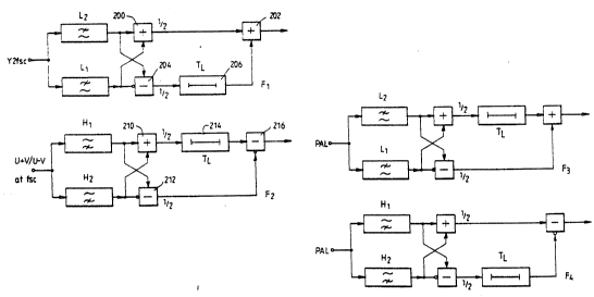
Fig. 7 a) to d) shows the c rcuits of these
realisations. '-
rn Figure 7 a) the input 2 Fsc luminance component is
filtered in parallel low pass filters Ll, L2. The output from each
filter is summed by half adder 200 whose output (Ll, + L2)f2 forms
an input to adder 202. A half subtractor 204 has an input from
filter L2 and an inverted input from filter Ll giving an output tL2
- L~)f2. This output is delayed by one video line by line delay
206 as required by the ~eston P~L system (see
Figure 2) and forms the second input to adder 202 . The output from
adder 202 forms one input to the adder shown in the generic circuit
diagram of Figure 3. The other input is provided by the circuit of
Figure 7 b) which operates on the Fsc U+VfU-V chrominance signal.
The circuit is similar to that of
Figure 7 a) but the low pass filters are replaced by high pass
filters Hl, ~2 and the output from the hal~ adder 210, rather than
the half subtractor Z12, is delayed by video line delay 214.
Subtractor 216 provides tAe second input to the adder of the
generic circuit. --
Figure 7 c) operates cn the PAL luminance component
and its frequency characte,ristic is a shifted version of the filter ~-
WO 92/1342S ~ 0 7 ~
PCT/GB92/00143
of ~igure 7 b). Figure 7 d) has a frequency characteristic which
is a shifted version of Figure 7 a). The relationship between
these filters was discussed earlier.
Figure 8 a) shows how Figures 7 a) and 7 b) may be
combined to eliminate a video line delay. In this figure the low
and high pass filters and half adders correspond to the similarly
positioned components in Figures 7 a) and b). Adder Z20 sums the
output of half subtractor 204 in the low pass section and half
adder 210 in the high pass section and provides the input to line
delay Z22. Subtractor 224 subtracts the output of half subtractor
212 c the high pass section -rom the output of hal~ adder 200 ln
'he iow pass section. ~he final adder 226 corresponàs to the adde~
in the F~gure i generic circuit and has a W-PAL output.
Figure 8 b) shows a similar combination of figures 7
c) and
7 d) whic5 reduces the number of adders and subtractors requires
and uses a single line delay 230. The filters Ll, Lz, Hl, H2 are
replaced by filters L2 t Ll , L-_- Ll , Hl - H2 and
2 2 2
Hl t h2.
The description has been given in the context of
system I PAL which has a bandwidth of 5.5 Mhz. The assembler and
splitter are equally applicable to PAL standards such as system B,
G PAL with suitable variations in filter cut frequencies.
The description has described all components in terms
of hardware. Many may be implemented in software.
.
:: ,