Note: Descriptions are shown in the official language in which they were submitted.
2 ~ 7 ~
SPECIFICATION
Title of the Invention
SUPERCONDUCTING THIN FILM FORMED OP OXIDE
SUPERC(:INDUCTOR MATERIAL, SUPEl~CONDUCTING
DEVICF, UTILIZING THE SUPERCONDUCTING THIN
PILM AND METHOD FOR MANUF~CTURING THEREO~
Background of the ~vention
Field of the invention
The present invention relates to a supereonducting thin ~llm, a
superconducting device and a method for manufacturing thereof, and
more speci~lcally to a superconducting th;n fiIm ~ormed of an oxide
materia}, which has an oxide layer improving ~quality of the
superconductin~ thin film, a superconducting device utilizing the
superconducting thin film alld a method for manufacturing thereof.
Description of related art
FundamentaI deYices which utilize superconductivity operate at a
higher speed and/or lower power consump~ion so that they will have ~r
better performance compared with those of semiconductor de-~ices. The
oxide superconductor materia3s which have been recently advaneed in
study make it possible to prepare supercQnducting devices whic~ operate
at relatively high temperature.
Superconducting devices have superconducting parts such as
supcrconducting electrodes, superconducting channels, etc. These
superconducting parts are usually forrned of superconduc~ing thir~ films.
- :, ~ , ~,
, ~ , - - ,
:,~: ;
2~78~0
In order to prepare the superconducting parts, it is necessary to finely
process supe~onducting thin films in order to obtain extremely fine
structures. ~ this connection, it is desirable that the superconducting thin
film has an ultra thin thickness.
An oxide superconductor has a layer-ed crystal structure and it is
possible to stack in order each layer of the oxide superconductor crystal
by an MBE3 (mo~ecular beam epitaxy) process so as to form a c~ystalline
oxide superconductor thin ~ilm. Therefore, it is also possible to ~o~n a
crystalIine oxide superconductor thin film in which crystalline lattices are
disposed to constitute one unit-cell layer by an MBE process.
However, superconducting current does not flow in the crystalline
oxide superconductor thin film of one unit-cell, there~ore it is necessary
to stack at least two unit-cells of crystalline lattices to form an oxide
superconductor thin film in which superconducting cuIrent flows.
Summary of the Invention
Accordingly, it is an object of the present invention to provide a
crystalline oxide superconductor thin film in which crystalline Iattices are
disposed to consti~ute one unit-cell layer, which have overcome ~e above
mentioned defects of the conventional ones.
Another object of the present invention is to provide a
superconducting device which utilizes the crystalline oxide
superconductor, which have overcome the above mentioned de~ects of the
conventional ones.
Still another object of the present invention is to provide a met~od
for manu~acturing an oxide superconduGtor thin film which have
overcome ~e above mentioned defects of the conventional ones.
:
.
- ...... ~ . :
The above and other objects of the present invention are achieved in
accordance with the present invention by a superconductin~ Ihin film
folmed on a substrate, comprising at least one oxide superconductor l~yer
formed on the principaI surface of said substrate ~nd at least one oxide
layer :formed of an oxide which improves at mos~ surface of said oxide
superconductor ~ayer, and which is arranged on or under the
superconducting layer.
The oxide superconductor layer of the superconducting thin film in
accordance with the present invention may be composed of the oxide
superconductor crystal layer in which one unit-cell of crystalline lattices
are disposed.
In a preferred embodiment, the superconducting thin film in
accordance with the present invention comprises multiple oxide
supercond~ctor layers formed of an oxide superconductor and multiple
oxide layers formed of said oxide, which are stacked alternately. Of
course, the oxide superconductor layers may be composed of ~e oxide
superconductor c2ystal layers in which one unit-cell of crys~al3ine Iattices
are disposed.
The oxide layer of the superconducting thin film in accordance with
the present invention is preferably connposed of Ba(: uO2 or
PrlBa2Cu3C)7 . In this connection, the oxide layer is composed of a
complete crystalline BaCuO2 layer or a compIete crystalline
PrlBa2Cu307 ~ layer.
These o~ide layers compensats ~or crystalline incompleteness of
both on an upper surface and/or on a bottom surface of an oxide
superconductor layer.
- 3 -
2 ~ 7 ~
Therefore, lat~ice order on the upper or the bottom surfaces of the
extremely thin oxide superconductor layer of ~e superconducting ~hin
~ilm in accordance with the pre~ent in~ention can be complete enou~h to
conduct the superconducting current e~en if the 01~ide superconductor
layer is composed of the oxide superconductor crystal layer in which only
one unit-cell of crystalline lattices are disposed.
Therefore, it is possible to control carrier density of the
superconducting thin film in accordance with the present invention by
changing the number of the superconductor layers which are included
arnong the whole ~llm t~ickness.
For this purpose, the oxide layers are pre~erably composed of high
crystallinity in which one to five unit-cells of crystalline lattices are
stacked~ The oxide layer which is composed of the incomplete crystal
lattices does not have this effect~
According to another aspect of the present invention, there is
provided a superconducting device comprising a substrate, an extremely
thin superconductiIIg channel formed on the principal surface of the
substrate, a superconducting source electrode and a superconductirlg drain
electrode of a relatively thick thickness formed of the o~ide
superconductor at the both side of the superconducting channel separated
~rom each other but electrically connected through the superconducting
channel, so that a superconducting current can flow through the
superconducting channel between the superconducting source electrode
and the superconducting d~in elec~rode, and a gate electrode through a
gate insulator on ~he supercondusting channel ~r controllillg the
superconducting current flowing through the superconduc~ing channel, in
which superconducting channel is composed of a superconduc~ing film
.
2~7~
which comprises multiple oxide superconductor layers formed of an oxide
superconductor and multiple oxide layers formed of an oxide which
improves at most surface of said oxide superconductor laye~s, in which
the oxide superconductor layers and oxide layers are stacked alternately.
The current capability of the superconduc~ing device in accordance
with the present invention can be controlled by the number of the o~ide
superconductor layers contained in the superconducting channel.
According to still another aspect of the present invention, ~here is
pro~ided a Josephson junction de~ice comprising a substrate and a first
oxide superconductor layer îormed on a principal sur~ace of the substrate,
a oxide Iayer forrned on the first oxide superconductor layer and a second
oxide superconductor Iayer folmed on the o~ide layer hl which the oxide
layer is composed of an oxide which improves at most sufface of said
oxide superconductor layers.
In a preferred embodiment, the oxide superconductor is formed of
a high-TC (high critical temperature) oxide superconductor, particularly,
formed of a high-TC copper-oxide type compound oxide superconductor
for exampIe a Y-Ba-Cu-O type compound oxide superconductor materia],
a Bi-Sr-Ca-Cu-O type compound o~ide superconductor material, and a
Tl-Ba-Ca-Cu-O type compound oxide superconductor material.
In addition, the substrate can be ~ormed of an insulating substrate,
preferabIy an oxide single crystalline substrate such as ~gO, SrTiO3,
CdNdAl04, etc. These substrate materials are very effective in fonning
or growing a crystalline film having a high degree of c~stallinity.
According to the methods of a second and a third aspects of the
present invention, the oxide superconductor layer or layers and the oxide
layer or layers are continuously formed by MBE~ With this method, the
- 5 -
,. ' , , "' ' '
"' . ~' "' ; ' ' :
2~7~
oxide superconductor layer or layers and the oxide la~er or layers of high
crystallinity and sharp interfaces are obtained.
In order to form the oxide superconductor layer or ~ayers and tllc
oxide layer or layers cont~nuously, all of the necessary molecular beam
sources are prepared, at the beginning. The oxide superconductor layer
or layers and ~he oxide layer or layers are continuously deposi~ed by
shuttering the required moleclllar beam sources.
In order to shutter each molecular beam sources accurately and in
order to form the oxide superconductor layer or layers ~nd the oxide
layer or layers having precisely determined thickness, the thin ~ilm
sur~ace morphology are preferably monitored by RHEED ~reflective high
energy electron di~fraction), while the oxlde superconductor layer or
layers and the oxide layer or layers are deposited.
The above and other objects, features and advantages of the presen~
invention will be apparent from the following description of preferred
embodiments of the invention with reference to the accompanying
drawings.
Blief Description of the Drawings
Figures 1 is a diagramma~ic sectional view of a preferred
embodiment of the the superconducting thin film in accordance wi~h the
present invention;
Figures 2 is a diagrammatic sectional view of another preferred
embodiment of the superconducting thin film in accordance with the
presen~ invention;
Figures 3 is a diagrammatic sec~ional view of a preferred
emb~diment of dle super-PET in accordance with the present invention;
2~7~
Figures 4 is a diagrammatic sectional view of a preferred
embodiment of the Josephson device in accordance with the present
invention; ~nd
Pigures S is a diagrammatic sectional view of a comparative
example of the conventional Josephson device,
I)escription of the Preferred embodiments
Embodiment 1
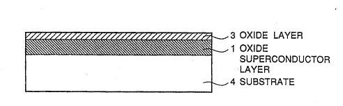
Figure 1 shows a diagrammatic sectional view of one preferred
embodiment of the superconducting thin film in accordance with the
present invention. In Figure 1, a superconducting thin :film includes an
oxide superconductor layer 1 formed of a YlBa2Cu307 ~ oxide
superconductor material on a MgO (100) substrate ~ and an oxide layer 3
stacked on the oxide superconductor layer 1.
l'he oxide superconductor layer 1 is composed of a c-axis orientated
YlBa2Cu307.~ crystalline oxide superconductor layer in which crystalline
lattices are disposed to constitute one unit-cell layer. The oxide
superconductor layer 1 has a thickness of about 1~2 nanometers.
The oxide layer 3 is constituted of a crystalline BaCuO2 layer, of
which one unit-cell is the same as a half unit-cell of the YlBa2Cu307 ~
oxide superconductor crystalline lattice~ or a crystalline PrlBa~Cu307.
layer which has a similar crystal st3ucture to that o~ the YlBa2(:u307.~
oxide superconductor~ 'rhe oxide layer 3 should be eomposed of a
complete crystalline layer of the above oxides in which c~stalline lattices
are disposed at least one unit-cell thick.
- 7 -
. .. ~.
In case o:f BaCuO2, the oxide layer 3 has a thickness of about 0.5
nanometers, and in case of PrlBa2Cu3O7~e~ the oxide layer 3 has a
thlCkIleSS of about 1.2 nanomcters.
The oxide layer 3 compensates for a bared Cu O plan~ at tl~e outer
most surface of the YlBa2Cu3O7.~ oxide superconductor la~rer 1 so th~t
superconducting current flows ~hrough the oxide superconduc~or layer 1
in which YlBa2Cu3O7.g crystalline lattices are disposed to constitute one
unit-cell layer. Therefore, the a~ove superconducting thin film in
accordance with the present invention show superconductivity, though ~e
oxide superconductor lay~r 1 is composed of ~le YlBa2Cu307.~ crystalline
layer which has a thickness of only one unit-cell.
The above superconducting thin film in accordance with the present
invention was prepared by ~he ~ollowing process.
At first, a crystalline YIBa2Cu307.~ ox;de superconductor layer 1
was deposited on a principal sur~ace of a MgO (100) single crystalline
substrate 4 by MBE. ~7hile the YlBa2Cu307 ~ oxide superconductor layer
1 was growing, the surface morphology of the Yl13a2Cu307 ~ oxide
supe~conductor layer 1 was monitored by RHEED so that the atomic
layers which constituted ~he YlBa2Cu307 ~ crystals were accurately
stacked layer by layer so as to compose one unit-cell layer of ~e
YlBa2Cu307 ~ clystalline latices.
A condition of forming ~e c-axis orientated YlBa2Cu307~ oxide
superconductor layer 1 by MBE was as follows:
Molecular beam source Y 1250C
Ba: 600C
Cu: ~040~
Pressure 1 x 10⁻⁵ Torr
-. ..
~r~8~
Temperature of ~e substrate 700DC
Thickness 1.2 nanometers
Then, the Y molecular beam source was shuttered so that an oxide
layer 3 composed of BaCuO2 oxide thin film was continuously fo~med on
the YlBa2Cu30~.~ oxide superconductor layer 1. The BaCuO2 oxide thin
film was composed of a BaCuO2 crystalline layer in which crystalline
lattices were disposed to constitute one unit-cell layer.
A condition of forming the BaCuO2 oxide thin film by MBE was as
follows:
Molecular beam source Ba: 600C
C~: 1040C
Pressure 1 x 10⁻⁵ Torr
Temperature of the substrate 700C
Thickness 0.5 nanometers
Then the superconducting thin film in accordance with the present
invention was completed. The superconducting thin ~ilm prepared by ~e
above process showed superconductivity, though the superconducting
layer was composed of YIBa2Cu3O7 ~ crystalline lattices which were
disposed to constitute one unit-cell layer. Electrical resistance of the
superconducting thin film disappeared a~ the temperature of 87K so ~at
the superconductin~ thin fi~n showed superconductivity.
Another superconduc~ing thin film of which the oxide layer was
constituted of PrlBa2Cu3O7 ~ oxide ins~ead of BaCuO2 was prepared by a
similar process as mentioned above.
This superconducting thin film was manufactured by almost same
method as the above mentioned method. There~re~ the difference will be
described in the ~ollowing.
g
~7~
When the superconducting thin film which utilized Prll3a2Cu307
for ~e oxide layer 3 was manu~actured, in order to form the ~xide l~yer
3, the Y molecular beam source was switched to ~he Pr molccular beam
source so that an oxide layer 3 composed of PrlBa2(:u307 oxide thin
lm was continuously fo~ned on the YlBa2Cu~O7 ~ oxide superconductor
layer 1 when the YIBa2Cu307.~ oxide superconductor layer 1 was
completed. The PrlBa2Cu307.~ oxide thin :film was composed of a
PrlBa2Cu307 s, crystalline layer in which crystalline lattices were disposed
to constitute one lmit-cell layer.
A condition of forming ~e PrlBa2Cu307 ~ oxide thin ~llrn by MBE
is as follows:
Molecular beam source Pr: 1225C
Ba: ~00C
Cu: 1040~C
Pressure 1 x 10⁻⁵ Torr
Temperatur~ of the substrate 700C
~hiclcness 1.2 nanometers
Tben, the superconducting thin film in accordance with the present
invention which included one unit-cell YlBa2C~3~7 ~ oxide
superconductor crystalline layer and one unit~cell PrlBa2Cu307~ oxide
crystalline layer was completed. The superconducting ~in film prepared
by the above process showed superconductivity, though the
superconducting layer was ~omposed of YlBa2Cu307 ~ crystalline lattices
which were dispvsed-to constitute one unit-cell layer. Electrical resistance
of ~e su~erconducting thin film disappeared at the temperatllre of 85K so
~at ~e superconducting ~in ~llm showed superconductivity.
2~7~
Embodime1lt 2
Figure ~ shows another preferred embodiment of the
superconducting thin film in accordance with the present invention, in
which the superconducting thin film has multiple oxide ~uperconductor
layers 11 and 12 and oxide layers 31, 32 and 33 on a substrate 4.
The oxide superconductor layers 11 and 12 are composed of c-axis
orientated YIBa2Cu307 ~ cryst~lline oxide superconductor layers in which
crystalline lattices are disposed to constitute one unit-cell layers. Fach of
the oxide superconductor layer 11 and 12 has a ~hickness of about 1.2
nanometers.
The oxide laye~s 31, 32 and 33 are constituted of a crystalline
PrlBa2Cu307.~ layers. Each of the oxide layer 31, 32 and 33 should be
cornposed of a complete crystalline layer of the above oxides in which
crystall;ne lattices are disposed at least one uni~-sell thick~
In this embodiment, the oxide layer 31 is compcsed of the
crystalline PrlBa2Cu307.~ oxide layer in which three unit-cells of ~e
crystalline lattices are stacked. The oxide layers 32 and 33 are composed
of the crystalline PrlBa~Cu307 ~ oxide layers in which two unit-cells of
crystalline lattices are stacked. The oxide layer 31 has a ~ickness of
about 3~5 nanometerg, each of the oxide layers 32 and 33 has a thickness
of about 2.5 nanometers.
Th~ current capability of the one unit-cell crystalline ~IBa2Cu307 ~
oxide superconductor layer is de~lned by the critical current density Jc f
YlBa2Cu307 ~ oxide superconduc~or~ ~herefore, the current ~apability of
the superconducting thin film is determined lby number of ~he
YlBa2Cu307 ~ oxide superconduc~or unit-cell layers. Namely, it is
possible to control subs~an~ial ~arrier density of the superconducting ~hin
2 ~
~ilm accurately by changing the number of the YlBa2Cu307 ~ oxide
superconductor layers per unit thickness.
In ~is connection~ the c~stal unit cell thickness of YIBa2Cu3()
oxide superconductor are almost the same as that of PrlBa2Cu30~ e oxide.
~here~ore, it is possible to manufacture the superconducting thin film
which ha~ various current capability but the same thickness by changing
~he number ~f the PrlBa2Cu307.~ oxide unit-cell layers contained in the
superconducting thin film.
The above superconducting ~in film in accordance wi~ the present
invention was prepared by repeating the process of Embodiment 1.
Namely, at first a Prl:13a2Cu307 oxide layer 31 having a thickness OI
about 3.5 nanometers was deposited on a principal sur~ace of a MgO
(100) substrate 4 by an MBE method~ In this comlection, the atomic
layers which constituted the PrlBa2Cu307 E crystals were accur~tely
stacked layer by layer or unit by UIlit so that the PrlBa2Cu307 ~ oxide
layer 31 was composed of a PrlBa2Cu307 ~ crystal layer in which three
unit-cells of the crystalline lattices were stacked. An MBE condition
under which the PrlBa2Cu307 ~ oxide layer 31 was ~ormed was ~e same
as the first embodiment~
Then~ the Pr molecular beam source was switched to the Y
molecular beam source so that a YlBa2Cu307 ~ oxide superconductor
layer 11 having a thickness of about 1.~ nanometers was continuously
fo~ned on the PrIBa2Cu307 ~ oxide layer 31. The YlBa2Cu307 ~ oxide
superconductor layer 11 was composed of a YlBa2Cu30~ ~ crystalline
layer in which crystalline lattices are disposed to constitute one unit-cell
layer. An MBE condition under which the YlBa2Cu307 ~ oxide
superconductor layer I 1 was formed was same as the first embodiment.
- 12-
.. ~-
Thereafter, the Y molecular beam source was switched to the Pr
molecular beam source again so that a PrlBa2Cu307 ~ oxide layer 32
having a thickness of about 2.5 nanometers was continuously ~ormed o~
~e Y~Ba~Cu307 ~ oxide superconductor layer 11. ~e PrlBa2Cu307 e
oxide layer 32 was composed of a PrlBa2Cu307 ~ crystal layer in whi~
two unit-cells of the crystalline lattices were stacked. An M:~E condition
und~r which the PrlBa2Cw307 E oxide layer 32 was formed was same as
~e process under which the PrlBa2Cu307 E oxide layer 31 was forrned.
After then, the Pr molecular beam source was switched to the Y
molecular beam source so that a YIBa2Cu307 ~ oxide superconductor
layer 12 having a thickness of about 1.2 nanometers was con~inuously
formed on ~e PrlBa2(:u307 E oxide layer 32. The YIBa2Cu30~ ~ oxide
superconductor layer 12 was also comp~sed of a YIBa2Cu307 ~ crystalline
layer in which crystalline lattices are disposed to constitute one unit-cell
layer. An MBE condition under which the Y~Ba2Cu307 ~ oxide
superconductor layei 12 was ~o~ned was same as the process Imder which
~e YIBa2~u307 ~ oxide superconductor layer 11 was formed.
Thereafter, the Y molecular beam source was switehed to the Pr
molecular beam source again so that a PrlBa2Cu307 o~ide layer 33
having a thickness of about 2.5 nanometers was continuously fonned on
the YIBa2Cu307 ~ oxide superconductor layer 12. I'he PrlBa2Cu307 ~
oxide layer 33 was also composed of a Pr~Ba2Cu307 ~ crystal layer in
which two unit-cells of the crystalline lattices were stacked. An MBE
condition under which the PrlBa2CIl307 E oxide layer 33 was ~o~ned was
same as the process under which the PrlBa~Cu3C)7 E oxidc layer 31 was
formed.
- 13-
.. . . . ~ , ,
.
2 ~ p~
Then, the superconducting thin film in accordance with the present
invention which included two one-unit-cell YlBa2Cu307 ~ o~ide
superconductor crystalline layers and three PrlBa2cu3o7~e oxide
c~stalline layers was completed. The superconducting thin ~ilm prepa~ed
by the above process showed superconductivity, though each of the
superconducting layers was composed of ~IBa~Cu307~ crystalline lattices
which were disposed to collstitute one unit cell layer. E~lectrical resistance
of each of the superconducting layers disappeared at the temperature of
85K so that the superconducting ~hin ~llm showed superconductlvity.
Embodiment 3
Figure 3 shows a supercorlducting device (super-FET) in
accordance with ~he present invention which has a superconduc~ing
channel 10 utilizing a superconducting thin i~ilm similar to ~he
superconducting thin film of Embodimen~ 2 which has two one-unit-cell
YlBa2Cu307 ~ oxide superconductor crystalline layers and three
one-unit-cell PrlBa2Cu307~ oxide crystalline layers.
The super-FET has a substrate 4 on which the superconducting
channel 10 is arranged. The substrate 4 can be fo~med of an insulating
substrate, preferably an oxide single crystalline sulbs~rate such as MgO,
~rTiO3, CdNdAl04~ etc. These substrate materials are very effective in
forming or growing a crystalline film having a high degree of
crystallinity.
A superconducting source electrode 5 and a superconducting drain
electrode 6 which are composed of an oxide supcrconductor are arranged
at ~e both sides of the superconducting channPI 10 on the substrate 4.
The superconducting source electrode S and the superconduGting drain
- 14-
20 ,$~
electrode 6 are electrically connected through the supercondwcting
channel 10 so that superconducting current flows between the
superconducting source electrode S and the superconductillg drain
electrode 6.
The superconducting source electrode S and the superconducting
drain electrode 6 are preferably composed of the same oxide
superconductor which is used for ~2e superconducting channel 10. In ~is
embodiment, ~ey are composed of a-axis orientated YlBa2Cu307 ~ oxide
superconductor thin films.
A gate elec~rode 7 is staeked on a gate insulator 8 which is arranged
on the superconducting channel ln. The superconducting cu~r~nt flowing
through the supercondueting channel 10 is eontrolled by a vol~age which
is applied to the gate electrodeO The gate electrode 7 is composed of Au
and ~e gate insulator 8 is composed of SrTiO3.-
In order to obtain a complete ON/O~F operation, both of thesuperconducting channel and the gate insulator of this type of super-PET
should h~ve an extremely thin thickness. Por example, the
superconduGting charmel formed of an oxide supercondllctor material
should have a thickness of less ~an five nanomelers, and ~he gate insulator
should have a thickness more ~han ten nanomcters which is su~ficient to
prevent a tunnel ~urrent.
The superconducting channel 10 of the above super-FET is
composed of a superconducting thin film such as Embodiment 2.
Therefore, it is possible to control the carrier density of the
supereonducting ehannel 10 by changing the number of the oxide
superconductor layers and ~he oxide layers while thickness of ~he
supercoIlducting channel 10 is kept constant.
- 15-
- ,. . ~-.. .... ~ ,. .
. ~ . . ., ~
. . . ~, - . , . -
:- ,
, -i ~, .. . . .
. - ~
2 ~ r~
By thiæ, the super-FET in accordance wi~ ~e present invention can
have var~ous current capabilities.
Embodiment 4
Figure 4 shows a tunnel type Josephson device in accordance with
the present invention. The Josephson device has a substrate 4, a ~irst
oxide superconductor layer 1 formed on the substrate 4? an oxide layer 3
formed on the first oxide superconductor Iayer 1 and a second oxide
superconductor layer formed on the oxide layer 3.
~ he first and second oxide superconductor layers 1 and 2 are
formed of crystalline YlBa2Cu3O7.~ oxide superconductor having a
~ic~ess of 200 nanometers and the oxide Iayer 3 is fonned of clystalline
PrlBa2Cu307 ox;de having a thickness of 5 nanome~ers.
The above Josephson device in accordance with the present
inven~ion was manufactured by ~e following process.
At first, a crystalline YIBa2Cu307.~ oxide superconductor layer 1
having a thickness of 200 nanometers was deposited on a principal surface
of a MgO (100) single crystalline su~str~te 4 by an M~3E. An MBE
condition under which the YIBa2Cu307 ~ oxide superconductor layer 1
was fo~med was the same as the first embodiment.
~ hen, the Y molecular beam source was switched to the Pr
molecular beam source so tha~ a PrlBa2Cu307 oxide layer 3 having a
thickness of about 5 nanometers was continuously formed on the
YIBazCu3O7.~ oxide superconductor layer 1. ~he PrlBa2Cu3O7 ~ oxide
layer 3 was composed of a PrlBa2Cu3O7.e crystaI layer in which ~our
uni~-cells of the crystalline Iattices were stacked. An MB~ condition
- 16-
... .... - .. :
:~
~7~
under which the Pr~Ba2Cu307. oxide layer 3 was formed was same as ~e
the ~Irs embodiment.
Thereafter, the Pr molecular beam source was switched to the Y
molecular beam source so that a crygtalline YlBa2Cu307~ oxide
superconductor layer 2 having a thickness of about 200 nanometers was
continuously ~ormed on the Pr1Ba2Cu307 p oxide layer 3. An MBE
condition under which the YlE~a2(:~u307 ~ oxide superconductor layer 2
was formed was same as the process under which the YIBa2Cu307.g oxide
superconductor layer 1 was foImed. Metal electrodes were formed on the
oxide superconductor layer 1 and 2, if necessary.
With this, the Josephson device in accordance with the present
invention was completed.
A current-volta~ge characteristics of the above mentioned Josephson
device was me~sured at a temperature of 85K. When a microwave of 15
G~z was irradiated, clear Shapiro steps were observed, therefore, it could
be ascertained ~at the Josephson junction was reali~ed in the device.
On the contrary, in a conventional Josephson device ~f which the
oxide layer 3 was formed of MgO, as shown in Figure 5, upper portion
11 of the YIBa2Cu307 ~ oxide superconductor layer 1 and bottom portion
21 of the YlBa2Cu307 ~ oxide superconductor layer 2 did not show
superconductivity so that little Shapiro steps were observed.
The invention has thus been shown and described with reference to
the specific embodiments. However, it should be noted tha~ the present
invention is in no way limited to the de~ails of the illustra~ed structures
but converts a~d modifications may be made within the scope of the
appended claims.
- 17 -
: . : . ~.. ; : :
.. , . . : . : ~: