Note: Descriptions are shown in the official language in which they were submitted.
wo 91/15053 PCT/DE91/00135
1- 2~7~
~lectronic Switching Power Supply
This invention relates to an electronic switching
power supply for supplying power to a load from an input
voltage source, including a flyback converter with a
transformer having its primary coil connected in series
with the collector-emitter circuit of a first transistor
in parallel arrangement with the input voltage source,
while its secondary coil is connected in series with the
load and a first diode, with the emitter of the first
transistor being connected to chassis or reference poten-
tial through a first resistor while the base of the first
transistor is connected to a control circuit, with a
capacitor in parallel arrangement with the load, with the
voltage across the junction of the capacitor at the side
remote from reference potential being of the same
polarity as the voltage across the junction of the first
resistor and the first transistor.
Electronic switching power supplies are used for de-
livering a constant voltage and/or a constant current to
electrical or electronic devices, being frequently con-
structed as primary or secondary switched-mode f}yback or
~orward converters or as push-pull converters. As a
rule, they include a rectifier circuit with a subse~uent
filtering and smoothing arrangement to which a trans-
former is connected. An electronic switch is provided
which is connected in series with the primary coil of the
transformer and is turned ON and OFF in dependence upon
one or several control variables, with the energy stored
in the transformer being delivered to an elestrical load
through a diode of suitable polarity during the reverse
period where a flyback converter is used, during the for-
ward period where a forward converter is used, and during
both the reverse and the forward period where a push-pull
converter is used.
A switching power supply of the type initially re-
ferred to is known, for example, from EP 0 130 411 Bl.
The embodiment shown in FIG. 2 of this specification in-
corporates a self-oscillating flyback converter, that is,
the control circuit connected to the base of the ~irst
transistor is substantially comprised of the ~eedback
from the secondary circuit through a capacitor and a re-
sistor to the base of the first transistor, as well as a
second transistor having its collector-emitter circuit
between the base of the first transistor and reference
potential, its base receiving the voltage drop across the
first resistor. However, the present invention being not
- . . ,, ...................... .... . ............. ~ .
.. . .
-: , ~. . : , : -
Wo 91/15053 PCT/D~91/00135
' 2 ~ 2~78~ ~3
limited to a switching power supply with a self-
oscillating flyback converter, it also finds application
in switching power supplies having a master-excited
flyback converter. In such an arrangement, the control
circuit comprises, for example, a multivibrator whose
clock frequency or pulse/no-pulse ratio driving the base
of the first transistor varies in dependence upon the in-
put voltage, the primary current, and/or the secondary
current.
Depending on the application, such switching power
supplies are conventionally designed for supplying a pre-
determined (m~ r) operating current. In some applica-
tions, however, the load which may be, for example, the
~otor of a small electrical appliance such as a shaver or
a hair-removing appliance, requires a starting current
substantially higher than its operating current. Under
such conditions, it would be only because of the
temporary need for a higher starting current that the
switching power supply would have to be designed for peak
currents substantially higher than required by the load
in operation, accordingly resulting in an increased power
dissipation also on termination of the startup phase
because of the higher primary peak current. For example,
the first resistor arranged in the primary circuit would
have to be su~stantially smaller to enable a higher
primary peak current to flow, which would above all
produce higher losses in the switching transistor.
It is therefore an object of the present invention
to configure an electronic switching power supply of the
type initially referred to in such a ~anner as to enable
it to deliver a higher starting current to the load with-
out involving the need for a higher primary peak current
during operation, that is, on termination of the startup
phase.
~ .~
This object is accomplished by the present invention
in that a second resistor is placed between the junction
of the first resistor ~nd the first transistor and the
junction o~ the capacitor at the side remote from ref-
erence potential.
Because the current delivered by the flyback con-
verter is proportional to the emitter resistance of the
switching transistor, the solution of the invention pro-
vides a simple means of supplying through the second
resistor an additional primary current in the startup
phase, that is, during the period of time when the
voltage across the load is of a magnitude smaller than
the ~ voltage drop across the first resistor, the
-........ . . , . :, . .: . ,
,: . . ,.,. . . , . :
~: :.; .. - :. . . . . . . . , . - : . ,
". , . :.
. :: : : : .- , . : -
,
:.~, : . :.- - - , -
.: :' - , -. :
WO 91/15053 PCr/D139~ /00135
- 3 - 2.~,7~73
second resistor being then connected in parallel with the
first resistor through the load.
In an advantageous embodiment of the present inven-
tion, a second diode is connected in series with the
second resistor.
Connecting a diode in series has the advantage that
the second resistor is turned off automatically when the
voltage across the load has attained the magnitude of the
maximllm voltage drop across the second resistor.
Further advantageous e~bodiments will become
apparent from the other subclaims.
The invention will be described in greater detail in
the following with reference to embodiments illustrated
in the accompanying drawings.
In the drawings,
FIG. 1 is an electrical schematic illustrating an
embodiment of the invention;
FIG. 2 is a circuit configuration of a switching
power supply with a self-oscillating flyback converter;
and
FIG. 3 is a graph showing the pri~ary peak current
Ia plotted against the load voltage Uo using a second re-
sistor (broken line), and using a second resistor and a
second diode in series arrangement (solid line).
The schematic of an electronic switching power
supply shown in FIG. 1 is comprised of a flyback con-
verter energized from a dc or ac supply 20 through a
bridge rectifier arrangement 3. An input capacitor 4 for
filtering and smoothinq the input voltage is connected in
parallel with the dc voltage input terminals of the
bridg~ rectifier arrangement 3.
Connected in parallel with the input capacitor 4 is
the series arrangement comprised of the primary coil 51
of a transformer 5 and the load circuit of a first
transistor 1 and a first resistor 8.
The cecond~ry coil 52 of the transformqr 5 is
series-connected to a diode 7 and a parallel circuit com-
prised of a capacitor 16 and a load 6.
The base of transistor 1 is driven by a control
circuit St. ~he configuration of the control circuit St
, . , .: ,. : ~. .: ......................... : ; .
, " , ,, , . . - - : : : .
Wo 91/15053 PCT/DE91/00135
- 4 - 2~7~5~3
may vary, depending also on whether the flyback converter
is of the self-oscillating or master-excited type.
Between the junction A co~necting the emitter of the
switching transistor 1 to the resistor 8 and the junction
B connecting the capacitor 16 to the load 6 at the side
remote from reference potential, a series circuit com-
prised of a resistor 81 and a diode 82 is arranged.
Diode 82 may also be a Zener diode. In this embodiment,
the diode has its cathode connected to junction B,
because transistor 1 is an NPN transistor. If a PNP type
transistor is used, diode 82 must have its cathode
connected to junction A.
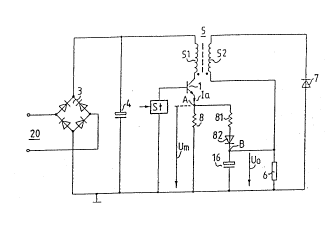
FIG. 2 shows the detailed circuit arrangement of a
switching power supply with a self-oscillating flyback
converter.
The base of transistor 1 is connected to the one end
of the primary coiI 51 of the transformer 5 through a re-
sistor 12, to the one end of the secondary coil 52 of the
transformer 5 through the series arrangement comprised of
a feedback capacitor 9 and a feedback resistor 10, and to
the collector of a transistor 2 having its emitter con-
nected to the one dc teL ina~ of the bridge rectifier
arrangement 3 through a switch 17.
Through a first reference element in the form of a
Zener diode 11, the base of transistor 2 is connected to
the other end of the secon~Ary coil 52 of the transformer
5 and to the ou~puL capacitor 16 or the dc motor 6, and,
through a second reference element in the form of a Zener
diode 22, to the emitter of the first transistor 1~ In
parallel arrangement with the base-emitter circuit of
transistor 2 is a resistor 13, a capacitor 14 being pro-
vided parallel to resistor 8.
The series arrangement comprised of a Zener diode 18
and a diode 19 of a polarity allowing current to flow in
opposite direction, their respective cathodes being
interconnected, serves the function of eliminating or
limiting the peaks of the voltage kick-back pulses re-
sulting from leakage inductance.
In parallel arrangement with the feedback capacitor
9 is a diode 15 having its anode connected to the one end
of the secondary coil 52 of the transformer 5.
. .: .:. .. : . :
. . .
wo 91/15053 PCT/DB91~00135
- 5 - 2~ 3
Accordingly, in FIG. 2 the control circuit St (FXG.
1) is substantially comprised of the feedback capacitor
9, the feedback resistor 10, and the transistor 2. In
lieu of transistor 2, a Zener diode may be arranged ~e-
tween the base of transistor 1 and reference potential.
This Zener diode will be conducting when the voltage (Um)
dropping across the resistor 8 plus the base-emitter
voltage of transistor 1 have attained the magnitude of
the Zener voltage of the Zener diode. In this event, th~
control circuit must be connected to the emitter of tran-
sistor 1.
The series circuit comprised of resistor 81 and
diode 82 is placed between the emitter of the switching
transistor (junction A) and the cide of the dc motor 6
remote from reference potential (junction B).
It will be understood that an accumulator used for
operation of the dc motor 6 independently of the line may
be provided parallel to the dc motor 6 through a corre-
sponding switch arrange~ent.
In the following, the ~ode of operation of the
switching power supply of FIG. 2 will be described as if
the resistor 81 and the diode 82 were omitted.
When an ac line voltage i8 applied to the bridge
rectirier arrange~ent 3, the rectified ac voltage is
supplied to the smoothing and filteri~g capacltor 4, so
that the ~-iu~e~ flowing through the primary coil 51 of
the tran6former 5 and the resi6tor 12 charges the feed-
back capacitor 9 through the feedback resistor 10 until
the voltagè on the base of kransistor 1 has increased to
a value rendering transistor 1 conducting. ~he collector
current thereby produced flow~ through the primary coil
51 of the transformer 5, inducing in the secondary coil
52 a positive voltage which i6 delivered through the
feedback capacitor 9 and the feedback resistor 10 to the
base of transistor 1, producing a higher base ~urLen~.
With transi6tor 1 turned on, the ~iuL~e~ flowing through
the primary coil 51 of the transformQr 5 will rise
linearly a~ a result of the inductance of the primary
coil 51, until a voltage which is proportional to the
linearly rising current drops across resistor 8, which
voltage, from a predetermined magni~ude on, allows a base
current to flow in transistor 2, turning on the second
transistor 2 a~d pulling the potential on the base of
transistor 1 down to reference potential, turning tran-
sistor 1 off. During the off period of transistor 1, the
-~I.eLic energy stored in the core of the transformer 5
is delivered through the se~on~Ary coil 52 and the diode
7 to the output capacitor 16.
..
.,
~, - - . ,
. .
, .:
WO 91/15053 PCr/DE91/00135
.,
- 6 - 2 ~ 7 ~ 3 ~
When the voltage residing at the output capacitor 16
exceeds the Zener voltage of the Zener diode ll as a re-
sult of the charging condition of the output capacitor
16, transistor 2 will be maintained conducting, indepen-
dently of the voltage drop across resistor 8, so that
chassis or reference potential is always maintained at
the base of transistor 1, as a result of which the
flyback converter stops operating. Only when, as a
result of the current consumed by the parallel-connected
dc motor 6, the voltage across the output capacitor 16
has dropped to a value below the Zener voltage of the
Zener diode 11, will the off or on state of transistor 2
and thus of transistor l become dependent again on the
voltage drop across resistor 8 with respect to the Zener
voltage of the zener diode 22, and the flyback converter
is able to start oscillating again.
The Zener diode 22 serves the function of placing
transistor 2 in conduction when the Zener voltage of the
Zener diode 22 is exceeded as a result of the voltage in-
crease across the emitter resistor 8.
. : .
The parallel arrangement of the diode 15 and the
feedback capacitor 9 enables the flyback converter to
resume oscillation promptly when the voltage falls below
the Zener voltage of the Zener diode 11, because the out-
put voltage residing at the secondary coil 52 of the
transformer 5 immediately provides through the diode 15 a
polarity driving transistor 1.
Assuming, for example, a pri~ary peak current Ia of
O.5 A and an emitter resistance of 10 ohms (excluding
resistor 81 and diode 82), the -~i peak voltage
dropping across the emitter resistor is Um = 5 V. The
peak current occurring in the secondary circuit is pro-
portional to the primary peak current. If the thus
attainable arithmetic mean of the current passing through
the load 6 is not sufficient, the primary peak current
must be increased. This could be accomplished, for
example, by making the emitter resistor 8 smaller.
However, if the load 6 which, for example, is a dc motor,
requires an increased current only in the startup phase,
this solution would produce ~lnnec~s~ily high switching
losses in transisto~ 1 also in the normal operating mode,
because the primary peak current r~ ~i n~ unchanged.
To supply the load 6 with a higher starting current
producing a correspondingly higher motor starting torque,
resistor 81 and diode 82 are inserted between junction A
and junction B. The mode of operation of this configura-
tion will be explained with reference to FIG. 3. In this
Figure, the pri~ary peak current Ia is plotted against
'~ ~: ' . :
.. '~ ~ '
,1." ' ' ~ ' . ,
, .
Wo 91/150S3 PCT/D~gl/00135
- 7 - 2~7~7~
the voltage Uo residing at the load 6 and at the capaci-
tor 16 when power is turned on. The voltaqe Uo is thus a
function of time. Resistor 81 and resistor 8 have each a
resistance of 10 ohms, the operating voltage of the load
is Uo = 10 V. At the instant that power is turned on and
neglecting the forward voltage of diode 82, the primary
peak current is Ia = 1 A instead of the previous 0.5 A,
because at this instant the voltage across junction B is
o V with respect to reference potential.
The following equation applies:
Ia = ~m + Um - Uf - Uo
R8 R81
where Uf is the forward voltage of diode 82. With
the output voltaqe Uo rising (rotational frequency of
motor increasing), the amplitude of the primary peak
current Ia will decrease.
If both the resistor 81 and the diode 82 are
arranged between junctions A and B, the solid line drawn
in FIG. 3 shows the characteristic of Ia as a function of
Uo (neglecting Uf). When Uo = S V which corresponds to
the maximum voltage Um across resistor 8, the primary
peak current will have dropped to 0.5 A. If the voltage
Uo subsequently increases to a magnitude exceeding 5 V,
resistor 81 will ~e turned o~f automatically, since diode
82 is cut off. The primary peak current la is 0.5 A, as
before without the resistor 81.
Diode 82 may also be omitted. With such a configu-
ration, the broken line drawn in FIG. 3 resultsO If the
voltage Uo then exceeds the voltage U~ (at 5 V~, that is,
the potential across junction B is greater than across
junction A, the primary peak current Ia will continue to
drop, yet an additional current will flQw from the
secondary circuit through resistor 81 and resistor 8 to
reference potential. While the purpose to achieve a
higher starting current is equally well accomplished in
the absence of diode 82, the power dissipation under
operating conditions is greater than it would be in the
presence of diode 82 because of the ~ eot flow from B
to A through resistor 81.
Without diode 82, the following equation applies:
Uo = R8 + R81 ~ Um
R8
. . .. . . . .