Note: Descriptions are shown in the official language in which they were submitted.
207873~
BROADBAND MICROSTRIP TO SLOTLINE TRANSITION
BACKGROUND OF THE INVENTION
The present invention relates to improvements in the
transitioning between microstrip and slotline microwave
transmission lines.
Flared slot radiators are becoming increasingly
popular in active radar arrays because of their broadband
characteristics and suitability to active array architec-
tures. Presently, a new frequency dependent microstrip to
slotline transition must be designed for each application.
Conventional transitions between microstrip and
slotline transmission lines have utilized either an inter-
mediate transmission line type, such as parallel strip, or
frequency dependent tuning stubs. These conventional
transitions therefore require more area on the circuit
broad, and also are limited in frequency bandwidth.
It is therefore an object of an aspect of the invention
to provide a broadband transition between microstrip and
slotline transmission lines.
SUMMARY OF THE INVENTION
The invention is a transition between two types of
transmission lines, microstrip lines and slotlines. What
is new about this particular transition is the geometry
employed in integrating the two transmission line types at
.~.
--
2 207873h
the transition. The geometry used results in a broadband
microstrip short circuit across the slotline and a broad-
band slotline open circuit in the direction opposite of
propagation on the slotline. These two characteristics are
required for direct coupling from the microstrip to the
slotline. There are no intermediate transmission line
types between the microstrip and the slotline, and no
frequency dependent tuning stubs are used to produce the
short circuits and open circuits required for coupling.
The result is a broadband transition which can be fabricat-
ed using standard etching techniques and requiring no
plated through holes.
Other aspects of this invention are as follows:
A broadband microstrip to slotline transition,
comprising:
a dielectric substrate having first and second
opposing surfaces which are coated with respective
patterned electrically conductive regions defining the
ground planes and transmission lines of said micro-
strip and said slotline transmission lines;
said microstrip transmission line comprising a
microstrip conductor line defined by said patterned
regions on a first one of said opposing surfaces and
a ground plane defined by said patterned regions on
the second one of said opposing surfaces;
said slotline transmission line comprising first
and second groundplanes defined by respective ones of
said patterned regions on said respective first and
second surfaces;
said second groundplane of said slotline trans-
mission line also serving as said groundplane of said
microstrip transmission line; and
-
2078736
2a
wherein said microstrip transmission line transi-
tions into said first groundplane of said slotline
transmission line in a transition region defined on
said first region, thereby creating a broadband
microstrip shunt across said slotline at the point of
intersection of said microstrip and slotline transmis-
sion lines and also creating a broadband slotline open
circuit at one end of the slotline transmission line,
thereby creating strong coupling between the micro-
strip and the slotline.
A double-sided flared slot radiator having a
microstrip feed circuit, comprising:
a dielectric substrate having first and second
opposed surfaces;
a first flared radiator region defined on said
first surface by a first conductive region on said
first surface;
a second flared radiator region defined on said
second surface by a second conductive region on said
second surface;
said first and second flared radiator regions
defining a radiator notch at an area of overlap of
said radiator regions;
a microstrip transmission line comprising a
conductor line defined on said first dielectric
surface by a transmission line conductive region, and
a groundplane defined by said second flared radiator
region, said transmission line transitioning directly
into said first flared region adjacent said notch;
wherein said first and second radiator regions
define a double sided slotline transmission line in
the vicinity of said notch; and
. ~ "` . _
207873~
2b
wherein a broadband microstrip shunt circuit
occurs across said slotline transmission line and a
broadband slotline open circuit occurs at one end of
said slotline transmission line, thereby resulting
in strong coupling between microstrip and said
slotline.
A double-sided flared slot radiator having a
microstrip feed circuit, comprising:
a dielectric substrate having first and second
opposed surfaces;
a first flared radiator region defined on said first
surfaces by a first conductive region defined on said
first surface;
a second flared radiator region defined on said
second surface by a second conductive region on said
second surface;
said first and second flared radiator regions
defining a radiator notch at an area of overlap of said
radiator regions;
a microstrip transmission line comprising a
conductor line defined on said first dielectric surface
by a transmission line conductive region, and a ground-
plane defined by said second flared radiator region, said
transmission line transitioning directly into said first
flared region adjacent said notch;
wherein said first and second radiator regions
define a double sided slotline transmission line in the
vicinity of said notch;
said slotline transmission line having a
longitudinal axis along said dielectric substrate and
said conductor line being transverse to said longitudinal
axis in the vicinity of said notch; and
2n78736
wherein a broadband microstrip shunt circuit occurs
across said slotline transmission line and a broadband
slotline open circuit occurs at one end of said slotline
transmission line, thereby resulting in strong coupling
between said microstrip and said slotline such that wave
propagation and corresponding energy down the slotline is
in one direction toward output end and energy incident on
the transition from the slotline is in strong coupling
into the microstrip transmission line, so that energy is
launched from the microstrip into the slotline and into
free space.
BRIEF DESCRIPTION OF THE DRAWING
These and other features and advantages of the present
invention will become more apparent from the following
detailed description of an exemplary embodiment thereof, as
illustrated in the accompanying drawings, in which:
FIG. 1 is a top view of a microstrip to slotline
transition in accordance with the invention.
FIG. 2 is an output end view of the transition of FIG.
1.
FIG. 3 is an input end view of the transition of FIG.
1.
FIG. 4 is a bottom view of the transition of FIG. 1.
FIG. 5 is a top view of a doublesided printed flared
slot radiator embodying the invention.
FIG. 6 is a bottom view of the flared slot radiator of
FIG. 5.
FIG. 7 is an overlay view showing the radiator ele-
ments formed on the top and bottom side of the transition
of FIG. 5.
L~
207873~
FIG. 8 is a graph illustrating the measured VSWR of an
exemplary transition embodying the invention as a function
of frequency.
DETAILED DESCRIPTION OF THE PREFERRED EMBODIMENT
A microstrip to slotline transition in accordance with
the invention is formed by integrating a microstrip trans-
mission line with a double sided slotline, as shown in
FIGS. 1-4. As is well known, a microstrip transmission
line is a two wire transmission line formed by a conducting
strip located over a conducting groundplane. The charac-
teristic impedance of the microstrip line is determined by
the width of the conducting strip, its height above the
groundplane, and the dielectric constant of the material
between the two. A double-sided slotline is a slot trans-
mission line formed by the co-linear adjacent edges of two
conducting groundplanes which are located on opposite sides
of a dielectric slab. The characteristic impedance of the
double-sided slotline is determined by the amount of
overlap of the two edges of the groundplanes which form the
slotline, the thickness of the dielectric slab between
them, and the dielectric constant of the slab material.
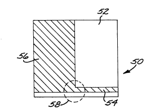
FIG. 1 is a top view of the transition 50, and shows
the conductive regions as cross-hatched areas on the top
surface of the dielectric substrate 52; the conductive
regions define various elements of the transmission lines.
The conductive layer on the top surface defines a micro-
strip transition line 54, one of the slotline groundplanes
56, and a transition region 58. The microstrip transition
line 54 joins the groundplane 56 at the transition 58.
FIG. 2 is an output end view of the transition 50 of
FIG. 1 showing the slotline groundplanes 56 and 60 for a
double-sided slotline.
207~736
FIG. 3 is a transition end view showing the microstrip
conductor strip 54, slotline groundplane 56 and slotline
groundplane 60.
FIG. 4 is a bottom view showing again the microstrip
and slotline groundplane 60.
The microstrip transmission line and the double-sided
slotline are respectively fabricated so that each transmis-
sion line has the same nominal characteristic impedance.
As illustrated in FIGS. 1-4, one of the groundplanes
(groundplane 60) which comprises the double sided slotline
is also utilized as the groundplane for the microstrip
line. This produces a broadband microstrip shunt connec-
tion across the slotline at their point of intersection at
area 58. The microstrip shunt connection is located at the
edges of the groundplanes 56 and 60, which also creates a
broadband slotline open circuit at one end of the slotline.
The groundplane edges, which run along the input end shown
in FIG. 3, are an abrupt, very high impedance termination
at the end of the slotline transmission line and which is
formed along the line between groundplanes 56 and 60. The
common location of the microstrip shunt across the slotline
and the slotline open circuit causes strong coupling from
the microstrip to the slotline. The shunt connection of
the microstrip across the end of the slotline causes the
microstrip termination impedance to be the parallel combi-
nation of the slotline characteristic impedance and the
high impedance at that end of the slotline. If the slot-
line characteristic impedance is the same as that of the
microstrip line, the transition is well matched and has a
low VSWR. The signal propagates down the slotline toward
the output end because the high impedance reflects signals
toward the output end in phase with the signal which is
already propagating there. Similarly, signals incident on
the transition from the slotline will be strongly coupled
into the microstrip.
2078736
FIGS. 5-7 illustrate a doublesided printed flared slot
radiator employing a broadband feed circuit in accordance
with the present invention. The radiator comprises a
planar dielectric substrate having upper and lower surfaces
102 and 110. The upper surface 102 has conductive regions
formed thereon by conventional photolithographic techniques
which define a first flared radiator element 104 and a
microstrip transmission line conductor 106. The radiator
element 104 and conductor 106 meet directly at transition
region 108.
FIG. 6 shows a bottom view of the flared notch radia-
tor, with the lower surface 110 of the substrate patterned
to define lower flared radiator element 112.
FIG. 7 is a transparent top view of the flared notch
radiator to show the overlapping of the microstrip conduc-
tor line 106 with the lower conductive radiator element
112. Thus, the conductive region defining the element 112
serves as the groundplane for the microstrip transmission
line. This produces a broadband microstrip shunt across
the slotline at the point of intersection at region 108.
The microstrip shunt is located at the edges of the ground-
planes which also creates a broadband open circuit at one
of the slotline. The common location of the microstrip
shunt across the slotline and the slotline open circuit
causes strong coupling from the microstrip to the slotline,
thereby launching energy from the microstrip into the
slotline and into free space. Similarly, energy incident
on the transition from the slotline will be strongly
coupled into the microstrip.
Performance has been verified by measurement (see FIG.
8). In this example, the measured VSWR is less than 1.5:1
across the frequency band from 40 MHz to 20 GHz.
The transition of the present invention exhibits an
excellent impedance match over an extremely broad frequency
_ 2~7873~
bandwidth. Moreover, the transition is very compact and is
relatively easy to fabricate.
It is understood that the above-described embodiments
are merely illustrative of the possible specific embodi-
~ S ments which may represent principles of the present inven-
tion. Other arrangements may readily be devised in accor-
dance with these principles by those skilled in the art
without departing from the scope and spirit of the inven-
tion.