Note: Descriptions are shown in the official language in which they were submitted.
2078994
OPTICAr APPARATUS
This invention relates to optical apparatus of
particular, but not exclusive, application to routing pulsed
optical signals.
5In time division multiplexed communication systems
there is a need to perform operations on selected bits of
data, which operations include removing and inserting bits in
selected time slots from, and into, a received optical data
stream. The present invention seeks to provide an optical
routing device which can perform such operations in the
optical regime, i.e. without the need to convert the data
stream to an equivalent electrical data stream upon which the
operations are performed.
The present invention provides an optical apparatus
comprising a first optical coupling means having first and
second pairs of optical communication ports, in which
substantially equal portions of an optical signal received at
a port of one pair of ports are coupled to each port of the
other pair of ports; an optical waveguide means optically
coupling the second pair of ports such that an optical signal
at a first wavelength leaving either one of the second pair
of ports in a first polarisation state arrives at the other
port of that pair in a second polarisation state
substantially orthogonal to the first polarisation state; a
second optical coupling means for coupling an optical signal
at a second wavelength to the optical waveguide so as to
propagate along at least a portion of it in one direction
only; and first and second polarising beam splitters, each
of which is optically coupled to a respective one of the
first pair of ports.
The optical waveguide forms a waveguide loop coupling
the second pair of ports.
In this application, by material having a non-linear
refractive index it is meant the refractive index of the
material varies with the intensity of the transmitted signal.
Typically the refractive index n is given by the formula n+nO
*
2078q94- 2 -
+ n2¦E¦2 where nO is the linear refractive index, n2 is the
Kerr coefficient and ¦E¦2 the intensity of the transmitted
signal.
The polarisation controller is adjusted so that the
polarisation state of a signal portion when it arrives at the
first optical coupling means, after propagating around the
optical waveguide loop, is orthogonal to the polarisation
state it had when it left the first optical coupling means
before propagating around the loop whichever way round the
loop it propagates.
The first optical coupling means and the optical
waveguide loop form a Sagnac anti-resonant interferometer
which acts (in the absence of a signal at the second
wavelength) as a Mach-Zehnder interferometer to optical
signals at the first wavelength. Because the counter-
propagating pulses have different polarisation states in the
loop between the polarisation controllers, they will in
general experience different optical path lengths. If the
counter-propagating portions arrive at the coupler in phase,
a signal entering the coupler at a first port will be
reflected, i.e. it will exit the coupler at the same port, if
radians out of phase it will be transmitted, i.e. it will
exit the coupler at the other port.
When an optical signal at the second wavelength of
appropriate intensity (a control signal) is coupled to the
optical waveguide so as to propagate along it in one
direction only, the portion of a co-propagating optical
signal can be made to experience a phase shift relative to a
portion propagating without the control signal round the loop
in the other direction. This is additional to any phase
difference which occurs in the absence of the control signal.
Thus, an optical signal coupled to an input port of the
coupler will be transmitted or reflected rather than
vice-versa in the presence of the control signal.
The first optical coupling means is conveniently a
dichroic optical coupler coupling most of an optical signal
received at one port of the first pair of ports at the second
2078994
wavelength to one port of the other pair, the second optical
coupling means being positioned between the first polarising
beam splitter and the respective port of the first optical
coupling means.
Polarisation maintaining fibre may be used to form an
optical waveguide loop. In this case, two polarisation
controllers are needed to ensure optical signals from each
port of the second pair of ports propagate round the loop in
a respective one of the propagation modes. In this case, the
apparatus preferably includes means for adjusting the
relative optical path length of the counter-propagating
signals, for example a fibre stretcher when the optical
waveguide is an optical fibre. The Sagnac loop can then be
adjusted so that the counter-propagating portion arrive back
at the coupler in phase or ~ out of phase, in the absence of
the optical control signal, as desired.
In the latter case, the Sagnac loop will be
transmitting in the absence of the optical control signal and
reflective when it is present.
The loop may comprise standard, non-polarisation-
maintaining fibre, in which case a polarisation controller
alone can be used to set the desired propagation
characteristics of the fibre.
The control of the polarisation of the optical signals
within the loop means that transmitted and reflected signals
from the Sagnac loop interferometer can be distinguished from
the input optical signals by their polarisation state by the
polarising beam splitters which, as will be explained below,
allows the apparatus to perform the described insert and drop
routing functions.
The first optical coupling means is conveniently a
dichroic optical coupler coupling optical apparatus in which
the optical fibre is polarisation-maintaining fibre, and
there is further included a second polarisation controller.
Alternatively, the control optical signal could be
introduced and extracted at each end of the loop waveguide by
2078994
-- 4
means of a pair of wavelength multiplexing/demultiplexing
couplers.
The invention and its principle of operation will now
be described, by way of example only, with reference to the
accompanying drawings of which,
Figure 1 is a schematic diagram of a first embodiment
of an optical routing apparatus according to the present
invention;
Figures 2 to 4 are graphs showing the output from the
apparatus of Figures 1 and 2;
Figure S is a schematic diagram of an embodiment of
the present invention in which the control signal is confined
to a portion of the interaction region;
Figure 6 is a schematic diagram of an optical memory
using the optical apparatus of Figure 1;
Figure 7 is a schematic diagram of a further
embodiment of the present invention; and
Figures 8(a) to 8(c) are graphs showing the switching
of a pulse train by the embodiment of Figure 7.
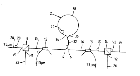
Referring to Figure 1, an optical routing apparatus
comprises a Sagnac loop reflector - often referred to as a
non-linear optical loop mirror (NOLM) - 2 having a first pair
of optical communication ports 4 and 6. The port 4 is
~oupled to a first polarising beam splitter 8 via an optical
fibre 10 into which is spliced a first wavelength
multiplexing coupler 12. The port 6 is similarly coupled to
a second polarising beam splitter 14 via an optical fibre 16
into which is spliced a second wavelength multiplexing
coupler 18.
The polarising beam splitters 8 and 14 may be bulk
optic devices or waveguide devices.
Optical fibres 20 and 22 are optically coupled to the
polarising beam splitter 8 so that vertically polarised
optical signals pass between the fibres 20 and 10, whilst
horizontally polarised optical signals pass between the
fibres 22 and 10.
2078994
-- 5
Similarly, optical fibres 24 and 26 are optically
coupled to the polarising beam splitter 14 so that vertically
polarised signals pass between the fibres 16 and 24, whilst
horizontally polarised signals pass between the fibres 16 and
26.
In this embodiment, an input optical data stream to be
routed is assumed to propagate along the fibre 20 towards the
beam splitter 8. A polarisation controller 28 is used to
ensure the data signal is vertically polarised on entering
the beam splitter 8, so it will be coupled to the loop
interferometer 2. In this embodiment the optical data stream
is at a wavelength of about 1.5~m.
A source (not shown) of an optical signal of about
1.3~m is couplable into the fibre 10 by the wavelength
multiplexing coupler 12.
As will be explained below, transmitted optical
signals from the loop interferometer 2 will be horizontally
polarised on leaving the port 6. Generally, however, their
polarisation will change as they propagate to the beam
splitter 14. A polarisation controller 30 is included near
the beam splitter 14 to adjust the polarisation of the
transmitted optical signals to vertical or horizontal
polarisation depending on which of the fibres 24 and 26 is
chosen as the output fibre for onward transmission of the
data stream. In this case, it is assumed that the fibre 26
is the output fibre, so the polarisation controller 30 is set
to provide horizontal polarisation at the beam splitter 14.
The multiplexing coupler 18 selectively couples out
from the fibre 16 any control optical signal at the second
wavelength of 1.3~m.
The Sagnac loop 2 comprises a dichroic optical coupler
32, constituting a first optical coupling means, the loop
having the ports 4 and 6 as a first pair of ports, and the
ports 34 and 36 as a second pair of ports. The ports 34 and
36 are coupled by a loop of silica optical fibre 38. The
coupler 32 is to be close to 50:50 coupling at 1.5~m and
100:0 at 1.3~m as possible for maximum efficiency and
2078994
-- 6
completeness of switching. The wavelengths chosen for
operation are arbltrary. Others may be used if the couplers
are selected appropriately.
A polarisation controller 40 is positioned close to
the port 34, and set such that an optical signal exiting
either of the ports 34 and 36 will arrive at the other port
in the orthogonal polarisation. The counter-propagating
portions of an optical signal at l.5~m will, in general, have
an arbitrary phase relationship. If the interferometer 2 is
to act as a reflector or as a transmitter, in the absence of
a 1.3~m signal, the relative phase difference should be 0 or
~ radians respectively. In the embodiment of Figure 1, the
polarisation controller 40 can be adjusted to obtain the
required phase relationship.
Consider a stream of optical data signals vertically
polarised at the beam splitter 8. The connection between the
fibre 20 and the beam splitter 8 will be referred to as V1.
The signal will be coupled to the port 4 of the
interferometer 2, and will be reflected out of that port
back to the beam splitter 8. The signal will be horizontally
polarised due to the action of the polarisation controller 40
and the reciprocal propagation conditions of the fibre 10.
This horizontally polarised signal will, therefore, be
connected by the polarising beam splitter 8 to the fibre 22,
which connection is referenced H1.
If a 1.3~m optical control signal is coupled to the
port 4 of the interferometer 2 via the coupler 12, it will
propagate in substantially only one direction round the
interaction section 38 because the coupler 32 is close to a
100:0 coupler at the second wavelength. The intensity is
selected to provide sufficient cross phase modulation between
the control signal and the co-propagating portion of the
1.5~m signal to provide a ~ radian relative phase shift
between the co-propagating portions. The 1.5~m signal, so
effected, will now exit the interferometer at the port 6. As
stated above, this signal is controlled to have a horizontal
polarisation by the polarisation controller 30, and so will
207899~
-- 7
exit the beam splitter 14 to couple to the fibre 26. This
connection is labelled H2. The connection between the beam
splitter 14 and the fibre 24 is labelled V2.
The symmetric nature of the embodiment provides the
following connection pattern for 1.5~m signals, firstly
without the 1.3~m control signal:
V1 ----H2
H1 ----V2
V2 ----H1
H2 ----V1
and secondly with the 1.3~m control signal:
V1 ----H1
H1 ---- V1
V2 ----H2
H2 ----V2
When the optical signal entering the connection V1 of
the Figure 1 embodiment is a stream of optical pulses,
representing binary digits, a drop function can be performed
by applying a control pulse which overlaps the pulse to be
dropped. This pulse will be reflected by the interferometer
2 back to the beam splitter 8 to exit at H1. To perform an
insert function, the pulse to be inserted is coupled to the
interferometer 2 so that it coincides with a control pulse at
the appropriate place in the data stream. The control pulse
will cause the data to be inserted to exit at H2, with the
rest of the data stream which has not been switched by the
control pulse.
The drop function can be used for high bit rate, time
division multiplexing, by applying a sequence of control
pulses to the coupler 12 at a sub-multiple of the line rate.
Packets of data can be dropped if a control signal the length
of several bits is employed.
The embodiment of Figure 1 can be operated in the mode
in which the interferometer 2 is normally reflective in the
2078~94
absence of a control signal, i.e. the polarisation controller
40 is set so that counter-propagating pulses are in phase on
reaching the coupler 32. In this case, the connection
pattern for the presence and absence of a control signal is
the converse of the previously described operation.
Referring now to Figures 2 to 4, there are shown
graphs of the output pulses obtained from the embodiment of
Figure 1 measured after they pass from the coupler 18, in
which the control signals at 1.3~m comprise 130ps pulses from
a Nd:YAG laser, and the input signal to be switched comprises
a pulsed, low power signal from a semiconductor DFB laser
operating at 1.53~m coupled at the port 4.
Figures 2 and 3 show the output of the DFB pulses at
1.53~m from the ports 6 and 4 respectively. That is, the
interferometer loop is set to transmit pulses from the port
4 to the port 6 in the absence of a control signal at 1.3~m.
Figure 4 shows the DFB pulse switched to the port 6 by the
presence of the control signal when the interferometer 2 is
set to operate in reflective mode in the absence of a control
signal.
Figure 2 shows the DFB laser pulse detected when the
Sagnac loop interferometer 2 is arranged to be transmitting
in the absence of the 1.3~m control signal and no control is
present.
Figure 3 shows the effect on the output at Figure 2 of
introducing the 1.3~m control signals to the optical
waveguide. Each fourth pulse is partially reflected by the
Sagnac loop 2. Partial switching of the centre of the 1.53~m
pulses occurs because the control pulse is narrower than the
1.53~m pulses.
Figure 4 shows the DFB laser, 1.53~m, pulses received
after the coupler 18 in the presence of 1.3~m control pulses
when the Sagnac loop 2 is reflective in the absence of the
control signals. In this case all 1.53~m pulses are
reflected except when a control pulse is present.
Figure 5 shows the arrangement of Figure 1 but in
which the waveguide connecting the ports 34 and 36 is a
20789~4
g
polarisation-maintaining fibre 39, and there is a further
polarisation controller 42. The polarisation controllers 40
and 42 are set such that the one portion of an input signal
coupled via the fibre 20 at 1.3~m propagates round the fibre
38 in either the slow or fast axis of the fibre, the other,
counter-propagating portion being in the other axis. The
fibre 38 will then be more able to maintain the portion in
the same polarisation state as the signals propagate round
the fibre 38. One of the controllers 40 and 42 could be
replaced by a polarisation controller ad;acent to the port 4.
A fibre stretcher 44 is attached to the polarisation-
maintaining fibre to provide a means for setting the required
phase difference in the absence of a control signal.
The 1.5~m control signal is inserted and extracted
15 within the Sagnac loop via wavelength multiplexing couplers
46 and 48. The couplers 12 and 18 of Figure 1 are,
therefore, not needed. The operation is as for the Figure 1
apparatus.
Referring now to Figure 6, an optical memory comprises
the embodiment of Figure 1 shown as the optical router 50
with ports V1, H1, V2 and H2. The router 50 is set to be
normally transmitting, ie V1 and H2 are coupled, and V2 and
H1 are coupled. The port H1 is coupled externally to the port
V1 by an optical waveguide 51 via a half-wave plate 52 and an
optical amplifier 54. The half-wave plate 52 ensures optical
signals coupled out from H1 can be coupled into the router 50
in the appropriate polarisation state at V1. A polarisation
controller may be included if necessary. An optical control
signal is applicable via an optical waveguide 56.
In the absence of a control signal, optical signals
coupled to the port V1 will be coupled via the router 50 to
the port H2, and the port V2 will be coupled to the port H1.
When a control signal is present, the input at the port V1
will be switched to the port H1. Thus, if the input to the
35 port V1 is a stream of optical pulses, they can be
selectively switched to the waveguide 51. If the control
signal is removed before a switched pulse reaches the port
rr.
2078994
-
-- 10 --
V2, the switched pulses will be coupled via the router 50 to
the port H1, and so continue to circulate in the loop defined
by the waveguide 51 and the router 50. The amplifier 54
maintains pulse intensity.
Similarly, if the control signal is applied at the
appropriate time, pulses circulating in the loop will be
switched out as the port V2 will be coupled to the port H2.
Other specific arrangements of optical memories will
be realisable employing the present invention.
A further embodiment of the present invention, and the
results of optical pulse switching obtained with it, will now
be described with reference to Figures 7 and 8(a) and 8(c).
The first target is to reduce the switching power
required, so that semiconductor lasers may be used throughout
the device. This can be achieved by increasing the length of
the fibre loop used in the NOLM. The original experiment
employed a 100m loop, which required a peak power of 10 watts
for complete switching. Increasing the loop length will
proportionally reduce the required switching power, but how
far it can be taken depends on, amongst other things, the
stability of the loop for long lengths. In a series of
experiments, we established that, using standard
communications fibre, the loop was stable for a period of
hours for lengths at least up to the loss length of silica.
This means that the NOLM is the first non-linear fibre device
which is capable of accessing the full potential of the
silica non-linear figure of merit (the ratio of non-linear
coefficient to loss). The loop employed in the current
experiment was 6.4km of standard dispersion shifted fibre 70,
and stability measurements showed no significant drift over
an hour. With this loop, the peak power required for
complete switching was approximately 160mW. This means that,
for example, with a 10ps pulse the switching power was only
1.6pJ.
The next problem to address was the provision of a
switching source and a signal source. The two wavelengths
chosen for the experiment were 1.53~m for the switching
2078994
11 --
source and 1.56~m for the signal source. These wavelengths
were chosen to be both within the Er gain window, and to
straddle the dispersion minimum of the fibre 70 to minimise
the group delay difference between the two wavelengths. This
S difference in group delay causes one signal to 'walk through'
_he other signal, so that the effective switching pulse
broadens. Therefore, at high bit rates, it was important to
minimise this difference by ensuring that the wavelengths
were set equally on opposite sides of the zero dispersion
10 wavelength. This condition is easier to satisfy when the
wavelengths are closely spaced, because the group delay
function is slow moving near the zero dispersion wavelength,
thus easing the tolerance requirements of the two
wavelengths. Consequently, the fibre chosen for the loop had
a zero dispersion wavelength at 1.545~m.
The switching signal was generated from a gain
switched DFB laser 72 driven at 2.5 GHz. The resulting
pulses were then compressed using 700m of negative group
delay dispersion fibre 74. The full width half maximum
(FWHM) of the pulses was 27ps when displayed on a fast
photodiode sampling oscilloscope detection system 76.
Deconvolving the detection system response implies a pulse
width of -16ps. These pulses were then amplified using a
diode pumped erbium amplifier, which resulted in an average
output power of 20mW. Even allowing for losses in the
following couplers, this is sufficient power to provide
switching in a 6.4km NOLM.
The signal source was a mode-locked diode laser 78
operating at 1.56~m with a repetition rate of 10GHz. These
pulses were interleaved using a fibre Mach-Zehnder 80 to
produce a 20GHz pulse train. The two wavelengths were then
combined using a WDM coupler 82, and launched into the loop
70. The loop 70 was constructed from a coupler 84 which has
a 50:50 coupling ratio for the 1.56~m signal and 100:0 for
the 1.53~m switching signal. Polarisation controllers 86 in
the loop allowed us to operate the loop either in
"reflecting~ or "transmitting" mode. In reflection mode, the
2078994
- 12 -
loop output was zero for the 1.56~m signal, in the absence of
the switching pulses, and the complete signal was reflected.
The injection of the switching pulses caused the signal
pulses to be switched to the output 88 of the loop 70. In
transmitting mode, the situation was reversed, and the
switched out pulses were reflected. The output of the loop
70 was connected to a filter 90, which passes the 1.56~m
signal and blocks the switching pulses. The remaining signal
was amplified by an erbium fibre amplifier, detected by a
10 photodiode 94, and then displayed on the sampling
oscilloscope
76.
In order to establish the switching of this
configuration, the mode-locked signal source 78 was replaced
15 with a cw source operating at the same wavelength (1.56~m).
The 'effective' width of the switching pulse was determined
by a combination of the difference in the group delay between
the two wavelengths and the initial pulse width. The loop
was set up in the reflecting mode, and the width of the pulse
switched from the cw source was measured as 33ps on the
oscilloscope 76 which deconvolves to 25ps. The initial pulse
width was 16ps, thus indicating a difference in dispersion
between the two wavelengths of 3 ps/km. This established
that, with this set-up, we should be able to demultiplex at
up to 40Gbit. Having established the suitability of the
switching pulse width, the cw source was replaced by the
mode-locked laser 78. In order that switching took place, it
was necessary to synchronise the two trains of pulses. This
was accomplished by having an adjustable delay in one arm of
30 the clock pulses which drive the two sources.
In Figure 8 we show the results. Figure 8(a) shows
the mode-locked, 1.56~m "signal" pulse train at 20 Ghz.
Figure 8(b) shows the switched output with the loop in
'reflecting' mode, that is a transmission of only those
35 pulses coinciding with the switching pulses i.e. every eighth
pulse. Figure 8(c) shows the result when the loop is set up
in the 'transmitting' mode, and clearly shows every eighth
~07sqs4
- 13 -
pulse being switched out. There is still a small residual
component of the switched-out pulse. This is because we may
not be quite at the total switching energy. Increasing the
amplification of the 1.53~m pulses will result in more
complete extinction.
We have shown that the NOLM is capable of switching
multigigabit rates, and have demonstrated stable operation at
the silica loss length (e.g. 6km), allowing ultra-fast, all-
optical processing to be performed entirely with
semiconductor sources. This device is also capable of a
number of non-linear processing functions, including pulse
insertion, wavelength translation, logic and all-optical
memory.