Note: Descriptions are shown in the official language in which they were submitted.
-1-
56,793
PATENT
CTRCUIT BREAKER WITH
PROTECTION AGAINST SPUTTERTNG ARC FAUDTS
BACKGROUND OF '.CHE INVENTION
Field of the Invention
This invention relates to circuit breakers and
more particularly to a ,circuit breaker with an electronic
trip unit which responds to sputtering arc-type faults.
Background Information
Conventional residential circuit breakers have a
thermal trip device which responds to persistent aver-
currents of moderate magnitude to provide a delayed trip and
a magnetic trip device which responds instantaneously to
overcurrents of large magnitude. Thus, the fault current
must reach a predetermined magnitude, fir example, ten times
rated current, for the instantaneous trip to occur, or the
overcurrent must sustain a predetermined average value over
a given time interval to implement the delayed trip.
There as a type of fault, however, which may not
produce either the peak magnitude required for the
instantaneous magnetic trip, or the sustained average over-
current necessary for the delayed trip, yet it may pose a
fire hazard. This is the intermittent or sputtering arc-
typ~ of fault. Such a fault can occur,. for instance,
between two conductors that are in close proximity, but not
touching, so that an arc is struck between the conductors.
This arc can produce a temperature high enough to melt the
copper in the conductor. The melted droplets of copper can
~~'~~:;~.r~a
' ignite flammable materials in the vicinity. However, the
resistance of the wiring rnay be high enough to limit the
peak ourrent and the ac current cyclically passes through
zero to extinguish the arc so that the average current is
low. Thus, the conventional. circuit breaker does not
respond to the fault, although a hazard exists. This is
especially true in the case of a stranded wire extension
cord where an individual strand can be melted at a
relatively low fault current.
As sufficient voltage is required to strike the
arc of a sputtering arc fault, this type of fault typically
occurs at the peak of the ac voltage waveform thereby
resulting in a step increase in current. Switching of some
residential loads also produces step increases in ourrent.
For instance, an iron which is turned on at the peak of the
voltage waveform results in a step inorease in ourrent;
however, the magnitude of the step is less than the rated
current of the circuit breaker. In addition, inrush
currents, such as those produced by the starting of a motor,
also rise rapidly, although not as rapidly as an arc-type
fault. Furthermore, inrush currents tend to decay
exponentially while faults maintain a constant high value,
or drop to zero in the case of a sputtering arc.
There is a need for a circuit breaker which can
respond to a sputtering arc fault.
There is also a need; however, for such a circuit
breaker which can distinguish between acceptable inrush
currents and avercurrents produced by sputtering arc faults.
There is an additional need for such a circuit
breaker which is reliable and economical.
~'' '~ ~ ~'
-3-
SUNIP~AI2Y OF THE INVEN~.CION
These and other needs are satisfied by the
invention which is directed t:o a circuit breaker which
compares a sensed signal representative of current in the
protected circuit to a plurality of threshold levels and
which times the intervals that: the sensed signal remains
above each of these levels, If any of these time intervals
are exceeded, the circuit breaker is tripped. The threshold
levels and timing intervals are selected to approximate,
with a selected margin, a response envelope for generation
of the trip signal which approximates, with a selected
margin, the response of the protected circuit to a selected
inductive load. When the sensed signal falls below a
previously exceeded threshold, the accumulated time that the
sensed signal was above that level is retained, so that if
the overcurrent again reaches that threshold level, timing
is resumed from where it left off. Thus, as in the case of
a sputtering arc fault, where the current can drop off and
rise again, a trip signal will be generated when the total
selected time for that threshold level has been exceeded
even though the current can intermittently fall below that
level. The timing intervals are reset when the sensed
signal falls below the lowest threshold level. Even then,
the intervals are cleared at a very slow rate so that if the
current again exceeds one of the thresholds, the interval
will be shorter before a trip is generated.
HRIEF DESCRIPTION OF THE DRAWINGS
A full understanding of the invention can be
gained from the following description of the preferred
embodiments when read in conjunction with the accompanying
drawings in which:
-4-
Figure 1 is a schematic diagram of a circuit
breaker in accordance with the invention shown in relation
to a protected electric circuit.
Figure 2 is a schematic circuit diagram of one
embodiment of a detector circuit which forms a part of the
circuit breaker shown in Figure 1.
Figure 3 is a schematic circuit diagram of another
embodiment of the detector circuit which forms a part of the
circuit breaker shown in Figure Z.
l0 ~ DESCRIPTION OF THE PREFERRED EMBODTMENTS
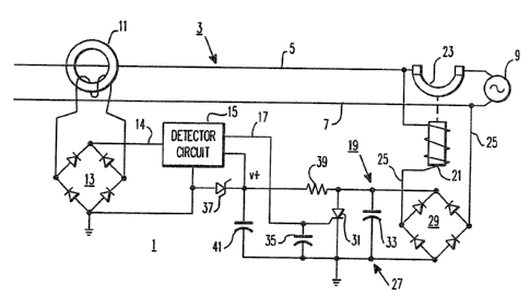
Figure 1 illustrates a circuit breaker 1 in
accordance with the invention for protecting a one phase
electrical system 3 which includes a line conductor 5 and a
neutral conductor 7 energized by a 60 Hz source 9. The
circuit breaker l includes a sensor 11 for sensing current
in the line conductor 5. Preferably, the sensor 11 is a
di/dt sensor which senses the rate of change of the current
in the line conductor 5. A suitable di/dt sensor is a
mutual inductor having a low permeability core, such as an
air core or a pa.wdered iron core. The sensed di/dt signal
is full wave rectified in the bridge circuit 13 with the
resultant pulsed do signal applied to a detector circuit 15
through lead 14 connected to the do terminals of bridge
13. As will be more fully discussed below, the detector
circuit l5 compares the rectified sensed signal to a number
of reference signals and times the intervals that the sensed
di/dt signal remains above each of these thresholds. If the
rectified di/dt signal remains above any of the reference
signals for the associated interval, a trip signal is gen-
crated on a lead 17 which is connected to a trip circuit 19.
The trip circuit 19 includes a trip solenoid 21
which when energized opens circuit breaker contacts. 23 to
~~ ,~ r .i ~
6~"t~ ~~.~ C~l~
_g_
disconnect the protected portion of the electrical system 3
from the ac source 9. The trip solenoid 21 is energized
from the protected electrical system 3 through lead 25 and
is controlled by control circuit 27 which is energized by a
bridge circuit 29 connected in series with the trip solenoid
21 by the lead 25.
The control circuit 27 includes a silicon
controlled rectifier (SCR) 31 connected across the do
terminals of the bridge 29. The gate of the SCR 31 is
connected to the lead 17 from the detector circuit 15.
Capacitors 33 and 35 protect the SCR from high frequency
spikes.
A zener diode 37 energized by bridge 29 through
current limiting resistor 39 generates a V+ reference
voltage for the detector circuit 15. Capacitor 41 is a
filter.
When the circuit breaker is closed closing the
contacts 23, the capacitor 33 charges. This charging
current is insufficient to energize the trip solenoid 21.
2'0 Current drawn by the V+ supply is also insufficient to
generate a trip. With the capacitor 35 charged and the SCR
31 off, no appreciable current flows through the trip
solenoid 21, and hence, the electrical system 3 remains
connected to the ac source 9. When the detector circuit 15
generates a trip signal on the lead 17, the SCR 31 is turned
on providing a law resistance path for current which is
sufficient to energize the trip solenoid 21 to open the
contacts 23. Opening of the contacts 23 deenergizes the
trip circuit 19, however, the circuit breaker contacts 23
remain open until reset.
~~ ~fi.~.~ia
_6_
An analog implementation of the detector circuit
15 is illustrated in Figure 2. Tn the detector circuit 15,
the full wave rectified sensed di/dt signal provided on lead
14 is filtered by an RC filter comprising resistor 43 and
capacitor 45. A plurality of level detectors (three in the
exemplary embodiment) in the form of comparators 47, 49 and
51 compare the filtered do di/dt signal to a plurality of
reference voltages. The sensed signal is applied to the
non-inverting inputs of the comparators 47, 49 and 51
through input resistors 53, 55 and 57. respectively. The
reference voltages which are applied to the non-inverting
inputs of the comparators are generated by a voltage divider
which includes resistors 59, 61, 63 and 65 connected in
series between the regulated voltage supply V+ and ground.
Feedback resistors 67, 69 and 71 are selected to provide a
positive feedback or hysteresis in an amount greater than
the magnitude of the ripple on the capacitor 45. Indicators
in the form of LED's 73, 75 and 77 are turned on to provide
a visual indication when the sensed di/dt signal exceeds the
reference voltages applied to the comparators 47, 49 and 51,
respectively. k~esistors 79, 81 and 83 limit current through
these LED's.
The output of the comparator 47 is applied through
a diode 85 to a timer 87 formed by the series connected
resistor 89 and capacitor 91.
The output of comparator 49 is applied through AND
gate 93 and diode 95 to a timer 97 which includes resistor
99 and capacitor 101. The AND gate 93 is controlled b~ the
output of the comparator 47 through inverter 103.
Similarly, the output of the comparator 51 is applied
through AND gate 105 and diode 107 to a timer 109 which
includes a resistor 111 and capacitor 113. The AND gate 105
is controlled by the outputs of both the comparators 47 and
~~"~~~.~;?
_7_
49 through NOR gate 115.
The voltages across flee capacitors 91, 101 and 113
are applied through diodes 117, 119 and 121, respectively,
and across a resistor 123 to the non-inverting input of a
comparator 125 having a threshold voltage applied to its
inverting input by a voltage divider comprising the
resistors 127 and 129 and energized by the regulated voltage
V+. Each of the capacitors 9l, 101 and 113 is also
connected through a diode 131, :L33 and 135, respectively, to
a discharge resistor 137. The outputs of each of the
comparators 47, 49 and~51 are ORed in OR gate 143, the
output of which is connected to the discharge resistor
137. A resistor 139 and an LED 141 are connected from the
output of the OR gate 143 to ground.
The operation of the detector circuit 15 of Figure
2 is as follows. The level of the sensor signal supplied on
the input lead 14 is continuously compared with the
reference values in the comparators 47, 49 and 51.~ The
outputs of the respective comparators are time delayed by
the timers 87, 97 and 109; however, at any given time only
the output of the comparatar associated with the highest
reference voltage which is exceeded is passed through to the
respective timer. Thus, if the sensor signal exceeds the
reference applied to the comparator 47, AND gate 93 is
inhibited through inverter 103 to block timing of the output
of comparator 49 and AND gate 105 is disabled through NOR
gate 115 to inhibit timing of the output of comparator 51.
When the delay selected by the timer 87 has expired so that
the voltage across the capacitor 91 minus the forward drop
of diode 117 exceeds the reference voltage applied to
comparator 125, a trip signal is generated on the output
lead 17.
t /~ F~ ~ a57 S
~Y ~ 2~ 17..
.$.
If the sensor signal falls below the threshold of
comparatar 47 before a trip signal is generated, but remains
above the threshold of comparator 49, AND gate 93 is enabled
and timer 97 begins timing out. If the sensor signal
remains above the threshold of comparatar 49 for the
selected time interval, the comparator 125 will generate a
trip signal.
If the sensor signal falls below the threshold of
comparator 49 before the timer 97 times out, but remains
above the threshold of comparator 51 AND gate 105 is enabled
by NOR gate 115 and the ~ timer 109 is activated. Again, i.f
this timer times out, a trip signal is generated by the
comparator 125.
The delay accumulated in the respective timers is
retained as Lang as the sensor signal remains above the
threshold of any of the comparators 47, 49 or 51. This is
implemented by the OR 143 which raises the voltage at the
junction between the resistors 137 and 139 to prevent
discharge of the capacitors 91, 101 and 113 of the timers.
Thus, if the level of the sensor signal rises again above
the threshold of a higher level comparator, the associated
timer picks up timing at the point where it left off, and a
trip signal will be generated when the accumulated elapsed
time set by the timer has expired. When the sensor signal
falls below the threshold of the comparator 51, the timer
capacitors are discharged through the resistor 137. The
resistor 137 is selected so that the discharge time constant
is much larger than the charging time constant so that if
overcurrent conditions return, a trip will be generated
sooner than for an initial overcurrent condition. The LED's
73, ?5 and 77 are turned on when the thresholds of the
associated comparators have been exceeded. This provides a
visual indication that an overcurrent condition exists which
1~~~~~~~w~ ~r
-9-
could result in a trip and the relative severity of the
overcurrent. The LED 141 provides a redundant indication,
when it is energized, that overcurrent conditions exist.
Alternatively, only the LEDs 73, 75 and 77 or just the LED
41 could be pravided.
The threshold reference voltages of the
comparators 47, 49 and 51 and the time constants of the
timers 87, 97 and 109 are selected to generate an envelope
which approximates the exponential decay of a step
function. This envelope can be set so that it exceeds, but
follows, the response which would be generated by the intro-
duction of an inductive load, such as the starting of a
motor, in the electrical system 3 protected by the circuit
breaker. Thus, the circuit breaker would not trip on the
starting of the motor, but would provide short delay
response for faults, and would be especially useful for
respanding to low overcurrent but persistent faults such as
sputtering or intermittent arc faults.
Figure 3 illustrates a hybrid analog/digital
implementation of the detector circuit. Components in this
detector circuit 15° which are identical to components in
the analog circuit of Figure 2 are identified by like
reference characters. This circuit 15' includes digital
delay or timer circuits S7', 97', and 109', respectively,
associated with the comparators 47, 49 and 51, respectively.
The timers 87°. 97' and 109' each include an
up/down counter 145, 147 and 149, respectively. Each of the
counters 145, 147 and 149 have the number of stages required
for the respective time delays. The output of the
comparator 47 is applied through an APID gate 151 to the
count-up input of the counter 145. Similarly, the outputs
of comparators 49 and 51 are applied to the count-up inputs
~v~a~~~~.~irj
-l0~
of the counters 147 and 149, respectively, through the AND
gates 93 and 105. These AND gates are enabled by clock
pulses. The clock pulses are generated from the 60 Hz of
the electrical system 3 by a Schmitt trigger 153. Since the
delay intervals are long compared with the period of the 60
Hz of the electrical system, the pulses generated by the
Schmitt trigger 153, are divided down by a factor of K by
divider 155. The last stages of the counters 145, 147 and
149 are ORed by OR gate 157 to generate the trip signal. on
lead 17 when any of the counters times out.
As in the case of the circuit of Figure 2, only
the counter in the circuit 15' associated with the
comparator having the highest threshold which is exceeded
counts at any given time. The counters 145, 147 and 149 are
reset by clock pulses from divider circuit 159 which divides
the clock pulses down further by a factor of M so that the
'counters are reset at a slower rate than that at which they
count up. The reset pulses from the divider 159 are applied
through AND gates 161, 163 and 165 to the count-down inputs
of the counters 145, 147 and 149, respectively. These AND
gates 161, 163 and 165 are enabled by outputs from OR gates
167, 169 and 171 which OR the bits of the associated
counters. Thus, the AND gates 161, 163 and 165 pass pulses
from the divider 159 to the count--down inputs of the
counters 145, 147 and 149 until the counts reach zero. The
OR gates 167, 169 and 171 prevent the counters from rolling
over after they reach zero. Reset pulses are generated by
the divider 159 only when none of the thresholds of the
comparators 47, 49 or 51 are exceeded as .determined by the
OR gate 143 which holds the divider 159 at reset as long as
a threshold of one of the comparators 47, 49 or 51 is
exceeded. If desired. indicators such as the LEDs 73, 75
and 77 or the LED 141 can be included in the detector
CA 02079182 2001-12-21
-11-
circuit 15' to provide a visual indication of the level of
the overload current or to generally indicate an overload
condition.
The electronic trip feature of the invention can
be incorporated into a conventional circuit breaker having a
magnetic instantaneous and a delayed thermal trip, such as
the circuit breakers disclosed in United States patent Nos.
3,858,130; 3,999,103 or 4,081,852. The present
invention provides protection against
faults such as sputtering arc faults in
which the overcurrent is less than that required for an
instantaneous magnetic trip, but greater than that required
for a thermal trip. The additional components required by
the invention are housed in the half of the circuit breakers
of these patents housing the trip solenoid, and are
connected to the trip solenoid which when energized rotates
a lever extending through a partition to actuate the trip
mechanism in the other half of the housing.
While specific embodiments of the invention have
been described in detail, it will be appreciated by those
skilled in the art that various modifications and alter-
natives to those details could be developed in light of the
overall teachings of the disclosure. Accordingly, the
particular arrangements disclosed are meant to be illustra-
tive only and not limiting as to the scope of the invention
which is to be given the full breadth of the appended claims
and any and all equivalents thereof.