Note: Descriptions are shown in the official language in which they were submitted.
JA9--91-034 2 0 7 9 3 5 2
DISPLAY SYSTEM
This invention relates to a display system for converting gray
levels of a display device and, more particularly, to a display
system for converting N bit signal representing 2N gray levels (N
being an integer larger than or equal to 2), to M bit signal
representing 2 gray levels (M being an integer satisfying
N>M21).
Brie~ Description of the Drawings
The invention will be more clearly appreciated and understood
~rom the following description taken in conjunction with the
appended drawings wherein:
Fig. 1 is a block diagram of a display sytem in accordance
with the present invention;
Fig. 2 is a block diagram of a configuration of the display
system;
Fig. 3 shows the number of horizontal and vertical dots and
aspect ratio of various display devices;
Fig. 4 is a flow chart of one embodiment of the present
invention;
Figs. 5, 6, and 7 illustrate dot patterns generated in
accordance with the present invention;
Fig. 8 is a flow chart of another embodiment of the present
invention;
Fig. 9 illustrates a dot pattern generated through the
invention as per Fig. 8;
Fig. 10 illustrates one example of an alternate table;
Figs. 11, 12, 13 and 14 respectively illustrate dot patterns
generated by the prior art.
Background of the Invention
In the prior art, it has been required to connect two display
device, such as CRT (Cathode Ray Tube) display device and LCD
JA9--91--034 . 2 0 7 9 3 5 2
(Liquid Crystal Display) device to a personal computer. Such
configuration is shown in Fig.2, wherein an output of a personal
computer 20 is connected to the CRT display device 21 and the LCD
device 25 through a digital-analog converter 22 and a LCD
controller 23, respectively. Gray levels displayed by the two
display devices differ from each other. For example, the CRT
display device 21 displays 64 gray levels and the LCD device 25
displays 16 gray levels. The personal computer 20 supplies 6 bit
signal for each picture element of the display devices on the
output line. The 6 bit signal represents the 64 gray levels of
the CRT display device 25. It was required to display the 64
gray levels on the LCD device 25, each pel of which displays only
the 16 gray levels. To this end, the LCD controller 23 responds
each 6 bit signal to generate four 4 bit signals. The 4 bit
signal represents the 16 gray levels displayed by one pel of the
LCD device 25. And, four pels of the LCD device 25 are used to
display the four 4 bit signals, so that if a size of one image
supplied from the personal computer 20 is 320x200 pels (dots),
the CRT display device 21 has 320x200 dots and the LCD device 25
has 640x400 dots, as shown in Fig.3. The controller described
above is disclosed in Japanese patent application 63-236291
corresponding to US Patent 5059962, assigned to the same assignee
as that of the present application. Blocks assigned with
reference number 1, 2, 3, 4, 5, 6, 7, 8, 9, 10, 12, 21 and 25 in
Fig.1 show the controller of the Japanese patent application 63-
236291. Detail operation for generating the four 4 bit signals
for the LCD device 25 based upon one 6 bit signal for one pel of
the CRT display device 21 will be described hereinafter since the
present invention also uses the algorithm of the Japanese patent
application 63-236291.
Summary of the Invention
The invention is a display system for converting N bit signals,
each representing 2N gray scale levels, to M bit signals
representing 2M gray levels, where N is an integer larger than or
equal to 2 and M is an integer satisfying N>M21. The system
JA9-91-034 2a 2079352
comprises: means for separating each of the bit signals into
higher M bits and N-M bits, 2N M tables which each store a
distinctive set of PxQ modification values satisfying PxQ22
the means for selecting one of the tables using the N-M bits,
means for detecting unequality between a first set of
modification values and a second set of modification values of
the selected table, means for exchanging the first set of
modification values and the second set of modification values to
generate a modified table of the selected table, means for adding
the M bits of one N bit signal and each of the modification
values of the selected table to generate a first set of PxQ M bit
signals, and for adding the M bits of the next N bit signal and
each of the modification values of the modified table to generate
a second set of PxQ2M bit signals, and means for supplying the
first and second sets of M bit signals to a display device of 2M
gray levels. The invention also includes a method of converting N
bit signals using the novel display systems.
Detailed Description of the Preferred Embodiments
The present invention solves a problem encountered in trying to
use the algorithm for displaying the image on the LCD display 25.
It is assumed that the Dx dots of the CRT display device 21 is
equal to 320 dots, and the Dy dots is equal to 200 dots. Since
one pel displayed by the CRT
JA9-91-034 3 20793~2
display device 21 is displayed by four pels of the LCD
device 25, 640 dots in the X direction and 400 dots in the Y
direction are required in the LCD device 25, as shown in
Fig.3.
An aspect ratio of the image displayed on the CRT display
device 21 is fixed as A:~. A vertical scanning speed of an
electron beam of the CRT disp]ay device 21 is, which
determines a pitch between the horizontal scanning lines,
controlled to repeatedly display the same horizontal image
dots on two horizontal scan lines. That is, 200 x 2 = 400
horizontal scan lines are displayed within the size B of the
CRT display device 21. This control is made by adjusting
the values of capacitors coi]s and resistor in the CRT
deflection circuit. In contradistinction to the CRT display
device, a pitch between pels of the LCD device is determined
at its fabrication. In the most cases, the aspect ratio C:D
of the displayed image area of the LCD device 25 differs
from the aspect ratio A:B of the displayed image area of the
CRT display device 21, whereby the image displayed on the
LCD device 25 is compressed or stretched in the vertical
direction in comparison with the image displayed on the CRT
display device 21.
To solve the problem, the inventors of the present invention
has tried to use a LCD device having 640 dots in the
horizontal direction and 480 dots ;n the vertical direction,
as shown in the Fig.3~ to disp]ay the image of the same
aspect ratio as that of the CRT display device, i.e. A:B =
E:F. The pitch of the LCD device of 640x480 dots is equal
to that of the LCD device of 640x400 dots. To realize A:B =
E:F, one horizontal image line was added or inserted every
five horizontal image ]ines, and the same image as that of
the just preceding image line is repeatedly displayed on the
added line. But, the inventors of the present invention
have found new problem raised by the addition of the lines.
Before, describing the ne~ problem, the algorithm of the
Japanese patent application 63-236291 is described since the
new problem raises by the combinational use of the algorithm
and the addition of the lines.
JA9-91-034 4 2079352
....
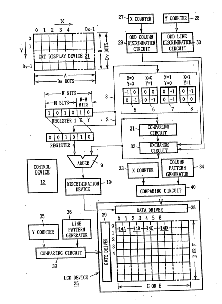
With refer to the Fig.l, t~Je blocks 1, 2, 3, 4, 5, 6, 7, 8,
9, 10, 12, 21 and 25 are the blocks of the Japanese patent
application 63-236291, as described hereinbefore. The
purpose of the algorithm of the patent application is to
respond one 6 bit signal for one pel, such as pel (0, 0), of
the CRT display device 21 to generate four 4 bit signals for
displaying 4 dot image on the four pels of an area 14A of
the LCD device 25.
It will be assumed, for purpose of the description, that the
control device 12 generates a gray level signal, i.e. 6 bit
signal, 101010 (decima] value 42). whlch signal is stored in
the register 1. Next, the contro] device 12 supplies the
higher 4 bits, i.e. M bits, 1010 of the 101010 signal into
the lower 4 bit positions of -the register 4 through the line
2. The higher 2 bit positions of the register 4 are always
0 0. The reason for concatenating the higher 2 bits in the
register 4 will be described below. The control device 12,
on the line 3, supplies the lower 2 bits, i.e. N-M bits, of
the gray level signal 101010 as an address to select one of
the Tables 5, 6, 7 and 8, called as dither matrix. The
number of tables used is determirled by 2N M, so that 4
tables are prepared. The lower 2 hits are represented by x
and y in Fig.l. Where~ N is an integer larger than or equal
to 2 and M is an integer satisfying N>M 1. Since x=l and
y=0, the Table 7 is selected Each table stores 4
modification values, i.e. Px~, satisfying PxQ>2N M and each
distinctive set of modification va]lles corresponds to 4 dots
of each of the area 14A, 14B, 14C, 14D, etc. in the LCD
devices 25. The modification values are represented in
Fig.1 by their decimal values, but as 0 corresponds to the
binary value 00000 and 1 corresponds to the binary value
00001, these binary values are actually stored in the
tables. Any value in the range from +15 to -15 is used as
the modification value. From the viewpoint of fidelity, the
preferred range is +3 to -3. The modification value has 5
bits representing +15 to -15, and a negative value is
represented by the comp]ement of 2. A single higher bit is
concatenated to the 5 bits from the table by a sign
extension. For example, in the case where the modification
value is +1, 00001 is stored in the table, and 0 is
JA9-91-034 5 2 0 7 9 3 S 2
concatenated to the 00001 by the sign extension, so that the
input to the adder 9 from the table is 000001. In the case
where the modification value in the table is -1, 11111 is
stored in the table, 1 is concatenated to the 11111 by the
sign extension, so that 111111 is supplied to the adder 9.
Since the input to the adder ~ from the tables is 6 bits,
the input from register 4 is also made to be 6 bits, so that
it will be seen why the 2 leading 0 bits are concatenated in
the register 4.
To generate a gray level signa] for the dot (0, 0) of the
area 14A of the LCD device 25, the control device 12 first
concatenates the bit 0 to the upper left modification value
00000 in the Table 7, and supplies the 000000 to the adder
9.
Next, the control device 12 activates the adder 9 to add
both the inputted bits from the Table and from the register
4. That is, the 000000 representing the upper left
modification value 0 in the Table 7 is added to the 001010
(2+M bits), and the total value 001010 is generated.
The control device 12 operates to supply the total value
001010 to the discriminaticn device 10. The discrimination
device 10 generates a signal on the output line in
accordance with the tota] value received. In particular,
de~-ice 10 generates a signal corresponding to the value 15
(binary value 1111~ on the output line, if the total value
is larger than 15; generates 0 (binary value 0000) on the
output line, if the total value is smaller than 0, that is,
the total value is a negative value; and supplies the lower
4 bits of the total value on the output line, if the total
value satisfies 15 ~ total value ~ 0. To perform the
discrimination, the upper 2 bits of the total value are
determined or tested. When the most significant bit of the
total value is 1, it indicates that the total value is
negative. When the value of the higher 2 bits of the total
value is 01, it indicates that the total value is larger
than 15, and when the val~e of the higher 2 bits of the
total value is 00, it indicates that the re]ation 15 2 total
value ~ 0 is satisfied. In the case of the upper left
JA9-91-034 6 2079~2
modification value in the Table 7, the total value is
001010, so that the 4 bits 1010 are supplied to the LCD
device 25 as the gray level signal for the dot (0, 0) in the
area 14A, whereby a gray level of 10 (i.e. binary value
1010) is displayed at the dot (0, 0) of the display device
25.
Next, in order to generate a gray level signal for the dot
(1, 0) in the area 14A of the display device 25, the control
device 12 reads out the upper right modification value 1
(binary value 00001) in the Table 7~ converts it to the 6
bits 000001 by the sign extension~ supplies those 6 bits to
the adder 9 and supplies the 6 bits 001010 in the 2+M
register 4 to the adder '~. Next~ both of these values are
added. The total value is 0010]1 and it satisfies 15 2
total value ~ 0~ so that the bits 1011 are supplied to the
LCD device 25 as the gray leve] signal for the dot (1, 0) in
the area 14A, whereby a gray ].eve] of 11 (binary value 1011)
is displayed at the dot (1, 0) of the display device 25.
The control device 12 performs the level conversion
operation for the second dot ~1~ 0) in the dot line 0 of the
CRT display device 21~ in the same manner, whereby the gray
level signals for the dots (2~ 0) and (3, 0) in the area 14B
of the LCD device 25 are generated and these dots are
displayed. Similarly~ the third dot and subsequent dots in
the dot line 0 of the display device 2] may be converted,
and two dots in the area 14C and the subsequent areas may be
displayed. In this manner~ the same image may be displayed
on both of the display devices 21 and 25, while the number
of gray levels and the numker of dots of the display device
21 differ from that of the display device 25. As desired,
both devices may be operated simultaneously or the display
device 25 may be operated, while the display device 21 is
not operated, and vice versa.
The gray level signals for the dots of the line 2 of the LCD
device 25 are generated in the same manner. In this case,
the lower left modification value 0 and the lower right
modification value -1 are used to generate the gray level
JA9-91-034 7 2 0 7 9 3 ~ 2
signals for the dots (0, 1) and (1, 1) on the line 1 of the
LCD device 25.
In this manner, the same image as that of the CRT display
device 21 is displayed on the LC~ device 25 of 640x400 dots,
i.e. the aspect ratio of C:D, shown in the Fig.3. However,
the aspect ratio C:D is not equal to A:B of the CRT display
device 21. Then, one horizontal image line was added every
five horizontal lines to display the image of the aspect
ratio of E:F(=A:B) on the LCD device of 640x480 dots shown
in the Fig.3. Figs.ll-14 show the results of the addition of
the horizontal line. In these Figs.11-14, the leftmost 4x4
dot matrix shows the dither matrix tahles 5-8 in the Fig.1,
the middle images show the image dots for the LCD device of
640x400 dots generated by the Japanese patent application
63-236291, and the rightmost images show the images for the
LCD device of 640x480 dots generated by adding or inserting
the new line.
Although the sum of the value (M bits) and the modification
value of the tables is displayed in each pel of the LCD
device, only the modification values are shown in the
Figs.11-14, since the value (M dots) is considered as a
constant value.
The new problem raised by the llSe of the tables 5, 6, 7 and
8 and the addition of the horizon-tal line is, as follows.
The four tables 5, 6, 7 and 8 of 2x2 dots are called as the
dither matrix to display four gra~ levels specified by the
bits X and Y (M-N bits) in the register 1 in the Fig.l.
When human eyes look the 2x2 dither dot pattern, the human
eyes recognize the 2x2 dots of the dither image as a single
pel.
Reviewing the middle dot pattern of the Figs.11-14 from the
above viewpoint, all the middle dot patterns give the human
eyes natural or smooth gray level since a sum of gray levels
of any 2x2 dot matrix in all the middle dot patterns has the
same value. That is, a sum of gray levels of any 2x2 dot
matrix of the middle dot image in the Fig.ll is a value -2,
JA9-91-034 20793~2
similarly, the sum in the Fig.12 is a value -1, the sum in
the Fig.13 is a value 0, and the sum in the Fig.14 is a
value +1.
However, it has been found by the inventors of the present
invention that when one horizontal dot line 2 having the
same dot pattern as that of the just preceding dot line 1 is
added or inserted, as shown in the rightmost dot patterns of
the Figs.11-14, an image line of different gray level from
the remaining portion is observed by the human eyes in the
case of the Figs.12-14.
Referring to the Fig.ll, the sums of gray levels of two dot
lines 0 and 1, 1 and 2, 2 and 3, and 3 and 4 of the
rightmost dot image are equal to the value -8, that is all
the sums are equal to each other, so that the rightmost dot
image with the added dot line 2 is observed as a smooth gray
scale image by the human eyes.
Referring to the sums of the gray levels of two dot lines 1
and 2 in the Figs.12-14, the sum of the two dot lines 1 and
2 differ from the sums of the remaining two dot lines 0 and
1, 2 and 3, 3 and 4, whereby the two dot lines 1 and 2 are
observed by the human eyes as one ;mage line a gray level of
which differs from the remaining portion. Such image line
degrades a quality of the displayed image.
A display system of the present invention for converting N
bit signals each, representing 2M gray levels, to M bit
signals representing 2M gray levels, where N is an integer
larger than or equal to 2 and M is an integer satisfying
N>M>l, comprises: means for separating each of the N bit
signals into higher M bits and lower N-M bits; 2N tables
each of which stores a distinctive set of PxQ modification
values satisfying Px~ 2N M: means for selecting one of the
tables using the N-M bits; means for detecting unequality
between first set of modification values and second set of
modification values of the selected table, means for
exchanging the first set of modification values and the
second set of modification values to generate a modified
table of the selected table; means for adding the M bits of
JA9-91-034 9 2079352
one N bit signal and each of the modification values of the
selected table to generate first set of PxQ2M bit signals
and for adding the M bits of next N bit signal and each of
the modification values of the modified table to generate
second set of PxQ2M bit signals; and means for supplying the
first and second sets of M bit signals to a display device
of 2M gray levels.
The display device receives the first and second sets of PxQ
M bit signals to display them on Q image lines and the same
image as that of the Qth image line on one additional line.
A method of the present invention for converting N bit
signals each, representing 2N gray levels, to M bit signals
representing 2M gray levels, where N is an integer larger
than or equal to 2 and M is an integer satisfying N>M21,
comprises the steps of: separating each of the N bit signals
into higher M bits and lower N-M bits; creating 2N M tables
each of which stores a distinct set of PxQ modification
values satisfying PxQ22N ; selecting one of the tables
using the N-M bits; detecting unequality between first set
of modification values and second set of modification values
of the selected table; exchanging the first set of
modification values and the second set of modification
values to generate a modified tab]e of the selected table;
adding the M bits of one N bit signal and each of the
modification values of the selected table to generate first
set of PXQ2M bit signals and addinq the M bits of next N bit
signal and each o~ the modification values of the modified
table to generate second set of PxQ2M bit signals; and
supplying the first and second sets of M bit signals to a
display device of 2M gray levels.
The first set of modification values in the table are P
modification values arranged in first horizontal line in the
table, and the second set of modification values in the
table are P modification values arranged in second
horizontal line in the table.
The first set of modification values in the table are Q
modification values arranged in first vertical column in the
JA9-91-034 10
207~2
. .
table, and the second set of modification values in the
table are Q modification values arranged in second vertical
column in the table.
Referring to the Fig.l, an embodiment in accordance with
present invention is shown.
Describing the operation of the embodiment of the Fig.l with
refer to a flow chart of Fig.4, the operation starts at the
pel position (O, O). The control device 12 initially resets
the registers 1 and 4, X counter 27, Y counter 28 and Y
counter 35. And, the control device 12 operates an odd
column discrimination circuit 29, a line pattern generator
36 and a comparing circuit 37 since, in this case, the
horizontal lines of the LCD device 25 are added or inserted.
The invention solves the problem described hereinbefore
raised by the dither tables 6, 7 and 8. It is assumed that
the 6 bits signals for all the pels on the pel lines O and 1
of the CRT display device 21 is 101010. The 6 bit signals
are supplied from a data processing device, such as the
personal computer 20.
Operation A:
The operation starts at a block 41. The control device 12
stores the 6 bit signa], i.e. 101010 for the pel position
~O, O) of the CRT displa~ device ~] in the register 1, and
selects one of the dither tables, i.e. the table 7, in a
block 42.
The operation proceeds to a block 43, which determines
whether the addition of the horizontal line, i.e. the line 2
of the rightmost image pattern in the Fig.5, is required.
If the answer is NO, the operation proceeds to a block 47.
In this case, the answer is YES, the operation proceeds to a
block 44, which determines whether the sum, i.e. the value
+1, of the upper 2 values of the dither table 7 is equal to
the sum, i.e. the value -1, of the lower 2 values of the
table 7. The comparing circuit 31 performs the operation of
the block 44. If the answer is YES, the operation proceeds
JA9-91-034 11
20793~2
to the block 47. In this case~ the answer is NO, then the
operation proceeds to a block 45~ which determines whether
the 6 bit signal is used for the odd column pel of the CRT
display device 21. The odd column discrimination circuit 29
performs the operation of the block 45. If the answer is
YES, the operation proceeds to a block 46. In this case,
the pel position (O, O) is located in the even column~ the
answer is NO, then the operation proceeds to the block 47,
which performs the operation of the adder 9 and the
discrimination device 10~ described hereinbefore, whereby
the gray levels~ i.e. O and ~ of the upper two pels (on
the dot line O) in the area 14A of the rightmost pattern of
the ~ig.5 are generated.
Operation B:
Next, the gray level signals of the upper two pels of the
area 14B of the rightmost pattern in the Fig.5, which are
located on the line O are generated, as follows.
The X counter 27 is advanced to the value 1. Therefore, the
control device 12 stores the 6 bit signal 101010 of the pel
position (1, O) in the register 1. And, the operation
starts from the block 41. In the block 42, the dither
matrix 7 is selected, and the operation proceeds to the
block 43 which generates the answer YES. And, in the block
44, the sum, i.e. the value +1~ of the upper two values in
the table 7 are compared to the sum~ i e. the value -1, of
the lower two values in the tab]e 7. Since the answer of
the block 44 is NO, the operation proceeds to the block 45,
which determines whether the 6 bit signa] is being used for
the odd column of the CRT display device 21. In this case,
since the pel position (1, O) is in the odd column, the
answer of the block 45 is YES That is, the odd column
discrimination circuit 29 generates an output signal for
activating an exchange circuit 32. The operation proceeds
to the block 46~ which exchanges the upper two values O and
+1 of the table 7 and the lower two values O and -1, as
shown in the Fig.5. The operation proceeds to the block 47.
In the block 47~ the gray levels O and --1 of the upper two
JA9-91-034 12 2073352
pels (on the dot line O) ln the area 14B of the rightmost
pattern of the Fig.5 are generated.
Operation C:
To generate the gray level signals of the upper two pels of
the area 14C of the rightmost pattern in the Fig.5, the X
counter 27 is advanced to the value 2, and the control
device 12 stores the 6 bit signal 101010 of the pel position
(2, O) of the CRT display device 21 in the register 1. And,
the similar operation as the operation A is performed. It
is however noted that, in this case, the answer of the block
4S is NO, so that the exchange of the values of the table 7
in the block 46 is not performed. And, the gray level
signals O and +1 for the upper two pels of the area 14C are
generated.
Operation D:
To generate the gray level signals of the upper two pels of
the area 14D of the rightmost pattern in the Fig.5, the X
counter 27 is advanced to the value 3, and the control
device 12 stores the 6 bit signa] 101010 of the pel position
(3, O) of the CRT display device 21 in the register 1. And,
the similar operation as the operation B is performed. It
is noted however that, in this case, the answer of the block
45 is YES, then the exchange of th~ values of the table 7 in
the block 46 is performed. And, the gray level signals O and
-1 for the upper two pels of the area 14D are generated.
In this manner, the 6 bit signals of the pels of the pel
line O for the CRT display device 21 supplied from the
personal computer or data processing device 20 are
sequentially stored in the register 1 and sequentially
processed by the algorithm of the Fig.4 to generate the gray
level signals for the pels on the pel line O of the LCD
device 25. The gray level signals are supplied to the data
driver 38 of the l,CD device 25 for displaying the image on
the line 0.
JA9-91-034 13 2 0 7 9 3 52
Next, the gray level signals for the pels of the line 1 of
the LCD device 25 are generated, as follows. Since the 6
bit signals for the pels on the line 0 of the CRT display
device 21 are used to generate the gray level signals for
the pels on both the lines 0 and 1 of the LCD device 25, the
above 6 bit signals for the pels of the line 0 of the CRT
display device 21 are again sequentially processed by the
algorithm of the Fig.4.
It is noted however that the lower two values of the tables
7 and 7A is used to generate the gray level signals of the
pels of the line 1 of the LCD device 25. That is, the lower
two values 0 and -1 of the table 7 are used for the even
areas 14A and 14C, and the lower two values 0 and +1 of the
table 7A, which is exchanged for the values 0 and -1 are
used for the odd areas 14B and 14D.
Next, the line 2 is added after the line 1 of the right most
pattern of the Fig.5. To this end, when the gray scale
signals of the dot on the line 1 of the LCD device 25 is
supplied from the data driver 38 to the LCD cells (or pels),
gate lines 1 and 2 are simultaneously activated by a gate
driver 39. To perform the operation, Y counter 35, a line
pattern generator 36 and a comparillg circuit 37 are
provided. The Y counter 35 is initially reset to the value
0, and advanced to value 1, 2, 3, .. by the control device
12. The control device 12 initial1y stores in the line
pattern generator 36 the values ], 6, 11, ..., which
indicate the lines after which one new line is added. The
comparing circuit 37 compares the value of the Y counter 35
with the value of the line pattern generator 36. If both
the values are equal, the comparing circuit 37 supplies a
signal to the gate driver 39. The gate driver 39
sequentially activates the gate lines, i.e. dot lines, in
synchronism with the Y counter 35, when the signal is not
supplied from the comparing circuit 37. When the gate
driver 39 is preparing the activation of the line 1, and the
signal is supplied from the comparing circuit 37, the gate
driver 39 responds the signal to simultaneously activate
both the lines 1 and 2, whereby the same image as that of
the line 1 is simultaneously displayed on the line 2. Next,
JA9-91-034 14 2 0 7 g 3 5 ~
-
the gray level signals for the lines 3 and 4 of the LCD
device 25 are generated in the manner described
hereinbefore.
Now, reviewing the completed rightmost pattern of the Fig.5
from the viewpoint that the human eyes recognize the 2x2
pels of the dither image as a single pel~ all the sums of
the gray levels of the two lines 0 and 1, 1 and 2, 2 and 3
and 3 and 4 are same, that is, all the sums are equal to the
value 0. The problem shown in the Fig.13, which uses the
table 7 is that the sum of the gray scale values of the
lines 1 and 2, i.e. the value -8, differs from the other
values 0, whereby the lines 1 and 2 including plural 2x2
dither dots are recognized as one image line of the
different gray level by the human eyes. It is apparent that
the problem is completely solved by the present invention,
as shown in the Fig.5.
The dot patterns generated by using the tables 6 and 8 and
the algorithm of the present invention are shown in the
rightmost dot patterns in the Figs.6 and 7. The sums i.e.
the values -4 and +4 the gray leve]s of the lines 1 and 2 of
the rightmost patterns in 1he Figs.6 and 7 are equal to the
sums of the remaining two lines, while the sums, i.e. the
values -8 and 0, of the gray leve]s of the lines 1 and 2 in
the Figs.12 and 14 without using the algorithm of the
present invention, respectively differ from other sums.
That is, the problem in the Figs.1~ and ]4 is also solved by
the present invention.
The same problem as that raised in the case that the
horizontal lines are added or inserted also raises in the
case that the vertical columns are added or inserted.
Although a figure showing the problem in the addition of the
vertical columns is not inc]uded in the attached drawings,
the problem is easi]y understood hy those in the art from
the Figs.12-14.
An algorithm of the present invention shown in Fig.8 solves
the problem, that is the appearance of vertical dot column
with different gray level from that of the remaining image.
JA9-91-034 15 2079352
The algorithm shown in the Fig.8 is substantially the same
as that shown in the Fig.4, except that a block 63
determines whether vertical pel columns should be added or
inserted to expand a horizontal 640 pels to 980 pels, a
block 64 determines whether a sum of the left side two
values in the dither table is equal to a sum of the right
side two values in the dither table, a block 65 determines
whether the 6 bit signal is being used for the odd line of
the CRT display device 21, and a block 66 exchanges the left
side two values and the right side two values to generate a
modified table, such as a table 6A in Fig.9.
Therefore, the comparing circuit 3] compares the sum of the
left side two values of the table with the right side two
values. And, the exchange circuit 32 exchanges the left
side two values and the right side two values.
The control device 12 initially resets the registers 1 and
4, the X counter 27, Y counter 28 and X counter 33. And,
the control device 12 operates an odd line discrimination
circuit 30, a column pattern generator 34 and a comparing
circuit 40, since, in this case~ the vertical dot lines or
dot columns are added or inserted.
A lower pattern for the LCD device 25 shown in the Fig.9
shows the resultant pattern with one dot column 2 being
added. In the Fig.9, the table 6 is used. The column 2 has
the same image dots as that of the column 1. The addition
of the column 2 after the co]umn l is performed by the X
counter 33, the column pattern generator 34 and the
comparing circuit 40. To this end, when the gray scale
signal of the column 1 is supplied to the data driver 38,
the gray scale signal of the co]umn 1 is copied into the
next column 2, so that the same gray scale dots as that of
the column 1 is displayed in the column 2 of the LCD device
25. To perform the insertion operation, the control device
12 initially stores the value 1 corresponding to the column
l in the column pattern generator 34. The X counter 33 is
advanced from the value 0 to the value 1, 2, 3, .... The
comparing circuit 40 compares the value of the X counter 33
and the value of the column pattern generator 34 to supply a
JA9-91-034 16 2 0 7 9 3 ~ 2
signal to the data driver 38 when both the values are e~ual,
whereby the same gray level dots as that of the column 1 are
displayed on the column 2.
Briefly describing the operation for generating the lower
pattern of the Fig.9 by using the algorithm of the Fig.8,
the gray level signals of the line 0 and 1 are generated,
and the column 2 is added. During the process of the lines
0 and 1, the values of the table 6 are used since the block
generates the answer N0, that is, the odd line
discrimination circuit 30 does not supply the activation
signal to the exchange circuit 32. When the 6 bit signals
on the line 1 for the CRT display device 21 are processed,
the odd line discrimination circuit 30 activates the
exchange circuit 32 in the block 65, and the exchange
circuit 32 exchanges the right side value 0 and -1 and the
left side values 0 and 0 of the table 6 in the block 66,
whereby the gray levels on the lines 2 and 3 of the LCD
device 25 are displayed, as shown in the lower pattern of
the Fig.9. The operation is repeated to generate the gray
scale signals of the lines 4-7 of the lower pattern in the
Fig.9.
The resultant lower pattern in the Fig.9 shows that the sum,
i.e. the value -2, of the gray levels of the columns 1 and 2
including plural 2x2 dither dots is equal to the other sums
of the gray levels of the columns ~ and l~ the columns 2 and
3 and the columns 3 and 4, whereby the problem that the
column l and 2 is recognized as one column of different gray
level by the human eyes is completely solved.
In the above embodiments, although the tables of 2x2 matrix
are used, the tables of PxQ modification values satisfying
PxQ22N M can be used. A table of 3x3 matrix is shown in
Fig.lO as one example. To perform the exchange of the
values of the table in the block 46, the values in lines A,
B and C in the table 81 are exchanged to generate the table
82, as shown in the Fig.10. And, to perform the exchange in
the block 66, the values in column A, B and C in the table
83 are exchanged to generate the table 84.