Note: Descriptions are shown in the official language in which they were submitted.
SPECIFICATlON 2 0 7 9 3 5 7
Title of the Invention
SUPERCONDUCTING THIN FILM FORMED OF OXIDE
SUPERCONDUCTOR MATERIAL, SUPERCONDUCIING
CURRENT PATH AND SUPERCONDUCTING DEVICE
UTLIZING THE SUPERCONDUCTING THIN FILM
p~-~a~round of the Invention
Field of the invention
The present invention relates to a superconducting thin film, a
crco lducting current path and a superconducting device which utilize
the ~u~reonducting thin film. More specifically to a superconducting
thin film formed of oxide superconductor material, a superconducting
current path and a superconducting device utilizing the superconducting
thin ~
Dcsc-i~lion of related art
A superconducting current path is one of the electronic applications
of a supcrconductor. If all the current paths of a conventional electronic
circuit including semiconductor devices is replaced with superconducting
CUaTent paths, completely, the electronic circuit will operate rapidly with
low power consumption. Superconductang sagnal paths are also expected
to reduce the wave form distortion so that the re~uired number of
amplifiers can be reduced. Particularly, by using an oxide
~u~lco.~ ctin~ material which has been recently advanced in study, it is
2079~7
possible to produce a superconducting current p~th through which
superconducting current flows at relatively high temperature.
An oxide superconductor has the largest critical current density Jc
in direction perpendicular to c-axes of i~s crystal lattices. Therefore, it is
S desirable that the superconducting current path through which
superconducting current flows horizontally is formed of a c-axis
o"e-..t~e~ oxide superconductor thin film and the superconducting path
through which superconducting current flows vertically is formed of
oxide supercondllctor thin films of which c-axes are orientated
10 horizontally. In this speci~lcation, this oxide superconductor thin film of
which c-axes are orientated horizontally will be called an "a-axis
o.;el-lat~d oxide superconductor thin film".
On the other hand, devices which utilize superconducting
phenolnerl~ operate rapidly with low power consumption so that they have
15 higher performance than conventional semiconductor devices. Like the
superconducting current path, by using an oxide superconducting
material, it is possible to produce a superconducting device which
operates at relatively high temperature.
Josephson device is one of well-}cnown superconducting devices.
20 However, since Josephson device is a two-terminal device, a logic gate
which utilizes Josephson devices becomes complicated. Therefore,
~ree-terminal superconducting deYices are more practical.
Typical three-te~ninal superconcluGtitlg devices include two types of
super-FET (field effect transistor). A first type of the super-FET
25 includes a semiconductor channel, and a swperconductor source electrode
and a superconductor drain electrode which are formed closely to each
other on both side of the semiconductor channel. A portion of the
2079357
semiconductor layer between the superconductor source elec~rode and the
~.~onductor drain electrode has a greatly recessed or undercut rear
s~rfsce so as to have a reduced thickness. In addition, a gate electrode is
formed through a gate insulator layer Oll the portion of the recessed or
undercut rear surface of the semiconductor layer between the
su~r~n~luc-tQr source electrode and the superconductor drain electrode.
A superconducting current flows through the semiconductor layer
(channel) between the superconductor source electrode and the
s.,~rcol~ductor drain electrode due to a superconducting proximity effect,
and is controlled by an applied gate voltage. This type of the super-FET
O~IQ~S at a higher speed with a low power consumption.
A second type of the super-FET includes a channel of a
sul~ercG.-ductor formed between a source electrode and a drain electrode
on a substTate, so that a current flowing through the superconducting
cll~n~el is controlled by a vo]tage applied to a gate formed above the
nducting channel.
Both of the super-~ETs mentioned above are voltage controlled
dlevices which are capable of isolating output signal from input one and of
having a well defined gain.
However, since the first type of the super-PET utilizes the
~crconducting proximity effect, the superconductor source electrode
and ~e superconductor drain electrode have to be positioned within a
distance of a few times the coherence length of the.superconductor
materials of dle superconductor source electrode and the superconductor
drain electrode. In particular, since an oxide superconductor has a short
collc.e.1ce length, a distance between the superconductor source electrode
and ~e supe}conductor drain electrode has to be made less than about a
- 3 -
2079357
few ten nanometers, if the supe~conductor source electrode and the
su~lconductor drain electrode are formed of the oxide superconductor
material. However, it is very difficult to conduct a fine processing such
as a fine pattern etching, so as to satisfy the very short channel distance
5 mentioned above.
On the other hand, the super-FET having the superconducting
c~nnel has a large current capability, and the fine processing which is
required to product the first type of the super-FET is not needed to
product ~is type of super-~ET.
In order to obtain a complete ON/OFF operation, both of dle
~u~crcondl~cting channel and the gate insulating layer should have an
extremely thin thickness. For example, the superconducting channel
formed of an oxide superconductor material should have a thic~ne-ss of
~ess ~an ~Ive nanometers, and the gate insulating layer should have a
15 ~hir~ness more than ten nanometers which is suf~lcient to prevent a tuMel
current.
This extremely thin superconducting channel is insufficient for
~ickness as a source region and a drain region from and to which the
superconducting current flows through the superconducting channel.
20 l~erefore, in the super-FET, a superconducting source region and a
~u~r~o-~cl~lctin~ drain region having a reLatively thick thickness should be
alTanged at the both side of the su~c~col~ducting channel.
In this connection, the main cur~ent flows in parallel to the
substrate ~rough the superconducting channel and in perpendicular to the
25 substrate in the superconducting source region and superconducting drain
region.
-4 -
2079357
An oxide superconductor has the largest critical current density k
in direction pe~pendicular to c-axes of its crysta~ lattices. Therefore, it is
desirable that the superconducting cll~nnel is formed of a c-axis orient~ted
oxide superconductor thin filrn and the superconducting source region and
5 the supc-co,~ducting drain region are formed of a-axis orientated oxide
s~crconductor thin films.
However, grain boundaries are generated at the interface between
the c^axis orientated oxide superconductor thin film and the a-axis
orie~t~te~ oxide superconductor thin film, which introduce difficulties of
10 s~lpcr~o. ducting current flowing~ The grain boundaries sometimes form
Josephson junctions which pass only tunnel current so that the current
cap~bility is limited and the input and output characteristics become
nonlir~e~r. If no Jnsephson junction is fom~ed at the interface, Joule heat
may be generated by the e~ectric resistance formed at the interface, which
15 causes the "quench" phenomenon. The c-~xis orientated oxide
~ulJ~rconductor thin film and the a-axis orientated oxide superconductor
~in film may interfere with each other so as to degrade each other.
In the prior art, there has been proposed that ~ metal layer of Au,
Ag, etc. is inserted between the c-axis orientated oxide superconductor
20 ~in fi~n and the a-axis orientated oxide superconductor thin film so that
tkte interface does not consist of the grain boundaries of the oxide
su~crc~nd~tctor. However, even if the metal l~yer is formed of Au or Ag,
it still su~t~ins electric resistance so th~t the "quench" may occur.
25 ~n. n~-y of the Invention
Accordingly, it is an object of the present invention to provide a
su~cr~o..~ucting thin film having a superconducting region conctihlte~l of
20793S7
an a-axis orientated oxide superconductor layer and a superconducting
region constituted of a c-axis orientated oxide superconductor layer,
which have overcome the above mentioned defects of the conventional
ones.
Another object of the present inYention is to provide
su~r~ol-~ucting path utilizing the superconducting thin film, which have
o.~er~ ~ ~e above mentioned defects of the conventional ones.
Still another object of the present invention is to provide an FET
type superconducting device utilizing the superconducting thin film,
which have overcome the above mentioned defects of the conventional
ones.
The above and other objects of the present invention are achieved in
accordance with the present invention by a superconducting thin film
formed on a substrate, comprising an a-axis orientated oxide
sul)crconductor layer, a c-axis orientated oxide superconductor layer and
an oxide semiconductor layer inserted between the a-axis orie-n.t~ted oxide
supcr~onductor layer and the c-axis orienta~ed oxide superconductor
layer, in contact with them in which superconducting current can flow
between the a-axis orientated oxide superconductor layer and the c-axis
o1;c"lAte~ oxide superconductor layer through the oxide semiconductor
layer by a so called long-range pro~imity effect.
A superconducting prox;mity effect is a phenomenon that
s~elconducting current flows between two superconductors through a
semiconductor or a normal conductor, }f the two superconductor is set
2 5 close enough to each other. The superconducting proximity effect usually
occurs, when the two superconductor is arranged within a dist~nce of a
few times of the coherent length of the superconductor. However,
- 6 -
2079~7
superconducting current can flow between two oxide superconductors
~rough some particular type oxide semiconductor, though they are
located at a relatively long distance of some hundreds nanometers. The
present invention utilizes this so-called long-range proximity effect of ~e
5 oxide s~pel~ollductor.
The oxide semiconductor layer of the superconducting ~hin ~llm in
accordance with the present invention may have a thickness of 1 to 200
.~sl~o.,.eters. Therefore, a fine processing technique is not necessary to
form thê oxide semiconductor layer.
Preferably, the oxide semiconductor layer is formed of
Lal.sBal.sCu307.y oxide semicondllc~or or Lal.sCal sMn307 z oxide
s~-miCon~ ctor.
In a preferred embodiment, the oxide superconductor is formed of
high-TC (high critica] temperature~ oxide superconductor, particularly,
1 S fonned of a high-TC copper-oxide type compound oxide supercondoctor
for example a Y-Ba-Cu-O compound oxide superconductor material and a
Bi-Sr-Ca-Cu-O compound ox;de superconductor material.
In addition, the substrate can be formed of an ins~ tin~ substrate,
p~f~l~bly an oxide single crystalline su~strate such as MgO, SrTiO3,
20 CdNdA104, etc. These substrate materials are very effective in forrning
or growing a crystalline film having a high degree of crystalline
onentation.
According to another aspect of the present inventioIl, there is
provided a superconducting current path comprising a substrate, a ~lrst
25 and a second horizontal superconducting curren~ paths formed of c-axis
oriellt~te~l oxide superconductor layers and stacked on the principle
surface of the substrate, an insulator layer inserted between the first and
2079~57
second hori~ontal superconducting current paths so as to electrically
isolate them, a vertical superconduc~ing current path of an a-axis
orientPte~ oxide superconductor layer, which electrically connects the
first and ~e second horizontal superconducting current paths, and oxide
5 semiconductor layers inserted between the first and second horizontal
supercondl)cting current paths and the vertical superconducting current
patb in which superconducting current can flow between the first and the
second horizontal. superconducting current paths and the vertical
~u~col~ducting current path through the oxide semiconductor layers by a
10 ~ong~range proximity effect.
According to still another aspect of the presen~ invention, there is
provided a superconducting device comprising ~ substrate, an extremely
~in superconducting channel formed of a c-axis orientated oxide
s.~ onductor thin film on the principa~ surface of the substrate, a
15 superconducting source region and a superconduct~ng drain region of a
relatively thick thickness formed of the a-axis orientated oxide
superconductor at the both sides of the s~perconducting cl~nnel separated
from each other but electrically connected through the superconducting
cl~nnel~ so that a superconducting current can flow through the
20 ~u~-co~.docting ch~nnel between the superconducting source region and
the superconducting drain region, a gate electrode through a gate
insulator on the superconducting channel for controlling the
superconducting currènt flowing through the superconducting ch~nTlel,
and an oxide semiconductor layers between the superconducting ch~nnel
25 and dle ~ul/erconducting source region and between the superconduçtin~
channel and the superconducting drain region, which superconducting
cur~ent pass by a long-range proximity effect.
2079357
The above and c~ther objects, features and advantages of the present
invention will be apparent from the following description of preferred
embodiments of the invention with reference to the accompanying
draw~ngs.
Brief Description of the Drawings
Figures lA to lE are diagr~lnn~tic sec~ional views for illustrating a
process for manufacturing an embodiment of the superconducting current
pa~ ~n accordance with the present invention; and
Figures 2A to 2F are diagr~lrnm~tic sectional views for illustrating a
process for manufacturing an em~odiment of the super-FET in
acco.dance wi~ the present inven~ion.
D~se~ ion of ~e Preferred embodiments
I S F.nl~odilnellt 1
Referring to Figures lA to lE, a process for rnanu~cturing an
embo~ ent of ~he superconducting curre1lt path in accordance with the
present invention will be described.
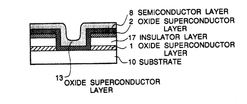
As shown in Figure lA, a substrate 10 having a subs~nti~lly planar
20 principal surface was prepared. This substrate 10 was formed of a
SrTiO3 (110) substrate or another insulator substrate such as a MgO (1003
substrate.
As shown in Figure lB, a c axis orientated YlBa2Cu307.~ oxide
superconductor layer 1, a SrTiO3 insulator layer 17 and a c-axis
25 orient~ted YlBa2Cu307 ~ oxide s~r~onductor layer 2 were deposited and
st7~cl~e~1 on the principal surface of tbe substrate 10 by for example an
o~f-axis sputtering, a reactive co-evaporation, ~n MBE (molecular beam
20793~7
epita~cy~, a CVD, etc. The c-axis orientated Y~Ba2Cu307.~ oxide
supelec~ ctQr layers 1 and 2 had a thickness of about 400 nanometers
and lc~pec~ ely constituted super~onducting current paths through which
superconducting current flew in parallel to the substrate 10. The
5 in~ tor layer 17 might be formed of MgO instead of Sr'riO3. The
condition of forming the c-axis orientated YlBa~Cu307.~ oxide
~u~rc~ ctor layers 1 and 2 by off-axis sput~ering was as follows:
Sputtering Gas Ar: 90%
2: 10%
Total pressure S x 10-2 Torr
Tcmper~ture of the subst~te ~00C
Then, as shown in Figure lC, a po~ion 30 of the stacked structure
in~lu~ p ~e c-axis orientated YIBa2Cu307.~ oxide superconductor layers
1 and 2 and the insulator layer 17 was etched by a reactive ion etctlin~
proc~ss using a chlor~c gas so that a surface of the substrate 10 was
exposcd.
A venical current path, such as a via hole, which connects ~e c-axis
o,;c~ltated oxide superconductor layers 1 and 2 will be forrned at the
portion 30.
Thereafter,as shown in Fig~lre lD, a Lal sBal.sCu307.y oxide
semiconductor layer 8 having a thickness of 100 nanometers was
llclJos;~ed on the c-axis orientated YIBa2Cu307.~ oxide superconduceor
layer 2 and the exposed portion of the substrate 10 by a sputtering
process. The condition of forming the Lal.sBal.sCu307 y oxide
semiconductor layer 8 by slJut~ g was as follo-lvs:
Spul~,iug Gas Ar: 50%
2: 50%
- 10 -
20793~7
Total pressure S x ~0-~ Torr
T~l~er~ re of ~e substrate 700~C
The oxide semiconductor layer 8 may be formed of
Lal.sCal.sMn3O~ z oxide semiconductor instead of Lal.sBal sCu3o7 y oxide
semicon11lctor. An oxide superconductor in contact with these oxide
semiconductors shows a long-range proximi~y effect so that the
s~ercollducting current flows through a relatively long distance in the
semiconductors.
Finally, as shown in Figure lE, an a-axis orientated Y~Ba2Cu3O7.
oxide su~lconductor layer 13 was formed on the Lal.sBal sCu3O7.y oxide
semicon~ ctor layer 8 by an MBE process so th~t the supercon~uctin~
c~ t path in accordance with the present invention was completed. An
MBE co~l~ition under which the a-axis orientated YlBa2Cu3O7.~0xide
s.~ c~ c-tor layer 13 was folmed was as follows:
Mol~c~ rbeam source Y: 1250C
Ba: 600C
Cu: 1040C
Pressure S x 10-5 Torr
Ten~ ature of the substrate 630C
The a-axis orientated YlBa2Cu307.~ oxide superconductor layer 13
was electrically connected to the c-axis orientated oxide superconductor
layers 1 and 2 through the ~al ~Bal sCu3O7 y oxide semiconductor layer 8,
since the superconducting current passed the Lan~B~ sCu3O7.y oxide
semiconductor layer 8 by ~he long-range proximity effect. Namely, two
horizontal superconducting current paths of the c-axis orientated
YlBa2Cu3O7~0xide superconductor layers 1 and 2 was electrically
- 11. -
2079357
connected through a vertical superconducting current path of the a-axis
o.i~t~l~d YlBa2Cu3O7 ~oxide superconductor layer 13.
The above mentioned superconducting path in accordance with the
present invention has a Lal.sBal sCu3O7-y oxide semiconductor layer
l~t~cw~ horizontal superconducting current paths of c-axis orientated
oxide su~c~eonductor layers and a vertical superconducting current path
of a a-a~is orientated oxide suye-c~nductor layer. Therefore, ~ere is no
grain boundary of the oxide superconductor at the interfaces between the
horizontal superconducting current paths and the vertica} su~crconducting
c~.ellt path. The superconducting current can pass ~he Lal.sBal~scu3o7 y
oxide sen iconductor layer by a long-range proximity effect so that there
is no Joseph~on junction nor electric resistance at the interfaces. By this,
d~e cu.lent capability and characteristics of the superconducting path can
be improved.
lS
Embodiment 2
Referring to Figures 2A to 2F, a process for manufacturing an
embodir~e.n~ of the superconducting device in accordance with the present
mvcntion will be described.
As s~own in Figure 2A, there was p~epared a substrate 10, sirnil~r
to ~e sul~ll~te 10 of the Embo~ .t 1.
As shown in Figure 2B, a c-axis orielltated YlBa2Cu3O7.~0xide
su~crconductor layer 2 havin~ a thickness of about 5 nanometers was
fo~ cd on a principal surface of the substrate 10 by for example an
off-a~cis sputtering. The off-axis sputtering was performed under the
same co~ditiotl as that of the Embo~ ent 1.
2~7g~57
Then, as shown in Figure 2C, a MgO insulator layer 17 having a
thicl~nes~ of 10 nanometers and an Au layer lS were deposited on the
c-axis orientated YlBa2Cu3O7.~0xide superconductor layer 2. The Au
layer lS, ~e insulator layer 17 and the c-axis orientated YlBa2Cu307.~
oxide su~rco~lductor layer 2 were processed by an Ar-ion etching so that
a gate ~lectrode ~, a gate ins~ tor 7 and a supercondllcting ch~n~el 20
we~e folmed on a center portion of the substrate 10, as shown in Figure
2D. In ~is connection, the gate inclllfltor 7 was side-etched in con~p~rison
wi~ ~e gate electrode S, so that the gate insulator 7 had a length shorter
~an that of the gate electrode 5.
The gate insulator 7 can be formed of SrTiO3 and the gate electrode
c~m be forrned of Ag.
Thereafter, as shown in Figure 2~, a Lal.sBal sCu307 y o~ide
scmiconductor layer 8 having almost the same thickness as the
~upcrconducting channel 20 was deposited on the the substrate 10 at the
bo~ sides of the superconducting channel by a sputtering process. The
sputtering was performed under the same condition as that of the
~m~li~ t 1 .
The oxide semiconductor layer 8 may be formed of
Lal.sCal sMn3O7 z oxide semiconductor instead of Lal.sBal sCu3o7-y oxide
semiconductQr. An oxide superconductor in contact with these oxide
semiconductors shows a long-range proximity effect so that the
~crcollducting current f~ows through a relatively long distance in the
~n~ic~ldll~t~rs .
Fina}ly, as shown in Figure 2F~ a superconducting source region 3
and a superconducting drain region 4 of an ~-axis orientated
YlBa2Cu3O780xide superconductor thin film were formed on the
- 13 -
2079357
Lal sBa~.sCu3O7 y oxide semiconductor layer 8 at both sides of the gate
in~ atc!r 7 and on the gate electrode 5, respectively. The MBE condition
under which the superconducting source region 3 and the superconducting
drain region 4 are formed is s~ne as the Embodiment 1.
A metal source electrode ~nd a metal drain eleetrode might be
f~ e~ on ~e superconducting source region 3 and the supercon~-~ctin~
drain region 4 respectively, if necess~ry~ With this, the super-FET in
accord~lc~ with the present invention was completed.
The above mentioned super-FET in accordance with the present
invention has a Lal sBal ~Cu307.y oxide semiconductor layer 8 ~etween
~e superconducting ch~nnel 20 and the superconducting source region 3
and let~ecn the superconducting channel 20 and the superconducting
drain region 4. Therefore, there is no grain boundary of the oxide
s.l~rc~l.d~lctor at the interfaces between the superconducting ch~nnel 20
and ~c supercondl~cting source region 3 and ~etween the supercot~ cting
~l~z..~ 0 and dle superconducting drain region 4. The superconducting
cullenl can pass the Lal sBal.sCu3O7 y oxide semiconductor layer 8 by a
long-range proximity effect so that there is no Josephson junction nor
clectric resistance at the interfaces. By this, the current capa~ility and
20 ch~acteristics of the super-FET can be improved.
In ~e aboYe mentioned embo~liments, the oxide supercondllctor thin
film can be formed of not only the Y-Ba-Cu-O compound oxide
su~erconductor material, but also a high-TC (high critical temperature)
o~ide superconductor material, particularly a high-TC copper-oxide type
25 c~ sund oxide superconductor material, for example a Bi-Sr-Ca-Cu-O
compound oxide supercon~lJctor~,naterial.
- 14-
2079357
The invention has thus been shown and described with reference to
~e speci~lc embodiments~ However, it should be noted that the present
invention is in no way limited to the details of the illustrated structures
but converts and modifications may be made within the scope of the
5 app~e~l cl~irns