Note: Descriptions are shown in the official language in which they were submitted.
2 2079418
FIELD OF THE INVENTION
This invention relates to an apparatus and
a method for manufacturing prototype printed circuit ;
boards. -~
BACKGROUND OF THE INVENTION
A printed circuit board is formed from a
thin board of electrically non-conducting material in -~-
which is formed a partly connected and partly
disconnected network or matrix of electrically
conducting elements. To make a particular circuit on
a printed circuit board, components must be placed on -
the board with electrical connections between them
being made by the matrix. However, many electrical ~`
circuits are quite complex and require much testing
and moving around of the circuit components. This
means that the circuit board on which the original
circuit is placed should allow the leads to be easily
removed from the board and re-inserted into the board,
while making good electrical connections when inserted
into the board. For this reason, a breadboard is often
used to prepare the initial circuit. The breadboard
has a particular matrix of electrically connecting
elements and this matrix is used to connect the ~ ;
components. Once the prototype circuit is made and
proven to ~e functional, it must be converted to a
prototype printed circuit board. This is accomplished -
largely as follows. -
1. The layout of the circuit is copied onto paper.
2. An experimenter's board of a suitable size is
obtained. This board will have its own matrix of
electrical connections that will not necessarily .~
match the breadboard matrix. ~- -
'-
2~7~
3. The circuit layout from the breadboard matrix is
converted to a matrix suitable for the type of
experimenter~s board being used.
4. All components are removed from the breadboard
and placed on the experimenter~s board according
to the layout developed in step 3.
5. All components and jumper wires are soldered in
place on the experimenter~s board, and traces
cut.
At this stage a hard wired prototype now
exists, and is ready to be tested. However due to the
complexity of this process there is considerable room
for errors to be made and it is typical that even an
experienced technician will expect to have to spend
substantial additional time retracing and debugging
the board.
SUMMARY OF THE INVENTION
With the system of the present invention,
this entire process is unnecessary. Using the system
of the present invention, the initial breadboard
prototype is turned into a hard wired prototype in one
simple step. This i6 accomplished by the printed
circuit board in effect creating the surface of the
connector matrix which, once the prototype is
functional, is removed from the connector matrix and
soldered to create the final prototype. This unique
process is believed to reduce the time required to
produce a prototype by approximately 90% and to ensure
that each prototype board will be fully functional
upon completion.
There is therefore provided in accordance
with one aspect of the invention, a circuit board
assembly system for manufacturing a prototype printed
2079~18
circuit board having a matrix formed in it, the
assembly system comprising:
a base board having a connection matrix that
matches the matrix of the printed circuit board; and
positioning means connectable to each of the
base board and the printed circuit board for locating
the printed circuit board in a fixed position relative
to the base board.
According to a further aspect of the
invention, there is provided a method of constructing
a prototype board using a base board having a
connection matrix, the prototype board having a
matching matrix that matches the connection matrix,
the method comprising the steps of:
locating the prototype board in a fixed
position relative to the base board with the matching
matrix aligned with the connection matrix;
inserting components having leads into the
prototype board with the leads extending into the base
board in electrical connection with the connection
matrix to form a circuit;
testing the circuit;
removing the base board from the fixed
position in relation to the prototype board; and
soldering the leads of the components into
the prototype board.
Further aspects of the invention will be
found in the detailed description of the invention and
in the claims that follow.
8RIEF DESClRIPTION OF THE DR~WINGS
There will now be described a preferred
embodiment of the invention, with reference to the
2079~18
drawings, by way of illustration, in which like
numerals denote like elements and in which:
Figure 1 is a perspective view, partly
broken away and exploded, of an apparatus according to
the invention with printed circuit board in place, the
printed circuit board including a matrix of
electrically conducting elements, some long and some
short;
Figure 2A is a cross-section through the
apparatus shown in Figure 1 parallel to the shorter
elements with a single component shown about to be
inserted in the apparatus;
Figure 2B is a cross-section through the
apparatus shown in Figure 1 perpendicular to the
shorter elements with several components inserted in
the apparatus; .
Figure 2C is a cross-section through the
apparatus shown in Figure 1 parallel to the shorter
elements with a single component shown about to be
20inserted in the apparatus, with springs inserted
instead of clips for retaining the leads of the
component;
Figure 3 is a perspective showing a printed
circuit board being inserted for testing in the
25apparatus shown in Figure 1 together with a cover;
Figure 4 is a perspective showing a printed
circuit board in place for testing in the apparatus
shown in Figure 1 together with a cover; !
Figure 5 is a perspective of the apparatus .
30of Figure 3 with the cover closed; :
Figure 6 is a perspective of the apparatus
shown in Figure 3, upside down, with the base board
lifted away from the printed circuit board and with
"
-` 2 0 7 9 ~
the ends of circuit component leads in position for
soldering; and
Figure 7 is a perspective showing the
apparatus of Figure 3 with the prototype printed
circuit board being removed from the apparatus.
DETAILED DES~RIPTION OF PREFERRED EMBODIMENTS
In this patent document and particularly as
used in the claims: "connection matrix" in relation to
a board means a matrix of partially connected and
partially separated electrically conducting elements
that permits numerous circuit designs to be formed on
the board, depending on the placement of electrical
components on the matrix; "matching matrix" in
. -
relation to a given connection matrix means a matrixof partially connected and partially separated
electrically conducting elements which has the same (a
matching) layout as the connection matrix;
"electrically conducting element~ means an electrical
conducting wire or strip or similar device whose
primary purpose is to conduct electricity; and
"components" includes resistors, capacitors,
inductors, diodes, switches, transistors, semi-
conductor chips, transformers and other small scale
electrical devices.
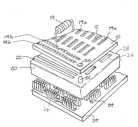
Referring to Figures 1, 2A and 2B, a printed
circuit board 10 of mostly conventional construction
includes a matrix 12 of electrically conducting
elements 14a and 14b. Individual electrical conducting
elements 14a and 14b are shown and for example may
simply form a short narrow strip 14a for receiving and
connecting several leads of components, or may form a
long narrow strip 14b for receiving several leads of
components and connecting them to a power source. The
2~79~18
elements 14a and 14b are for example formed from
narrow copper strips with openings 16 spaced along the
narrow strips. The openings 16 are preferably
countersunk as shown in Figure 2B at 17, that is,
tapered at the top, to allow for easy insertion of the
leads. The leads 18 of a component 19 may be inserted
into the openings 16 of the electrically conducting
elements 14a or 14b to extend through the printed
circuit board 10.
A base board 20 is formed from a non-
conducting slab-shaped base (for example made of a
suitable plastic) with a matrix 22 of electrically
conducting elements 24 fixed on or within the base for
receiving the leads 18 of components 19 such as the
resistor shown and other components (such as those
shown in Figure 2B) in the circuit being built.
Individual elements 24 preferably consist of a single
metal strip of clip type contacts as shown, for
example chrome plated steel, whose contacts are
separated no more than the width of the leads expected
to be inserted into them. Each clip should have
length and width slightly larger than the length and
width of a corresponding one of the linear openings or
slots 26 in the base board 20, each clip being
disposed within the base adjacent the corresponding
one of the openings 26. Referring to Fig. 2C, a
potential alternative to the clip is to use a spiral
metal spring 27. However, if springs are used one must
be careful to avoid arcing at the contacts, that might
occur if for example the contact with a lead was weak.
This might occur if there were leads inserted in
opposite ends of a spring, thus perhaps fixing the
spring in a pulled apart position and a further lead
was inserted between them. A further potential
2079~18
alternative to the clips or springs is to use
conductive elastomeric elements. Such elements would
be inserted (by injection moulding) into the base
board 20, filling the slots 26. Such injection
moulding could take place as a second step immediately
after the moulding of the base board 20. The
elastomeric elements would have holes to receive
leads. Such conductive elastomeric elements have the
desired advantage of contacting the lead on all sides
of the lead. Conductive elastomers are commonly
commercially available.
The function of an element 24 is to allow a
lead to be inserted into it while making an electrical
connection between the lead and the element, and to
prevent the lead from slipping out easily (for example
under its own weight) while allowing the lead to be
readily removable from the element by hand. Hence the
contact points of the element with the leads must have
sufficient compression to prevent the component from
falling out under its own weight.
The matrix 22 matches the matrix 12, so that
there is a one to one correspondence between the
electrically conducting elements 14a and 14b and the
electrically conducting elements 24. Each discrepancy
in the correspondence between the two matrices will
tend to reduce the efficiency of the apparatus and the
method of using it. Slots 26 in the upper surface 28
of the base board 20, one corresponding to each
element 24,; receive the leads 18 of components 19,
such as the resistor shown in Figure 2A. Barriers 30
are formed as part of the base board 20 to form
chambers for receiving and holding the elements 24.
The barriers 30 also form insulating barriers between
adjacent elements 24. Base board 10 is attached to a
2079~1~
base 34 by screws 39. An insulating layer 38 ~see
Figs. 2B and 2C) is preferably interposed between the
base 34 and the base board 10, so that the elements 24
do not make an electrical connection with the base 34.
Referring now also to Figure 3, the printed
circuit board 10 and the base board 20 are shown with
positioning means connectable to each of the base
board and the printed circuit board for locating the
printed circuit board in a fixed position relative to
the base board. The positioning means includes a
tracking frame 40 with grooves or channels 42 for
receiving the edges 44 of the printed circuit board
10. A connection edge 46 of the printed circuit board
10 mates with a matching connector 48 of the tracking
frame 40. A set of terminals 49 allow external
connection of leads to the connection edge 46 and
thence to the matrix printed circuit board 10.
Tracking frame 40 and the base 34 are hinged
to each other at a pivot 50. The end of the apparatus
near the pivot is referred to as the closed end of the
apparatus while the,opposite end is referred to as the
open end of the apparatus. A cover 52 is also hinged
at the pivot 50 to the tracking frame 40 and the base
34. All three parts, the tracking frame 40, the base
34 and the cover 52 are free to rotate with respect to
each other about an axis defined by the pivot 50,
preferably at least over about a 135 range.
As shown in Figure 3 and in Figure 1,
aligning posts 32 are formed in the two corners of the
base board at the open end. These posts 32 are
complementary to openings 36 in the printed circuit
board 10, and form means to facilitate the alignment
of the printed circuit board 10 and the base board 20
207941~
1 0
in relation to each other so that the matrices may be
aligned with each other, one on top of the other.
The cover s2 is formed with sides 54 and top
56, with a latch 58 at the end of the cover at the
open end of the apparatus. The latch 58 engages with
the printed circuit board lO when the printed circuit
board is fully inserted in the tracks 40 and the cover
is closed. A slot 60 in the base 34 is provided if
required so that the end of the latch 58 does not
contact the base board 20. A second latch (not shown)
may be provided to secure the cover to the base board
20 if desired. The cover 52 preferably includes a
padding and insulating material 62 such as foam rubber
attached, for example with adhesive, to the under side
of the cover. The tracking frame 40 and cover 52 are
preferably èach made of aluminum, but may be made of
other suitable material. The base 34 is preferably
made of steel.
Figure 4 shows an apparatus according to the
invention with a printed circuit board that has
numerous components 19, such as chip 68 inserted into
the printed circuit board 10, forming an electrical
circuit, with connections between the various
components 19 being made through the elements 24
forming the matching matrix of the base board 20.
There is also shown an oscilloscope 70 with leads 72
and lead bending device 74 for use in testing the
circuit on the printed circuit board 10. !
Figure 5 shows the apparatus according to
the invention in the closed position with cover 52
closed and secured with latch 58 fastened about
printed circuit board 10 to retain the cover 52 and
the printed circuit board together. The padding 62
rests gently against the components 19 to prevent them
-`: 2079~1~
11
from falling out of the elements 14a and 14b and 24
when the apparatus is inverted as shown in Figure 6.
Figure 6 shows the apparatus inverted, with
the base board 20 rotated up and away from the
underside of the printed circuit board 10. The leads
18 of the components 19 have been freed from the
elements 24 and protrude from the underside of the
printed circuit board 10. In this condition, no good
connection is made between the leads 18, until
soldered to the printed circuit board 10 to make an
electrical connection with the matrix of the printed
circuit board, using the soldering iron 80. Cutters 82
are used to sever the ends of the leads 18 that
protrude from the solder.
The method of operation of the apparatus
will now be described.
Rèferring to Figure 3, the cover 52 pivots
on the pivot 50 to allow access for the printed
circuit board 10 into the apparatus. The printed
circuit board 10 is inserted into the apparatus by
sliding it along the side tracking frame 40 until it
identifies with the edge connector 46 at the base or
closed end of the printed circuit board tracking frame
40. The two lower sections of the apparatus (the
printed circuit board tracking frame 40, and the base
board 20 with connection matrix) are snapped together
with the identifying posts 32 and openings 36
automatically aligning the matrix 12 of the printed
circuit board 10 with the connection matrix 22 of the
base board 20 thus preparing the system for component
insertion.
Referring to Figure 4, leads 18 of
components 19 are inserted through the printed circuit
board 10 into the connection matrix 22 thus providing
207941~
12
an electrical connection between the components 19.
This connection, provided by the elements 24 embedded
in the plastic base board 20, is identical to the
final connection provided by the copper tracks 14 of
the printed circuit board 10. Through the built-in
connection interface points or terminals 49 at the
closed end of the apparatus, connections are made to
the matrix 22 and printed circuit board 10 thus
allowing for testing and modification of the circuit
for example with the oscilloscope shown.
~ eferring to Figure 5, upon completion of
the circuit, or to facilitate transport of an
uncompleted circuit, the cover 52 of the apparatus
with the padding 62 (the compression stage) is pivoted
down until it latches into place on the printed
circuit board 10 (using the latch 58) and, if desired,
the base board 20 (using a further latch, not shown),
thus securing all the components from being dislodged.
,
Referring to Figure 6, in order to allow
access to the solder side (under side) of the printed
circuit board 10, the entire apparatus is first
inverted, and then base board 20 is rotated away from
the printed circuit board 10, tracks 40 and cover 52,
with the connection matrix 22 disengaging from the
leads 18 of the components 19 on the printed circuit
board 10. This exposes the component leads 18 of the
circuit, and the solder side of the printed circuit
board 10, all held together by the latch 58.
While the components 19 are securely held in
place in the printed circuit board 10 by the pressure
exerted on the components 19 by the compression stage
(cover 52 and padding 62), the component leads 18 are
soldered into place on the printed circuit board 10.
When all the leads are soldered into place, and the
2~9418
13
additional length is trimmed from all the leads, the
board is complete.
Rèferring to Figure 7, the latch 58 is
released from the printed circuit board 10, thus
allowing the printed circuit board 10 to be swung
clear of both the compression stage (cover 52 and
padding 62) and the base board 20, thus allowing the
completed and tested printed circuit board 10 to be
removed from the apparatus. The completed printed -
circuit board 10 is ready for insertion into whatever
application it was designed for.
Alternative Embodiments
A person skilled in the art could make
immaterial modifications to the invention described
and claimed in this patent without departing from the
essence of the invention.
' '" ~