Note: Descriptions are shown in the official language in which they were submitted.
7 ~ 2
- 1 -
MULTIPLE VIRTUAL FIFO ARR4NGEMI :NT
Technical Field
The invention relates to buffering data packets received at a packet
switch and more particularly relates to providing at a paclcet switch a virtual FIFO
5 for each source of data packets.
Back~round of the ~vention
A data buffer, such as a FIFO memory buffer, is typically used to
interface a source of data with a port circuit of a packet switch. In certain instances,
a port circuit may serve a plurality of sources of data associated with different grades
10 of service, including, for example, latency, reliability, bandwidth, etc. In such a
situation, a data buffer is provided for each data source, with the data buffer si~ed to
handle the transfer of a large file, taking into account the throughput of the
associated packet switch. It can be appreciated, therefore, that if a po~t circuit is
serving a large number of data sources, e.g., 512, then the port would have to be
15 equipped with an equal number of data buffers. It can also be appreciated that the
administration of a large number of data buffers would indeed be a complex task,thereby making the associated port circuit complex. Moreover, if each buffer is
formed from a large number of memory locations, then the cost of equipping a port
circuit with a large number of buffers would indeed be expensive.
20 Summary oî the ~vention
An advancement in the art of packet switchin~ is achieved by providing
for each of a plurality of sources of data served by a port circuit a virtual FIFO
having a storage capacity that dynamically increases and decreases as required by the
associated source.
In an illustra~ive embodiment of the invention, a plurality of virtual
FIFOs is implemented by partitioning memory internal to a port circuit into a
plurality of data buffers, in which ones of the data buffers are associated withrespective ones of the data sources. The remaining data buffers are then used toform a pool of data buffers such that, if the capacity of a data buffer associated with
30 a source is exhausted, then that data buffer is linked to a data buf~er obtained fFom
the pool to increase the capaci~ of the associated data buffer. When a linked data
buffer is emptied, then it is returned to the pool to decrease the cap~ci~y of the
associate~l data bu~fer.
2 ~
- 2 -
Brief Description of the Dra.win~
In the drawing:
FIG. 1 is a broad block diagram of a telecommunications switching
system in which the principles of the invention may be practiced;
FIG. 2 is a n illustrative exarnple of the format of a data packet;
FIG. 3 illustrates the ma~mer in which memory internal to particular
ones of the port circuits of FIG. 1 is partitioned in accord with the principles of
invention;
FIG. 4 illustrates the layout of a channel record of FIG. 3;
FIG. S is an illustrative broad block diagram of a port circuit of FIG. 1;
and
FIG. 6 is an illustrative example of the way in which a virtual FIFO
expands a. d cont.~cts in al~cord with the principles of tne invention.
Detailed Description
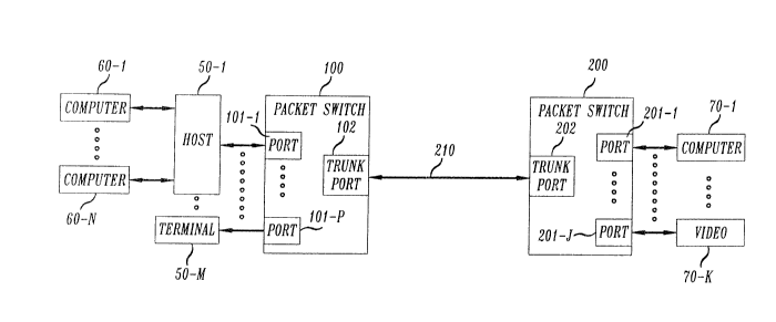
FIG. 1 is a broad block diagram of a switching system comprising a
plurality of telecornmunications switches te.g., packçt switches), two of which,packet switches 100 and 200, are shown in the FIG. As is well known, such packetswitches may be arranged to exchange witn one another data packets originated byrespective sources of da~a, such as computers 60-1 throu~h 60-N. In certain
20 instances, one or nore packet switches may serve as an intermediate switch between
origination and destination packet switches.
Typically, a packet switch includes, inter alia, a controller, memory and
clock circuit (not shown), which control the overall operation of the associatedpacket switch. A packet switch also includes a plurality of port circuits for
25 interfacing the associated switch with resyectively (a3 sources of data packets, and/or
~b) communications paths extending to other packet switches. For example, port
circuits 101-1 through 101-P interface switch 100 with computers 60 1 through 6~N
and teTminal 50-M, respectively, whereas trunk port cir~uit 102 interfaces switch 1~)
with communications path 210 e~ctending to switch 200. Each such port circuit is30 typically identified by a respective port addless and is associated with one s~r more
chann I addresses (numbers). A port circuit uses such channel addresses to
res~ectively identify the data circuits that the port circuit serves. Switch 200 having
port circuits 201 through 201-J and trunk port 202, is similarly arranged. That is,
port circuits 201-1 through 201-J present an interface to sources 70-1 through 70-K
35 and tnmk port 202 presents an interface to communications path 210.
7J ~
The source computers may be any one of a number of different types of
computers. They may be, for example, personal computçrs, so-called workstations
or sources of images (video ~errninal). In addition, a plurality of computers may
connect to a packet switch port circuit via a common interface, e.g., host
S computer 50-1. Accordingly, in this embodiment, computers 60-1 thr~lgh 60-N
supply data packets that they generate to host computer 50-1. Most computer 50-1,
in turn, supplies packets that it receives to its associated port circuit 101-1 for
storage in respective sequential locations of a port circuit 101-1 m~mory buffer.
Typically, a port circuit memory buffer presents an interface to a
10 computer (or cornmunications path) and may be, for example, a s~called First-In,
First-Out (FlFO) memory. Data packets generated by a computer, or a number of
computers, are thus stored in respective sequential locations of an associated port
circuit FIFO. The associated port c~rcuit, in turn, unloads the data packets in the
order that they were stored in its associated FIFO and forwards them to their
15 intended destinations.
It can be appreciated that under certain conditions, such as, for exarnple,
when a majority of the computers 60 1 through 60-N are active, port circuit 101-1
could receive via host 50-1 a steady stream of data packets. Moreover, one or more
of the computers 6(}1 through 60-N could be engaged in transfening very large files
20 to other computers, either associated with switch 100 or another switch, such as
switch 200. In such a situation, the buffer interface between host 50-1 and portcircuit 101-1 could 'oe overloaded, thereby possibly causing one or more data packets
to be lost.
As mentioned abc-ve, one prior art arrangemenc deals ~,vith this problem
25 by providing a port cir~uit input buffer, e.g., a FIFO, for each computer 60-1 through
60 N. In addition, each such input buffer is typically sized to handle the ~ansfer of a
very large file taking into account the capacity of the associated packet switch. It can
be appreciated that if N is a large number, e.g., 512, then a cor~esponding number of
port circuit input buffers would have to be provided. Moreover, if each such buffer
30 is formed from a large number of memory locations, then the cost of providing the
buffers would indeed be expensive.
We deal wi~h this problem by initially assigning to each computer 61)-1
through 60-N a small buffM that is sized to accommodate an average stream of data
packets. Moreover, in accord with an aspect of the invention, the capacity of such a
35 buf~er is allowed to dynamically expand to accommodate an increase in the stream
of data packets generated by the associa~ed source computer.
r~
Before proceeding with a discussion of our invention, we believe it
would he best at this point to discuss an illustrative fonnat of a data packet that a
port circuit, e.g, circuit l01-1, may receive at its input for storage in an associated
data buffer. An illustrative fornnat of a data packet is shown in FIG. 2 and may5 include a data information field 20 and header 21. As is well known, ths data that a
computer, or terminal, e.g., computer 60^1, sends to another compslter is inserted in
inforrnation field 20. As is also well known, a packet header typically contains, inter
alia, a conventional error check field 21-1, OA field 21-2 identifying the add~ess of
the originator of the packet and DA field 21-3 identifying the intended recipient
10 (destination) of the packet. In an illustrative embodiment of the invention, the
address of the originator that is inserted in OA field 21-2 may inslude (a) a channel
number associated with the sender of the data, (b) the address of the associatedpacket switch port circuit and (c) the address of the associated packet switch. The
contents of DA field 21-3 may be similarly arranged.
Turning now to FTG. 3, there is shown a block of memory 3C)0 which is
internal to a port circuit, e.g., port circuit 101-1 or trunk pon 102. It is seen from the
FIG. that memory 300 is partitioned into a number of sections 301 through 304.
Section 301 comprises a number of data buffers -- illustratively 1792 buffers --designated 301-1 through 301-P. Each such data buffer is forrned from a
20 predetermined number of bytes of memory 300, for example, 128 bytes with eachbyte having eight bits. When power is initially applied to a port circuit and the latter
is therefore "booted up", a port controller (not shown) initializes the data buffers. In
doing so, the port controller assigns to each of its associated channel addTesses a
respecti~e data buffer and marks the remaining data buffers as being "free"
25 (unassigned). For example, if the port circuit is associated with 512 channels, then
512 channels are initially assigned respective data buffers (c.g., buffer 1 through M).
The remaining 12B0 data buffers (e.g., buffers M+l through P) are marked free. The
f~ee data buffers are used, in accord with an aspect of the invention, to increase
dynamically the capacity of an assigned data buffer as needed.
For example, assume that a computer, e.g., computer 6()-1, is
~ransmitting data packets at a rate faster than the rate at which por~ circuit 1()1-1 can
unload data packets from the data buffer assigned to the channel number associated
with computer 60 1. Also assume that, as shown in FI(~. 6, the assigned data buffer
is data buffer 6(31. As a result, data buffer 601 would become full at time t0. To
35 increase the data bu~ér capacity presently required by computer 60-1, then, in
accord with an aspect of the invention, port circuit 101-1 increases the capacity of
~ ~3 7 ~ 5 ~ . ?
- 5 -
the assigned data buffer by linking a free data buffer 602 to the former data buffer at
time ta. Port circuit 101-1 then stores data paclcets newly received from
computer 60-1 in the linked data buffer 602. If buffer 602 becomes full, then port
circuit 101-1 links another free data buffer 603 to the priorly linked da~ buffer 602
S at time tb. In the general case, port circuit 101-1 continues to link free data buffers
to one another as long as computer 60-1 requires the additional data buffer capacity.
Assume in the instant example that ~hree buffers are adequate. When
port circui~ port 101-1 unloads from the initially assigned data buffer 601 the last of
the data stored therein, then port circuit 101-1 marks buffer 601 as being free. Port
10 circuit 101-1 at time tc then assigns buffer 602 to the associated channel number.
Sirnilarly, when port circuit unloads from buffer 602 the last of the data stored
therein, then port circuit 101-1 marks buffer ~2 as being free, as shown at time tc.
Port circuit 101-1 then assigns buf~er 603 to the associated channel number.
However, in accord with an aspect of the invention, the last of such linked data15 buffers, namely buffer 603, is not marked free, but, as shown at time td, remains
assigned to the associated channel even though buffer 603 may be empty, as will be
discussed below. Thus, in accord with an aspect of the invention, each port circuit
channel number associated with a computer that is served by port circuit 101-1 is
assigned what we call a vir~ual FIPO whose capacity may increase or decrease as
20 required.
Port circuit 101-1 tracks such linking and unlinking of data buffers
forming a virtual FIFO by maintaining a channel record that is assigned to the
associated channel number, as shown in FIG. 3. Specifically, channel records ar~stored in section 302 of memory 300, and may be indexed using a respective channel
25 number. For exarnple, channel record 1 is associated with channel 1, channel
record 2 is associated with channel 2, and so on. Thus, a port circuit uses a channel
number as a memory section 302 index to access the associated channel record.
Briefly referring to FIG. 4, it is seen that a channel record includes a
plurality of fields for the storage of respective pointers and other information.
30 Included in such pointers is Head Pointer (HP) 302-11, which points to the last data
entry of the last data buffer currently assigned ~o the respective channel number, and
Tail Pointer (TP) 302-21, which points to the first data entry of the first data buffer in
a chain of data buffers, if any. The other information is inserted in field 302-22.
Re~urning to FlG. 3, the linking between data buffers forming a chain of
35 data buffers, if any, is tracked by buffer link records forming section 303 of
mems)ry 30û. That is, a section 303 link record associated with a data buffer in a
~`l,7 5J ~
- 6 -
chain of data buffers identifies the address of the next succeeding data buffer in the
chain. In an illustrative embodiment of the invention, a memory section 303 linkrecord is accessed using what we call a logical index. In an implçmentation of the
invention, a logical index is generated by shifting the contents of a particular scratch
S register to the right by five bit locations and then inserting a zero in each of the two
low-order bit locations. A particular section 303 link record is then accessed using
the starting address of memory section 303 as indexed by a logical index.
Section 304 of memory 300 serves as a conventional circulating register
for the storage of addres~ses identifying available data buffers, i.e., "free" data
10 buffers. During the aforementioned initialization, the associated port circuit, e.g.,
port 101-1, stores the addresses of respective "free" data buffers in sequentiallocations of memory section 304. In an illustrative embodiment of the invention and
as will be explained below, a pointer (Read Free Pointer) is used to identify the
section 304 location contaimng the address of the next free data buffer. As will also
15 be explained below, the address of a linked data buffer that no longer contains data,
i.e., is made available for use (free), is stored in a section 304 locadon identified by
another pointer (Write Free Pointer).
Turning now to FIG. 5, interface circuit 705 is arranged to receive from
a source 600, such as, for example, host computer 50-1, a stream of data packets.
20 The originators of such data packets may be the devices that source 600 serves, such
as computers 60 1 through 60 N. Input interface circuit 705, inter alia, stores data
words (bytes) as they are received in sequential memoTy locations of conventional
memory FIFO 710 via bus 706, in which a plurality of such data bytes forrn a
respective data packet.
Data controller 720 serves as one of the means for ~ransfeITing data
bytes that have been stored in FIFO 710 to a respective data buffer. In particular,
controller 720 unloads a data packet four bytes ~words) at a time in the order that the
bytes were stored in FIFO 710. Controller 720 then stores the unloaded data bytes in
register 725 via bus 711. Controller 720 then checks via bus 711 the contents of30 register 725 to deterrnine if such contents represents a channel number, thereby
indicating the beginning of a packet. If that is not the case, then controller 720
notifies sequencer 715 that a new set of data bytes of an incoming data packet has
been stored in register 725.
Assume that a newly arrived channel number has been stored in
35 register 725. In that event then, sequencer 715 causes particular informationcontained in register 732 and asslxiated with a preceding data packet processed by
~ U q~ _ ~J ~
sequencçr 715 to be stored in the respective ch~mnel record, as will be explained
below. Sequencer 715 then directs register 725 to output the new channel number to
data bus 315 so that the number may be latcned in channel registçr 733.
Sequencer 715 then unloads from memory section 302 the channel record associated5 with the new channel address contained in channel register 733. In doing so,
sequencer 715 places on address bus 320 the star~ing address of memory section 302
as indexed by the contents of rçgister 733. Sequencer 715 then prompts RJW
(Read/Write) cont~ol circuit 735 to assert a read signal on lead 310. Memory 300 in
response thereto and in a conventional manner reads and then outputs to data bus 315
10 the contents of the addressed section 302 location. Sequencer 715, in turn, causes
the information appearing on data bus 315 and, in particular, the value relating to the
aforementioned data buffer Head Pointer (HP) to be stored in register 732.
Sequencer 715 then waits for receipt via path 721 of a controller 720 notification
indicating that the next set of data by,es has been stored in register 725.
In response to such notification, sequencer 715 causes the contents of
registers 725 and 732 to be placed on data and address busses 315 and 320,
respectively. Sequencer 715 then prompts RJW control 735 to assert on lead 310 awrite signal, thereby causing memory 300 to store in the addressed data buffer the
infonnation appearing on bus 315. Sequencer 71S then increments the contents of
20 HP register 732 by a predetennined value -- illustratively a value of four -- so that
such contents point to the next location of the ~ta buffer currently associated with
the channel num'oer contained in register 733. Sequencer 715 then waits for receipt
of the next such notification.
Sirnilarly, controller 720 unloads the next four data bytes from
25 FIFO 710 and stores ~hem in register 725. Assume that the data bytes that are now
stored in regis~er 725 are part of the data packet associated with the channel number
stored in register 733. In that event, then, eontroller 720 notifies sequencer 715 of
that fact, as mentioned above. Sequencer 715, in the manner described abo~e, stores
the data bytes in the data buffer location identified by ~he current contents of HP
30 register 732. Sequencer 715, as mentioned above, then increments register 732. The
associated port circuit continues processing data bytes successively stored in
register 725 until that register contains a channel num1xr that is different from the
channel number currently contained in register 733, thereby possibly indicating the
start of a data packet associaled with another channel number. In that event,
35 se~uencer 715 causes the head pointer contained in register 732 to be stored in the
channel record associated with the channel number currently contained in
- 8 -
register 733. Sequencer 715 accomplishes that Itask by causing the contents of
register 733 as well as the memory section 302 starting address to be placed on
address bus 320. In addidon, sequencer715 causes the contents of register732 to
placed on data bus 315~ Sequencer 715 then prompts R/W circuit 735 to assert a
S write signal on lead 310. Memory 300, in response thereto, stores the data on
bus 315 in the addressed channel record.
As mentioned above, a data buffer comprises illustratively 128 data
bytes, such that each such data buffer starts at a 128 by~e boundary of section 301
memory. Since seven binary bits may be used to track a maximum count of 127,
10 then the lowest seven bits of the contents of HP register 732 may be used to indicate
when a data buffer is full. Accordingly, if register 732 contains a count of 124 and is
incremented by a value of four, then the low-order seven bits of the contents ofregister 732 would have a value of zero, thereby indicating that the associated data
buffer is full. To determine when a data buffer is full, sequencer 715 thus "tests" the
15 contents of register 732 each time it increments that register. If sequencer 715 finds
that the low-order seven bits of register 732 equals zero, then sequencer 715 links a
free buffer to the current "full" data buffer associated with the channel numbercontained in register 733.
To track the location of the next "free" data buffer, a port circuit, during
20 initialization, stores the address of the first section 304 memory location in RFP
(Read Free Pointer) register 731 and stores the address of the last section 304
memory location in WFP (Write Free Pointer) register 741. In addition, the
associated port circuit stores in the first location of memory section 304 the address
of the first free data buffer. The port circuit also stores the addresses of the25 rernaining ~ee data buffers in respective succeeding section 3W locations.
Accordingly, sequencer 715 may link a free data buffer to a full data
buffer assigned to the channel number contained in register 733 to create a chain of
data buffers, i.e., a virtual FIFO. To do so, sequencer 715 obtains a free buffer and
then links that buffer to a full data buffer. In particular, sequencer 715 causes the
30 address of a memory location in memory secdon 3W as indexed by the contents of
of RFP register 731 to be placed on address bus 320. Sequencer 715 then prompts
R~W control 735 to assert a read signal on lead 310. Memory 300 responsive thereto
reads and places on data bus 315 the contents of the addressed memory 304 location.
Sequencer 715, in turn, causes the information appearing on data bus 315 to be
35 stored in scratch register 736. Sequencer 715 then links the newly acquired data
buffer to the full buffer by (a) causing the contents of scratch register 736 to be
J ~.
- 9 -
placed on data bus 315, and (b) causing the ad~ess of memory section 304 modified
by a logical index derived ~rom the contents of lHP register 732 to be placed onaddress bus 320. Sequencer 715 then prompts RIW control cir~uit to assert a wntesignal on lead 301. Memory 300 in ~esponse thereto stores the address of the newly
S acquired buffer in the section 303 link associated with the full data buffer.
Sequencer 715 then causes the data buffer address that had been placed on data
bus315 to be stored in HP register 732. In addition, sequencer 715 increments the
contents of RFP register 731by a value of one, so that such contents points to the
memory section 304 location containing the address of the next free data buffer. (It
10 is noted that register 731is alTanged as a modulo k counter such that, when the
contents of register 731 reaches a value of k and the register is incremented7 then
such contents cycles automatically to point to the first location of memo~y
section 304.)
The unloading of data words from memory 300 data buffers for delivery
15 to an intended destination is handled by read sequencer 745 responsive to receiving a
respective request message from output interface 750. The originator of such a
request message may be another circuit, which may be contained in the associatedpacket switch and which comrnunicates with interface 750 via path 752.
Alternatively, an originator of such a request ("request originator") may be external
20 to the associated packet switch. Destination 800 represents the various intended
recipients of data packets that have been stored in memory 300. The dashed portion
ofpath752 repTesents a path through the associated packet switch, e.g., switch 11)0,
and communications paths that may be traversed to reach such recipients, in which
such communications paths may be routed through one or more other packet
25 switches.
In particular, data packets associated with a particular channel number
may be unloaded from memory 300 by first supplying to output interface 750 via
bus 752 a request message identifying the particular channel nurnber. Ou~tput
interface 750 responsive to receipt of the message notifies read sequencer 745 via
30 bus 751 and outputs to data bus 302 the channel number contained in the request
message. Read sequencer 745 responsive to such notification ~a) causes the channel
number appealing on bus 302 to be stored in channel register 742, and ~b) obtains
~rom memory 300 the record associated with that channel number. That is, read
sequencer 745 (a) places on address bus 320 the start address of memory section 302
35 indexed by the channel number stored in register 742 and (b) causes R/W circuit to
assert a read signal on lead 301. Similarly, memory 300 in response thereto outputs
2~,....,,,,..,~
- 10-
to data bus 315 a copy of the inforrnation stored at the addressed channel lecord
location. Sequencer 745, in turn, causes the information contained in the Tail
Pointer (TP) field of the channel record appearing on data bus 302 to be stored in TP
register 743. Sequencer 745 then waits for a request to read the data stored in the
5 data buffer location identified by the contents of register 743.
In an illustrative embodiment of the invention, read sequencer 745
unloads from memory 300 one data buffer location for each request for data that it
receives via output interface 750. Accordingly, to obtain a stored data packet
associated with the channel number stored in register 742> the aforementioned
10 originator supplies a series of data requests to output interface 750. Outputinterface 750, in ~n, supplies each such request as it is received to sequencer 745
via bus 751. Alternatively, the request originator may obtain via interface 750 a
copy of the channel record. In this way, the request originator may determine the
number of requests that need to be supplied to sequencer 745 to obtain all, or a part
15 of such data.
Specifically, responsive to receipt of a request for data associated with
the channel number that is stored in register 742, read sequencer 745 causes thecontents of TP register 743 to be placed on address bus 320. In addition, read
sequencer 745 prompts R/W control circuit 735 to assert a read signal on lead 301.
20 Sirnilarly, memory 300 in response thereto reads and places on data bus 315 for
delivery to in~erface 750 the contents of the addressed data buffer location. Output
interface 750, in turn, outputs the data appearing on bus 315 to bus 752.
Following the foregoing, read sequencer 745 increments by a
predeterrnined value -- illustratively four -- the contents of TP register 743 so that
25 such contents point to the next location of the data buffer that is to be read.
Accordingly, sequencer 745 operates in the foregoing fashion responsive to receipt
of a subsequent data request or channel change request. In response to a channelchange request, sequencer 745 (a) stores the contents of register 743 in the TP field
of the section 302 record associated with the channel number contained in
30 register 742, (b) directs output interface 750 to ou~put the new channel number to
data bus 315, and (c) then causes the con~ellts of data bus 315 to be latched into
register 742. Read sequencer 745 ~hen obtains in the described manner the
section 302 record associated with the newly received channel nurnber and then
waits for receipt of a data request.
Like store sequencer 715, read sequencer 745 checks the value of the
contents of register 743 each time such contents is incremented. If sequencer 745
finds that the low-order bits -- illustratively bits 0 through 6 -- of such contents equal
zero, then sequencer 745 concludes that the data buffer that it had just addressed is
5 empty. In that instance, then, read sequencer 745 unlinks the data buffer if it
happens to be one of a chain associated with the channel number stored in
register 742, and then adds the unlinked buffer to the section 304 list of free data
buffers.
In particular, during initialization, the associated port circuit stores in
10 WFP register 741 the address of the next section 304 location that is to be used for
entering the address of the next data buffer that is completely unloaded by
sequencer 745. Thereafter, to add the address of an emptied data buffer ~o the free
list, or pool, sequencer 745 causes the ontents of registers 743 and 741 to ~e placed
on data and address busses 315 and 320, respectively. Sequencer 745 then prompts15 R/W control circuit to assert a write signal on lead 301. Memory 300, in response
thereto, stores the information contained on data bus 315 in the addressed locaeion.
In addition, sequencer 745 causes the inforrnation contained on data bus 315 to be
stored in scratch register 744. Following the foregoing, sequencer 740 increments
the contents of }egister 741 so that it points to the next location in memory
20 section 304 that is to be used for entering the address of a free data buffer.
To unlink the free data buffer from the chain, sequencer 745, as
discussed above, generates a logical index as a function of the contents of scratch
register 744 (address of unlinked buffer). Sequencer 745 then causes the address of
memory section 303 as indexed by the logical index to be placed on address bus 320.
Sequencer 745 then prompts RlW control circuit 735 to assert a read signal on
lead 310. Memo~y 300, in response thereto, outputs the contents of the buffer link
associated with the unlinked buffer to data bus 315, in which such contents is the
address of the next linked buffer of the chain. Sequencer 745 then causes the
information appearing on data bus 315 to be stored in TP register 743.
If the ernptied data bu~fer is not one of a chain of data buffers, then the
emptied data buffer remains asss~ciated with the channel number contained in
register 742.
In an illustrative embodiment of the invention, circuit 10 may also
include a Free Buffer S~atus ~FBS) circuit 755, which operatçs to ~rack the contents
of regis~ers 731 and 741. That is, FBS circuit 755 is arrangçd to notify
sequencer 715 whenever a free data buffer is not available. In particular, FBS
circuit 755 cornpares the contents of register 731 with the contents of register 741 to
track the instance in which all of the data buffers are 'oeing used. That is, ifregisters 731 and 741 contain the same value, then both registers are pointing to the
same rnemory section 3(34 location, thereby indicating that a free buffer is not5 available. If such a condition occurs, then FBS circuit 755 noeifies sequencçr 715 of
ehat fact via lead 756. Sequencer 715 in response thereto stops storing data bytes in
memory 300.
The foregoing is merely illustrative of the principles of the invention.
Those skilled in the art will be able to devise numerous arrangements, whish,
10 although not explicitly shown or described herein, nevertheless embody those
principles that are within the spirit and scope of the invention.