Note: Descriptions are shown in the official language in which they were submitted.
20B00~7
INFORMATION RECORDING/REPRODUCING APPARATUS FOR OPTICAL
INFORMATION RECORDING MEDIUM
BACKGROUND OF THE INVENTION
(Field of the Invention)
The present invention relates to an information
recording and reproducing apparatus for an optical
information recording and reproducing apparatus for an
optical information recording medium wherein information
is recorded by forming a pit upon application of a light
beam to the recording medium while aligning an optical
head to a track position, and information is read from a
pit by using the light beam.
(Description of the Related Art)
For an optical head, means is provided for
generating a tracking error signal whose polarity changes
between a positive polarity and negative polarity in
response to a track traverse by the optical head. A
track traverse detecting signal is generated by comparing
the tracking error signal with a reference signal.
A conventional information recording and reproducing
apparatus uses a fixed reference signal so that a
tracking error signal of a low level is not detected in
some case. Furthermore, when noises having substantially
a large level are generated in the circuit, these noises
may be detected as a track traverse, thereby forming an
incorrect track traverse detecting signal. Further, if
the optical system is adjusted improperly, a shoulder is
generated on a tracking error signal, thereby forming an
incorrect track traverse detecting signal. Still
further, an incorrect track traverse detecting signal may
be generated by a distortion of the tracking error signal
caused by dusts or scratches on the surface of an optical
image recording medium.
SUMMARY OF THE INVENTION
The present invention has been made under the above-
described circumstances.
-
2 ~ 20800~7
It is a first object of the present invention to
provide a motion controller for an optical head capable
of moving the optical head to a target position in a
short time while eliminating an error to be caused by
mechanical elements and without reading a present address
during the motion of the optical head from a far jump to
a near jump.
It is a second object of the present invention to
provide a jump controller allowing an optical head to
perform a near jump to a nearby track speedily.
It is a third object of the present invention to
provide a circuit for generating a track traverse
detecting signal capable of correctly detecting a track
traverse even if some errors are present on a tracking
error signal.
In order to achieve the above-described first
object, the present invention provides an information
recording and reproducing apparatus for an optical
information recording medium for recording and
reproducing information to and from the optical
information recording medium by scanning each track of
the medium with a light beam from an optical head, the
optical beam being moved from a first position to a
second position on the medium through a combination of a
far jump driving the optical head and a near jump driving
an objective lens assembled with the optical head,
comprising:
position reading means for scanning the medium to
read present address information;
position storage means for storing the present
address information;
traverse signal generating means for generating a
track traverse detecting signal by detecting that the
optical beam traverses the track on the medium;
motion amount detecting means being reset at the
start of the operation of the information recording and
reproducing apparatus, for receiving an output of the
208D057
traverse signal generating means and detecting a motion
amount of the optical head over the medium;
switching means for selecting an output of the
position storage means when an output of the motion
5 detecting means is zero, and selecting an output of the
motion amount detecting means when an output of the
motion detecting means is not zero;
target position receiving means responsive to a next
information recording and reproducing command for the
10 medium for receiving a target position;
direction designating means for determining a motion
direction by comparing the target position received by
the target position receiving means with one of the
present position stored in the position storage means and
the motion amount detected by the motion amount detecting
means;
motion distance calculating means for calculating a
motion distance by comparing the target position received
by the target position receiving means with the present
position stored in the position storing means, and
calculating the motion distance after the motion start by
comparing the target position with the motion amount;
on/off-controlling means for a tracking control for
performing a near jump scan when the motion distance
calculated by the motion distance calculating means is
smaller than a predetermined value, and performing a far
jump scan when the motion distance is larger than the
predetermined value;
motion speed controlling means responsive to a
selection of the far jump by the on/off controlling
means, for controlling to move the optical head in the
motion direction designated by the direction designating
means, by half the motion distance calculated by the
motion distance calculating means in an acceleration
mode, and by the remaining half of the motion distance in
a deceleration mode; and
4 20800~7
driving means for moving the optical head in
accordance with outputs from the direction designating
means and the motion speed controlling means.
The position reading means scans an optical
information recording medium to obtain present address
information. This address information is stored in the
position storage means, and supplied via the switching
means to the motion direction designating means and
motion distance calculating means. The address
information is compared with the target position from the
target position receiving means to obtain a motion
direction and motion distance.
When a light beam from an optical head traverses a
track, the motion amount detecting means detects the
motion amount of the optical head in accordance with a
signal generated by the traverse signal generating means.
This motion amount is supplied via the switching means to
the motion direction designating means and motion
distance calculating means.
The switching means selects an output of the
position storage means when an output of the motion
amount detecting means is zero, and an output of the
motion amount detecting means when the output is not
zero. The selected output is supplied to the motion
direction designating means and motion distance
calculating means.
An output of the motion direction designating means
is supplied to the driving means. An output of the
motion distance calculating means is supplied to the
motion speed controlling means whose output is supplied
to the driving means. If the motion distance is larger
than a predetermined value, a far jump is performed, and
if smaller, a near jump is performed. In the case of the
far jump, the on/off controlling means turns off the
tracking control. The driving means drives the optical
head in the direction designated by the motion direction
designating means by half the motion distance calculated
20800~7
by the motion distance calculating means in an
acceleration mode, and by the remaining half of the
motion distance in a deceleration mode. In the case of
the near jump, the motion speed controlling means causes
the driving means to perform the position control for the
tracking control. When the optical head comes near the
target position by the far jump, the control
automatically changes to the near jump to perform the
final tracking control.
According to the present invention, the motion
direction and motion distance are obtained, and if the
motion distance is larger than the predetermined value,
the optical head is moved by half the motion distance in
an acceleration mode, and by the remaining half of the
motion distance in a deceleration mode. Accordingly, the
optical head can be moved in a short time without using a
conventional constant speed drive.
In order to achieve the above-described second
object, the present invention provides a jump controller
for an optical head to jump to a nearby track for an
information recording and reproducing apparatus for an
optical information recording medium having -a plurality
of guide tracks for the information recording and
reproducing, for recording and reproducing information to
and from the medium by applying a light beam while making
an optical head traverse a predetermined number of guide
tracks and reach a target guide track, comprising:
a track traverse detecting circuit for forming a
track traverse detecting signal from a tracking error
signal supplied from a photodetector assembled with the
optical head;
a current output circuit responsive to a track jump
command for moving the optical head from a present track
to another track, for supplying a drive current to an
objective lens driver for an objective lens assembled
with the optical head, and supplying a damping current by
reversing the polarity of the drive current to the
6 ~118DO~7
objective lens driver when the track traverse detecting
signal is supplied; and
a conversion circuit for converting the drive
current and the damping current outputted from the
current output circuit into a rapidly rising and
gradually falling current.
A guide track is formed on the recording surface of
an optical information recording medium. Information is
recorded and reproduced by making a light beam traverse
guide tracks and reach a target track. In moving the
light beam to the target track, the current output
circuit responds to a track jump command, and supplies a
drive current to the objective lens driver. The driver
current is transformed by the conversion circuit into a
rapidly rising and gradually falling current, and
supplied to the driver. The objective lens then moves.
When the light beam reaches a track adjacent the target
track, the track traverse detecting circuit supplies a
track traverse detecting signal. In response to this
signal, the current output circuit supplies a damping
current by reversing the polarity of the drive current to
the driver. The damping current is transformed by the
conversion circuit into a rapidly rising and gradually
falling current, and supplied to the driver.
According to the present invention, a rapidly rising
and gradually falling drive current is supplied to the
objective lens driver to move the light beam, and when
the light beam reaches an adjacent track, the polarity of
the drive current is reversed, and a rapidly rising and
gradually falling damping current is supplied.
Accordingly, the objective lens driver can be accelerated
rapidly and decelerated gradually. As compared with a
conventional gradual acceleration and deceleration,
jumping tracks can be completed in a very short time
duration.
In order to achieve the above-described third
object, the present invention provides a track traverse
2080057
detecting signal generating circuit for an optical
information recording medium, comprising:
signal generating means for generating a tracking
error signal changing the polarity between a positive
polarity and a negative polarity in response to a
traverse of each track of the optical information
recording medium by an optical head;
a comparator having an inverting input terminal,
non-inverting input terminal, and output terminal, with a
feedback element being connected between the non-
inverting input terminal and the output terminal, for
receiving the tracking error signal at the inverting
input terminal, judging the level of the tracking error
signal by using the potential at the non-inverting input
terminal, and outputting the judgment result from the
output terminal;
a potential control circuit for changing the
feedback element between the non-inverting input terminal
and the output terminal to have a large feedback amount
when a tracking control signal is supplied so as to make
the optical head follow the track, and fixing the
potential at the non-inverting input terminal, and
changing the feedback element to have a small feedback
amount when the tracking control signal is not supplied,
and changing the potential at the non-inverting input
terminal in accordance with a direction control signal
for controlling the motion direction of the optical head;
and
an output circuit for outputting a track traverse
detecting signal in accordance with the judgment result
by the comparator and the direction control signal,
whereby the track traverse detecting signal is
generated in accordance with the tracking error signal.
The signal generating means generates a tracking
error signal reversing its polarity in response to a
traverse of a track of an optical information recording
medium by an optical head. This tracking error signal is
8 2~ 0-5 ~
supplied to the inverting input terminal of a comparator
to compare it with a potential at the non-inverting input
terminal. The comparator outputs a comparison result
signal to an output terminal. This output signal is fed
back to the non-inverting input terminal via a feedback
element so that the potential at the non-inverting input
terminal changes with the output signal of the
comparator. With the operation of the potential control
circuit, a large feedback amount of the feedback element
is used when a tracking control signal is supplied, so
that the potential at the non-inverting input terminal is
easy to change with the output signal level. When the
tracking control signal is not supplied, a small feedback
amount is used to change the potential at the non-
inverting input terminal with the output signal level.
Specifically, the level of the signal supplied tothe non-inverting input terminal of the comparator
changes, which means that a reference level for judging
the level of the tracking error signal changes.
Therefore, even the tracking error signal contains a
level change which may cause an error, this level change
is not detected because of the change in the reference
level.
The detected signal by the comparator is supplied to
the output circuit to reference the direction control
signal and generate a track traverse detecting signal.
According to the present invention, a feedback
element is connected between the non-inverting input
terminal and output terminal of the comparator for
checking the level of the tracking error, and the
reference potential at the non-inverting input terminal
is changed with the level of the tracking error signal.
Accordingly, a track traverse can be detected without
adverse affect of noises contained in the tracking error
signal.
BRIEF DESCRIPTION OF THE DRAWINGS
In the accompanying drawings:
9 208D0~7
Fig. 1 is a block diagram showing the circuit
arrangement of an embodiment of the present-invention;
Fig. 2 is a flow chart illustrating the operation of
the embodiment shown in Fig. l;
Fig . 3 sh ows a n e x a m p le o f a n
acceleration/deceleration pattern according to the
embodiment shown in Fig. l;
Fig. 4 is a circuit diagram according to another
embodiment of the present invention;
Fig. 5 is a detailed circuit diagram of the track
traverse detector shown in Fig. 4;
Fig. 6(a) and 6(b) is timing charts showing the
signal waveforms at various circuit portions shown in
Fig. 4;
Fig. 7 is a circuit diagram showing another
embodiment of the present invention;
Fig. 8 shows signal waveforms at various circuit
portions shown in Fig. 7 during the forward direction
near jump;
Fig. 9 shows signal waveforms at various circuit
portions shown in Fig. 7 during the backward direction
near jump; and
Fig. 10 shows signal waveforms at various circuit
portions shown in Fig. 7 during the far jump.
DETAILED DESCRIPTION OF THE PREFERRED EMBODIMENT
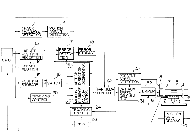
Fig. 1 is a block diagram showing the structure of
an information recording/reproducing apparatus according
to an embodiment of the present invention. In this
embodiment, information is recorded and reproduced using
a so-called optical card as an optical information
recording medium. At the right side of Fig. 1, the
mechanical part of the apparatus is shown. A light beam
is focussed on the recording surface of an optical card
1.
The position of the light beam on the optical card 1
is detected by a tracking error detector 5 which detects
a reflected light as a tracking error signal. This
tracking error signal is supplied to a tracking
2U~0057
controller 25. A closed circuit is formed by the
tracking error detector 5, tracking controller 25, closed
switch 26, and an actuator 3. The actuator 3 performs a
so-called tracking control which controls an objective
lens (not shown) so as to make the tracking error have a
zero value, i.e., make the light beam always locate the
center of a track. The actuator 3 also performs a near
jump, i.e., jumping to a nearby track. The tracking
error signal is detected by the tracking error detector
5.
In the case of a far jump, the switch 26 is opened
to open the tracking control loop and stop the operation
of the actuator 3. A linear motor 6 then moves the
optical head whose motion speed is detected by sensing a
scale 7 with a sensor 8.
This apparatus constructed as above is controlled by
a CPU. CPU supplies the apparatus with a motion command
to control the apparatus. A position data reading unit 9
reads address data of the optical card as the position
data.
The circuit portion to be controlled by CPU will be
described.
A motion command from CPU is supplied to a target
position receiving unit 13 to write the target position
data in this unit 13. The position data written in this
unit 13 is supplied to an offset adder 14. CPU supplies
an offset addition command to this adder 14 so as to
avoid a track overrun near at the periphery of the card.
The resultant position data is then supplied to a motion
direction designating unit 21 and to a motion distance
calculating unit 22.
A present position data is also supplied to the
motion direction designating unit 21 and to the motion
distance calculating unit 22. The present position data
before the start of moving the optical head 4 is read
from the optical card 1 by the position data reading unit
9 and supplied to a position data storage unit 15. This
11 20800S7
stored data is used as the present position data before
the start of moving the optical head 4.
The present position data after the optical head 4
moved is detected by a track traverse detecting unit 11
and motion amount detector 12, and supplied via a switch
16 to the motion direction designating unit 21 and motion
distance calculating unit 22. The switch 16 selects data
from the motion amount detector 12 and position storage
unit 15.
An output of the motion direction designating unit
21 is supplied to a driver 32 to drive the optical head
4, and to the actuator 3 to drive the objective lens.
An output of the motion distance calculating means
22 is supplied to a tracking on/off circuit 24 because
this output determines whether the tracking control is
required or not. The tracking on/off circuit 24 turns on
or off the switch 26. An output of the motion distance
calculating means 22 is also supplied to a far jump
controller 23.
The far jump controller 23 then generates an
acceleration/deceleration pattern in accordance with the
tracking motion distance, and supplies it to an optimum
speed calculating unit 31. In this case, an error of the
far jump carried out at the preceding time and stored in
an error storage unit 18 is considered to generate the
acceleration/deceleration pattern.
The optimum speed calculating unit 31 is supplied
with the present speed from the present speed detector
33, and sends an acceleration/deceleration signal to the
driver 32 to drive a linear motor 6. An output of the
present speed detector 33 is also supplied to the
tracking on/off circuit 24 so that when the linear motor
6 is decelerated-sufficiently, the tracking control
starts.
An output of the tracking on/off circuit 24 is
supplied to the error detector 17 so as to use it in
generating a far jump completion signal. Specifically,
20BDQS7
the error detector 17 calculates a difference between the
target position at the time of the far jump completion
and the present position, the difference being supplied
to the error storage unit 18 and to the far jump
controller 23.
Fig. 2 is a flow chart illustrating the operation of
the apparatus shown in Fig. 1. The operation of the
apparatus will be described with reference to this flow
chart.
CPU issues a motion command to write the position
data of a target track in the target position receiving
unit 13 (step Sl). At step S2, CPU checks whether the
target track is near at the card periphery and whether an
offset addition is required. If necessary, at step S3
the offset adder 14 adds an offset to the target position
to avoid a track overrun.
Thereafter, at step S4 the data previously written
in the position storage unit 15 by the position data
reading unit 9 is supplied via the switch 16 to the
motion direction designating unit 21 and motion distance
calculating unit 22. At step S5 the motion direction is
determined, and at step S6 a motion distance is
calculated.
The far jump controller 23 judges from the magnitude
of the obtained motion distance whether a far jump is
required (step S7). If a far jump is required, at step
S8 the far jump controller 23 determines an
acceleration/deceleration pattern while considering the
previous error stored in the error storage unit 18. An
output of the tracking on/off unit 24 opens the switch 26
to turn off the tracking control (step S9).
In this state, at step S10 the optimum speed
calculating unit 31 activate the driver 32 to drive the
linear motor 6, in accordance with the determined
acceleration/deceleration pattern. Acceleration
continues before half the motion distance (step Sll). At
half the motion distance, the optimum speed calculating
20800~ 7
unit 31 starts a deceleration at step S12. It is checked
at step S13 whether the deceleration has been made
sufficiently. If sufficient, at step S14 the tracking
control starts.
A position error at the time when the far jump
operation transits to the tracking control, is detected
by the error detector 17 at step S15, and stored at step
S16 in the error storage unit 18.
If the target position has been obtained at step
S17, the tracking controller 25 performs the tracking
control. If not, instead of an output from the position
storage unit 15, the switch 16 selects an output from the
motion amount detector 12 and sends it to the motion
direction designating unit 21 and motion distance
calculating means 22. In this manner, the motion
direction designating unit 21 and motion distance
calculating means 22 can know the present position which
is a difference between the motion amount generated by
the motion of the optical head and objective lens and the
initial position data given from the position data
reading unit 9.
The operations of steps S5 to S17 are repeated until
the target position is obtained. During these
operations, if the far jump controller 23 judges that the
operation to be carried out is not the far jump, in the
motion direction designated by the motion direction
designating unit 21 at step Sl9, the driver 32 operates
to perform a near jump at step S20. At step S21 it is
judged at step S21 if the target position has been
obtained. If not, the operation returns to step Sl9. If
obtained, the operation terminates.
Fig . 3 shows a n ex a m p le o f a n
acceleration/deceleration pattern to be used during the
speed control operation. This pattern has no constant
speed area, and the acceleration area is immediately
followed by the deceleration area. The time required for
14
0~ 7
the conventional constant speed is not necessary,
allowing to reach the target position faster.
The feeding mechanism (linear motor for the optical
head) is subject to an acceleration/deceleration control
by the circuit shown in Fig. 1 during the speed control
operation. During the other operation, the position of
the feeding mechanism is controlled by a position
controller (not shown). During the speed control
operation of the feeding mechanism, the actuator is not
controlled or it is under the tracking control. During
the position control operation of the feeding mechanism,
the actuator is under the position control.
Fig. 4 is a circuit diagram showing the structure of
an embodiment of a near jump controller for controlling
an optical head to jump to a nearby track according to
the present invention. Fig. 5 is a detailed circuit
diagram showing the structure of the track traverse
detector in the circuit shown in Fig. 4. Figs. 6A and 6B
are timing charts showing signal waveforms at various
circuit portions shown in Fig. 4.
Referring to Fig. 4, reference numeral 107
represents an optical i-nformation recording medium. A
light beam radiated through an objective lens 106 is
focussed on the optical card 107, and the reflected light
is applied to an optical detector 101 to form a tracking
error signal. This tracking error signal is amplified by
an amplifier 102 and supplied via a switch SW101 to a
tracking controller 104 to drive a tracking coil 105 for
driving the objective lens 106.
The tracking error signal is also supplied to a
track traverse detector 103 the details of which will be
later described with Fig. 5. The track traverse detector
103 shapes the tracking error signal into a rectangular
waveform to generate a track traverse detecting signal.
This track traverse detecting signal is supplied to
one input terminal of an exclusive OR EXOR100. Supplied
to the other input terminal of EXOR100 is a direction
16 2~00~
control signal which takes an L level when the objective
lens is moved in the forward direction and an H level
when it is moved in the backward direction. The
direction control signal is also used for opening and
closing a switch SW103. For the forward direction, the
switch SW103 opens to supply the positive power source
voltage +V to the left contact of the switch SW102 as
viewed in Fig. 4 via resistors R101 and R102. For the
backward direction, the switch SW103 closes to supply the
negative power source voltage -V to the left contact of
the switch SW102 via the resistor R102.
A signal at the Q output terminal of a flip-flop FF
is used for opening and closing the switch SW101. This
signal of an H level closes the switch SW101 to always
maintain the light beam at the center of a track, and the
signal of an L level opens the switch SW101. A signal at
an inverted Q output terminal of the flip-flop FF100 as
well as an output from EXOR100 is supplied to an AND gate
AND100 whose output is used for opening and closing the
switch SW102.
While the switch SW101 opens and the switch SW102
closes, a voltage corresponding to the state of the
switch SW103 is supplied to the tracking controller 104
via a conversion circuit made of a parallel circuit of a
resistor R104 and a serially connected resistor R105 and
capacitor C100. The tracking controller 104 flows a
current to the tracking coil 105 to start moving the
objective lens 106. When the switch SW102 opens under
this condition, the tracking controller 104 receives a
voltage signal of an inverted polarity and flows a
damping current to the tracking coil 105.
Fig. 5 shows the detailed structure of the track
traverse detector 103 shown in Fig. 4. The tracking
error signal applied to an input terminal IN is supplied
to the inverting terminal of a comparator CMP100 via an
integrator made of a resistor Rlll and capacitor Clll. A
reference signal Vref is applied to the non-inverting
16 2~ 8~ 0~ 7
input terminal of the comparator CMP100. The tracking
error signal is compared with the reference signal, and
the comparison result is outputted via a resistor R116 to
an output terminal OUT100. This reference voltage Vref
is a voltage divided by a serial circuit made of
resistors R115, R113, and R112.
The resistor R113 is a feedback element connected
between the non-inverting input terminal and output
terminal of the comparator CMP100. The reference voltage
Vref changes with an output voltage of the comparator
CMP100. As the feedback element of the comparator
CMP100, a serial circuit of a resistor R114 and capacitor
C112 is also connected to add an offset to an output of
the comparator CMP100.
Fig. 6(a) and (b) shows signal waveforms at various
circuit portions of Fig. 4 during the forward jump and
backward jump operations. The operation of the circuit
of Fig. 4 will be described with reference to these
waveforms shown in Fig. 6(a) and (b).
Forward Direction Jump
In order to determine the motion direction, the
direction control signal is set to an L level for the
forward direction jump. With the L level signal, the
switch SW103 opens, and so the positive voltage is
applied via the resistors R101 and R102 to the left
contact of the switch SW102. A track jump command of an
L level is issued at time tl and supplied to an inverted
reset terminal R of the flip-flop FF100. Therefore, the
Q output of the flip-flop FF100 takes an L level to open
the switch SW101 and stop the control of making the light
beam follow the center of a track. The inverted Q output
of the flip-flop FF100 takes an H level to close the
switch SW102 and supply a positive voltage to the
converter circuit made of the resistors R104, R105 and
capacitor C100. Accordingly, a drive current shown in
Fig. 6(a) flows in the tracking coil 105 to start moving
the objective lens 106 in the forward direction.
2~ D 5;7
As the objective lens 106 moves, the tracking error
signal changes from a zero level to a n~gative level and
from the zero level to a positive level. When the
tracking error signal becomes larger than the reference
value Vref, the track traverse detecting signal takes an
L level. Therefore, both the inputs to EXOR100 are L
level, and the output is L level. With an L level of the
output of EXOR100, the input conditions of the AND gate
AND100 are negated. Therefore, the AND gate AND100
supplies an L level signal to the switch SW102 to open
it.
Accordingly, the positive voltage having been
applied to the conversion circuit disappears at once so
that a current in the opposite direction will flow
through the tracking coil 105 to provide a fast damping.
This damping is carried out at time tl2 shown in Fig.
6(a). At time tl3 when the tracking error signal again
takes the zero level (when the light beam reaches the
center of the track), the track traverse detecting signal
takes an H level. With H and L level inputs, EXOR100
outputs an H level signal. The rising edge of this H
level signal is applied to a clock terminal of the flip-
flop FF100 so that the Q output of the flip-flop FF100
takes an H level to close the switch SW101 and lock the
objective lens 106 at that position. The inverted Q
output of the flip-flop FF100 takes an L level, and so
the input conditions of the AND gate AND100 are negated
to supply an L level signal to the switch SW102.
Backward Direction Jump
In order to determine the motion direction, the
direction control signal is set to an H level for the
backward direction jump. Therefore, the switch SW103
closes, and so the negative voltage is applied via the
resistor R102 to the left contact of the switch SW102.
When the switch SW102 closes, the direction of the
current flowing through the tracking coil 105 becomes
opposite to that during the forward direction jump. As
18 2~D~ 7
shown in Fig. 6(b), the tracking error signal changes in
the opposite direction to that shown in Fig. 6(a). The
operation is similar to that during the forward direction
jump except that the input conditions to EXOR100 are
reversed.
Fig. 7 is a circuit diagram showing another
embodiment of the present invention. In Fig. 7, IN201 to
IN203 represent input terminals. The input terminal
IN201 is supplied with a tracking error signal which is
detected with a detector assembled with an optical head
(not shown). The input terminal IN201 is supplied with a
tracking control signal, and the input terminal IN203 is
supplied with a direction control signal.
The tracking error signal applied to the input
terminal IN201 iS an analog signal whose polarity becomes
positive and negative in response to a track traverse of
the optical head. The tracking error signal is supplied
to the non-inverting input terminal of a comparator
CMP200 via an integrator made of a resistor R201 and
capacitor C201. Connected between the non-inverting
input terminal and output terminal of the comparator
CMP200 are a first feedback element constructed of a
resistor R203, a second feedback element constructed of a
serially connected resistor R204 and capacitor C202, and
a third feedback element constructed of a serially
connected resistor R205 and switch SW201. The first and
second feedback elements are always connected, and the
third feedback element is connected or disconnected by
the switch SW201 to change the feedback amount which
becomes large when the switch SW201 is closed, and small
when it is opened.
The tracking control signal applied to the input
terminal IN202 is an on/off signal which is directly
supplied to the switches SW201 and SW202. These switches
close during the on-tracking, and open during the off-
tracking. When the switch SW201 close, the resistor R205
is connected between the non-inverting input terminal and
19 2~8~0~7
output terminal of the comparator CMP200 to increase the
feedback amount between these terminals. When the switch
SW202 closes, the interconnection point between the
resistors R208 and R209 is grounded via the switch SW203,
so that the direction control signal applied from the
input terminal IN203 via the resistor R209 does not reach
the non-inverting input terminal of the comparator
CMP200.
The direction control signal applied to the input
terminal IN203 is an on/off signal which is directly
supplied to the switch SW203. The switch SW203 opens for
the forward direction, and closes for the backward
direction. The direction control signal is applied to
one input terminal of an exclusive OR EXOR200, and the
other input terminal is supplied with an output signal
from the comparator CMP200. The result of the logical
operation by EXOR200 is used in generating the track
traverse detecting signal.
The tracking error signal from the input terminal
IN201 is applied to the non-inverting input terminal of
the comparator CMP200. The non-inverting input terminal
is grounded vi-a a resistor R202, and connected via the
resistors R208 and R209 to the interconnection point
between a resistor 210 and switch SW203. The switch
SW203 opens and closes in response to the on and off of
the direction control signal. During the forward
direction control, the switch SW203 opens to supply a
positive voltage +V from a positive power source to the
non-inverting input terminal of the comparator CMP200 via
the resistors R208 and R209. During the backward
direction control, the switch SW203 closes to supply a
negative voltage -V from a negative power source to the
non-inverting input terminal of the comparator CMP200 via
the resistors R208 and R209.
An output terminal of the comparator CMP200 is
connected to the positive power source +V via a resistor
2080057
R206, and to the other input terminal of EXOR200 via an
integrator made of a resistor R207 and capacitor C203.
Figs. 8 to 10 show waveforms at various circuit
portions of the circuit shown in Fig. 7 during various
operations. Fig. 8 is for the forward direction near
jump, Fig. 9 is for the backward direction near jump, and
Fig. 10 is for the far jump, a comparison with a
conventional circuit operation being provided. In Figs.
8 to 10, waveforms indicated at (a) are of the tracking
error signal, waveforms indicated at (b) are of a slice
signal for slicing the tracking error signal, waveforms
indicated at (d) are of the signal at an output terminal
OUT, and waveforms indicated at (e) are of the output
signal of the comparator CMP200.
Three operation modes including a forward direction
near jump mode, backward direction near jump mode, and
far jump mode, are selected by the on/off operations of
the switches SW201 to SW203. In the forward near jump
mode, all the switches SW201, SW202, and SW203 are turned
off. In the backward near jump mode, the switches SW201
and SW202 are turned off and the switch SW203 is turned
on. In these two jump modes, the tracking control is
performed to correctly align the optical head on a track.
In the far jump mode, the switches SW201 and SW202 are
turned on (the switch SW203 may be turned on or off). In
the far jump mode, it is sufficient if the number of
tracks jumped by the optical head 4 can be correctly
known, and it is not important to check whether the
optical head is correctly on a track.
Forward Direction Near Jump
In the forward direction near jump mode, all the
switches SW201 to SW203 are open. Therefore, the first
feedback element made of the resistor R203 and the second
feedback element made of the serially connected resistor
R204 and capacitor C202 are inserted between the non-
inverting input terminal and output terminal of the
comparator CMP200. the non-inverting input terminal is
21 20%0057
connected to the positive power source +V via the
resistors R208 to R210. Accordingly, the potential or
slice level at the non-inverting input terminal of the
comparator CMP200 is a voltage obtained by dividing the
positive voltage +V by the serially connected resistors
R202, R208, R209, and R210. This voltage is a positive
value Vsl as indicated at (b) of Fig. 8.
The level of the tracking error signal at the input
terminal IN201 is checked by this positive high voltage.
Therefore, the output signal of the comparator CMP200 is
a correct rectangle as indicated at (e) of Fig. 8.
If the waveforms indicated at (e) and (d) of Fig. 8
are compared with a conventional track traverse detected
signal indicated at (c) of Fig. 8, it can be seen that
there is a distinct difference therebetween.
Specifically, the waveform indicated at (d) of Fig. 8 is
a correct rectangle, without having a pulsating signal C
at the disturbed area A of the signal near the zero level
indicated at (a) of Fig. 8 and a short duration rectangle
D at the shoulder B indicated at (a) of Fig. 8.
At the falling edge Po in the negative direction of
the rectangular signal indicated at (d) of Fig. 8,
information is written. The circuit constants are
selected and the slice level is set to detect this
falling edge correctly.
Neqative Direction Near Jump
In the negative direction near jump mode, the
switches SW201 and SW202 are off and the switch SW203 is
on. Therefore, a different point from the positive
direction near jump is that the negative power source -V
is supplied to the non-inverting input terminal of the
comparator CMP200 via the switch SW203 and resistors R208-
and R209. The slice level of the comparator CMP200 is a
negative value Vs2. The level of the tracking error
signal is checked using this slice level. A rectangular
signal indicated at (e) of Fig. 9 is generated
accordingly. As indicated at (d) of Fig. 9, the signal
2Q8~057
22
at the output terminal OUT200 is also a rectangular
signal.
Similar to the forward direction near jump explained
in Fig. 8, the waveform indicated at (d) of Fig. 9 is a
correct rectangle, without having a pulsating signal C at
the disturbed area A of the signal near the zero level
indicated at (a) of Fig. 9 and a short duration rectangle
D at the shoulder B indicated at (a) of Fig. 9.
At the rising edge Po in the positive direction of
the rectangular signal indicated at (d) of Fig. 9,
information is written. The circuit constants are
selected and the slice level is set to detect this
falling edge correctly.
Far Jump
In the far jump mode, the switches SW201 and SW202
are on. Therefore, the first to third feedback elements
are connected between the non-inverting input terminal
and output terminal of the comparator CMP200, providing a
large feedback amount. Different from the near jump, the
comparator CMP200 is not supplied with a voltage via the
resistors R208 and R209, and so the potential at the non-
inverting input terminal changes with a signal at the
output terminal.
Therefore, two positive and negative slice levels
Vsl' and Vs2' corresponding to the slice levels Vsl and
Vs2 indicated at (b) of Figs. 8 and 9 are obtained as
indicated at (b) of Fig. 10. The level of the tracking
error signal is checked by using these slice levels. A
rectangular signal indicated at (e) of Fig. 10 is
generated accordingly. A rectangular signal indicated at
(d) of Fig. 10 is also obtained at the output terminal
OUT.
Similar to the near jump explained in Figs. 8 and 9,
the waveform indicated at (d) of Fig. 10 is a correct
rectangle, without having a pulsating signal C at the
disturbed area A of the signal near the zero level
indicated at (a) of Fig. 10 and a short duration
~3 2~%0057
rectangle D at the shoulder B indicated at (a) of Fig.
10 .
The rectangular signal indicated at (d) of Fig. 10
is not so precise as the falling edge Po in the negative
5 direction or the rising edge Po in the positive direction
of the rectangular signal in the near jump mode.
However, the far jump control does not pose any problem
even if it is coarse, because the near jump control is
executed thereafter.
As described above, in both the near jump mode and
far jump mode, the track traverse detecting signal can be
obtained from the tracking error signal without being
adversely affected by noises contained in the tracking
error signal.