Note: Descriptions are shown in the official language in which they were submitted.
- 20~008~
MULTIPLE NARROW-LINE-CHANNEL FET HAVING
IMPROVED NOISE CHARACTERISTICS
BACKGROUND OF THE INVENTION
The present invention relates to a multiple narrow-
line-channel FET and a manufacturing method therefor.
One-dimensional devices are now being developed as next
generation devices succeeding MESFETs and HEMTs ~high electron
mobility transistors) in which electrons have degrees of
freedom of three and two, respectively with respect to their
movement. Among such one-dimensional-channel devices, a
multiple narrow-line-channel FET is known.
As shown in Fig. 5, the multiple narrow-line-channel
FET has a plurality of narrow-line channels 24a-24c called
"stripes" between a source 21 and a drain 23. A flow of
electrons (i.e., a current) in those channels 24a-24c is
controlled by a voltage applied to a gate electrode 22. Due to
its one-dimensional nature of electron transport, the multiple
narrow-line-channel FET is expected to have a large electron
mobility.
Fig. 6 is a sectional view taken along line Y-Y' in
Fig. 5. As is understood from Fig. 6, an electric field acting
on the channels 24a-24c from their side faces has an effect of
confining electrons within each of the channels 24a-24c.
Therefore, it is also expected that the short-channel effect
will be overcome. (The short-channel effect is a phenomenon in
2tl800~0
which it becomes difficult to control a very small current
flowing from the source to drain by the gate voltage.)
In Fig. 6, reference numeral 25 represents a GaAs
substrate; 26, undoped GaAs layer; 27, n+-type AlGaAs layer;
28, n~-type GaAs layer; and 29, electrons.
However, since the above conventional multiple narrow-
line-channel FET has gate metal at the sides of each channel
(stripe), the gate capacitance increases by a capacitance due
to depletion layers extending from the side faces of the
channels, so that the noise characteristics are deteriorated as
described below. The noise figure NF is given by the following
equation:
NF = 1 + K~f/fT)~gQ(Rs + Rg) ~---- (1)
where K: fitting constant, f: frequency, fT: cutoff frequency,
gm: transconductance, R9: source resistance, and Rg: gate
resistance. The cutoff frequency fT is expressed as:
fT = gQ/ 2~CgS I
and the capacitance due to the depletion layer increases a
gate-source capacitance Cg9. As a result, the cutoff frequency
fT is decreased, and the noise figure NF is increased as is
understood from equation (1).
SUMMARY OF THE INVENTION
The present invention has been made in view of the
above problem in the art, and has an object of reducing a
capacitance at side faces of channels of a multiple narrow-
-- 2
2080080
line-channel FET having one-dimensional channels, to thereby
improve its noise characteristics.
According to the invention, a multiple narrow-line-
channel FET comprises:
5a plurality of compound semiconductor layers having a
multilayer structure;
a plurality of first insulating layers formed in the
compound semiconductor layers at predetermined intervals;
a plurality of channel layers formed between the first
10insulating layers;
a gate electrode formed on the first insulating layers
and the channel layers so as to traverse those layers; and
source and drain electrodes formed on both sides of the
gate electrode.
15According to the invention, a manufacturing method of
a multiple narrow-line-channel FET comprises the steps of:
forming sequentially a plurality of compound
semiconductor layers;
injecting ions into the compound semiconductor layers
20in areas spaced from each other at predetermined intervals to
form a plurality of ion-injected insulating layers and to leave
a plurality of channel layers between the ion-injected
insulating layers;
forming a gate metal electrode on the ion-injected
25insulating layers and the channel layers so as to traverse
those layers; and
. 2~80080
forming source and drain metal electrodes on both sides
of the gate metal electrode.
Further, according to the invention, a manufacturing
method of a multiple narrow-line-channel FET comprises the
steps of:
forming sequentially a plurality of compound
semiconductor layers;
mesa-etching the compound semiconductor layers to form
a plurality of recesses spaced from each other at
predetermined intervals and to leave a plurality of channel
layers between the recesses;
filling the recesses by an insulating material to form
a plurality of first insulating layers;
forming a gate metal electrode on the first insulating
layers and the channel layers so as to traverse those layers;
and
forming source and drain metal electrodes on both sides
of the gate metal electrode.
Accordingly, in a further aspect, the present invention
relates to a multiple narrow-line-channel FET, comprising:
a plurality of compound semiconductor layers having a
multilayer structure and having different compositions;
a plurality of channel layers formed in the plurality
of compound semiconductor layers;
a plurality of first insulating layers formed in the
compound semiconductor layers of different compositions at
l~ ~
'2 208008 0
predetermined intervals between the channel layers;
a gate electrode formed on the compound semiconductor
layers so as to traverse the channel layers and the first
insulating layers; and
source and drain electrodes formed on both sides of the
gate electrode.
In a further aspect, the present invention relates to
a manufacturing method of a multiple narrow-line-channel FET,
comprising the steps of:
forming sequentially a plurality of compound
semiconductor layers by varying the compositions of the
respective compound semiconductor layers so that the plurality
of compound semiconductor layers so that the plurality of
compound semiconductor layers have different compositions;
forming a plurality of channel layers by injecting ions
into the compound semiconductor layers in areas spaced from
each other at predetermined intervals to form a plurality of
ion-injected insulating layers and to leave a plurality of
channel layers between the ion-injected insulating layers;
forming a gate metal electrode on the compound
semiconductor layers so as to traverse the channel layers and
the insulating layers; and
forming source and drain metal electrodes on both sides
of the gate metal electrode.
- 4a -
s
I~ i
~ ~ ~ 8 ~ 0 8 ~
BRIEF DESCRIPTION OF THE DRAWINGS
Fig. 1 is a sectional view of a multiple narrow-line-
channel FET according to a first embodiment of the present
invention;
Fig. 2(a) is a sectional view showing a manufacturing
method of the FET of Fig. 1;
Figs. 2(b)-2(d) are plan views showing the manufacturing
method of the FET of Fig. 1;
- 4b -
~8Q~8 0
Fig. 3 is a sectional view of a multiple narrow-line-
channel FET according to a second embodiment of the invention;
Fig. 4 is a sectional view of a multiple narrow-line-
channel FET according to a third embodiment of the invention;
Fig. 5 is a plan view of a conventional multiple
narrow-line-channel FET; and
Fig. 6 is a sectional view taken along line Y-Y' in
Fig. 5.
DESCRIPTION OF THE PREFERRED EMBODIMENTS
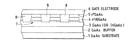
Fig 1 is a sectional view of a multiple narrow-line-
channel FET according to a first embodiment of the present
invention. In the figure, reference numeral 1 represents a
GaAs substrate; 2, GaAs buffer layer; 3, GaAs (or InGaAs)
layer; 4, n+-type AlGaAs layer (or n+-type AlInGaAs layer); 5,
n+-type GaAs layer; 6, gate electrode of aluminum etc. The
main features of this embodiment are that ion-injected
insulating layers 8 are formed at predetermined intervals (not
necessarily at the same intervals) to restrict channels
(stripes) 7, and that the gate electrode 6 is formed on the
channels 7 and ion injection layers 8. The width of each
stripe 7 is selected to be within the range of 100-800 A, as a
result of which each channel 7 can be regarded as one-
dimensional.
Since there exists no gate metal at the sides of each
channel 7, almost no depletion layer develops from its side
faces unlike the conventional case. As a result, the gate-
-
- 2080080
source capacitance Cg8 does not take an unduly large value, and
the noise figure NF is reduced.
Figs. 2(a)-2(d) illustrate a manufacturing method of
the FET of Fig. 1. First, as shown in Fig. 2(a), a GaAs buffer
layer 2, a GaAs (or InGaAs) layer 3, an n+-type AlGaAs layer
(or n+-type AlInGaAs layer) 4 and an n+-type GaAs layer 5 are
sequentially formed on a GaAs substrate 1. Then, as shown in
Fig. 2(b), a resist film 9 having openings 9a-9c are formed on
the n+-type GaAs layer 5. Ions of, e.g., oxygen, hydrogen or
boron are injected via the resist film 9.
After removing the resist film 9, ohmic contact metal
for the source and drain electrodes is deposited by evaporation
via a pattern 10 as shown in Fig. 2(c), and then the pattern 10
is lifted off. Then, another pattern for a gate electrode 6 is
formed. After gate metal (e.g., Al, Ti/Pt/Au and WSi/Au) is
deposited by evaporation, the pattern is lifted off. Recess
etching for the gate electrode 6 may be performed additionally.
In this manner, an FET as shown in Fig. 2(d) is
produced. Fig. 1 is a sectional view taken along line X-X' in
Fig. 2(d). In Fig. 2(d), reference numeral 11 represents the
ohmic contact metal for the source and drain electrodes.
Fig. 3 shows a second embodiment of the invention, in
which insulator layers 12 are provided instead of the ion
injection layers 8 of Fig. 1. The remaining constitution is
the same as the first embodiment of Fig. 1. The insulator
layers 12 may be made of SiO2, silicon nitride, alumina, etc.
~ ~8~08 ~
The FET of Fig. 3 is manufactured as follows. First,
the semiconductor layers 1-5 are formed on the GaAs substrate
l by epitaxial growth as in the case of Fig. 2(a). Next, mesa-
etching is performed using the resist film 9 of Fig. 2(b) as a
mask. Using the same mask, an insulator film (e.g., a nitride
film) is deposited at a low temperature into recesses formed by
the mesa-etching. This deposition of the insulator film can be
performed with a CVD apparatus that uses a microwave. Then,
the resist layer 9 and the insulator film deposited thereon are
removed by a lift-off process. Thereafter, the processes of
Figs. 2(c) and 2(d) are performed.
Fig. 4 shows a third embodiment of the invention. In
the third embodiment, first the ion injection layers 8 are
formed in the same manner as the first embodiment of Fig. l,
then insulator layers 13 are formed on the respective ion
injection layers 8 so as to project upward, and finally a gate
electrode 6' is formed on the surface that includes the
insulator layers 13.
A production method for the FET of the third embodiment
can be the same as first embodiment until formation of the
injection layers 8. Thereafter, an insulator film is deposited
and partially removed by a lift-off process. The gate
electrode 6' may be formed by the process of Fig. 2(d).
In the third embodiment of Fig. 4, the insulator layers
13 may be formed on the insulator layers 12 of Fig. 3, instead
of the injection layers 8 of Fig. 1. (The insulator layers 12
-- 208ao8~
is formed by depositing an insulating material into the mesa-
etched recesses.)
In each of the above embodiments, thicknesses of the
semiconductor layer (GaAs or InGaAs layer) 3 and the
semiconductor layer (n+-type AlGaAs layer or n'-type AlInGaAs
layer) 4 are selected to be 80-160 A and 200-400 A,
respectively.
As described above, according to the invention, since
there exists no gate metal at the sides of the channels,
almost no depletion layer develops from the side faces of each
channel. As a result, the gate capacitance can be reduced as
much, and high-quality, i.e., low-noise multiple narrow-line-
channel FET can be realized.