Note: Descriptions are shown in the official language in which they were submitted.
~A
CFO 8745 ~
-- 1 --
2~0~
l ELECTRON-EMITTING DEVICE, AND ELECTRON BEAM-GENERATING
APPARATUS AND IMAGE-FORMING APPARATUS
EMPLOYING THE DEVICE
5 BACKGROUND OF THE INVENTION
Field of the Invention
The present invention relates to a cold-
cathode type of electron-emitting device. The present
invention also relates to an electron beam-generating
apparatus, and an image-forming apparatus employing
the electron-emitting device.
Related Background Art
Cold cathode devices are known as devices
capable of emitting electrons with a simple structure.
For example, a cold cathode device is reported by M.I.
Elinson (Radio Eng. Electron Phys., vol. 10, pp. 1290-
1296 (1965~). These devices are based on the
phenomenon that electrons are emitted by flowing
electric current in parallel through a thin film of
small area formed on a substrate. Such devices are
called generally surface-conduction type electron-
emitting devices. The surface-conduction type
electron-emitting devices include the ones using a
thin SnO2(Sb) film developed by M.I. Elinson as
mentioned above; the ones using a thin Au film (G.
Dittmer: "Thin Solid Films", vol. 9, p. 317, (1972));
-- 2 --
2~09~
l and the ones using a thin ITO film (M. Hartwell and
C.G. Fonstad: IEEE Trans. ED Conf., p. 519 (1975)).
A typical construction of the surface
conduction type electron-emitting device is shown in
Fig. 30. This device comprises electrodes 82, 83 for
electric connection, a thin film 85 formed from an
electron-emitting material, a substrate (insulating
base) 81, and an electron-emitting portion 84.
Conventionally, in such a surface conduction type
electron~emitting device, the electron-emitting
portion is formed by electric current-heating
treatment called "forming". In this treatment,
electric voltage is applied between the electrode 82
and the electrode 83 to flow electric current through
the thin film 85 and to destroy, deform, or denature
locally the thin film 85 by utilizing Joule heat
generated. Thereby, the electron-emitting portion 84
which has high electric resistance is formed, thus the
function of electron emission being obtained. Here
the state of the high electric resistance results from
discontinuity of the thin film 85 in which cracks of
0.5 to 5 ~m long are formed locally and the cracks
have an island structure therein. The island
structure means a state of the film that the film
contains fine particles of several tens of angstroms
to several microns in diameter and the particles are
~;,; :
- 3 - 2~QQ ~ 2
1 discontinuous but the film is electrically continuous.
In conventional surface conduction type electron-
emitting device, voltage is applied to the
aforementioned discontinuous high-resistance film
through the electrodes 82, 83 to flow current at the
surface of the device, thereby electron being emitted
from the fine particles.
A novel surface conduction type electron-
emitting device in which electron-emitting fine
particles are distributed between electrode was
disclosed by the inventors of the present invention in
Japanese Patent Application Laid-Open Nos. Hei-1-
200532 and Hei-2-56822. This electron-emitting device
has advantages that (1) high electron-emitting
efficiency can be obtained, (2) the device can be
readily prepared because of its simple construction,
(3) many devices can be arranged on one and the same
substrate, and so forth. Fig. 31 shows a typical
construction of such a surface conduction type
electron-emitting device, which comprises electrodes
82, 83 for electric connection, an electron-emitting
portion 86 having electron-emitting fine particles
dispersed therein, and a substrate 81.
In recent years, attempts are made to use the
aforementioned surface conduction type electron-
emitting device for an image-forming apparatus. One
--4-- 2 ~
1 example is shown in Fig. 32, which illustrates an
image-forming apparatus having a number of the
aforementioned electron-emitting devices arranged
therein. The apparatus comprises wiring electrodes
92, 93, electron-emitting portions 94, grid electrodes
95, electron-passing holes 96, and an image-forming
member 97. This image-forming member is made of a
material such as fluorescent materials and resist
materials which causes light-emission, color change,
electrification, denaturing or like change on
collision of electrons. With this image-forming
apparatus, the linear electron sources having a
plurality of electron-emitting portions 94 arranged
between the electrodes 92, 93, and grid electrodes 95
are driven in XY matrix, and electrons are made to
collide against the image-forming member 97 in
correspondence with information signals to form an
image.
The electric characteristics (current-voltage
characteristics) of conventional surface conduction
type of electron-emitting devices are explained by
reference to Fig. 6. In conventional electron-
emitting devices, electron emission increases rapidly
from a certain device voltage Ve (voltage applied to
the device) with increase of the device voltage, and
at a device voltage Vd, sufficient electron beam comes
2~0~2
l to be emitted: for example, sufficient electron beam
for forming image in the above-mentioned image-forming
apparatus. The device current If (current which flows
in the device) increases with the device voltage, and
the rate of the increase becomes larger at around the
device voltage Ve. In such conventional devices
generally, strong ineffective current, which is
useless for electron emission, flows as shown in Fig.
6. The ratio of the ineffective current to the device
current If rises in some cases to as much as about 50
%. Such increase of the ineffective current will
cause increase of power consumption in driving the
electron-emitting device, and increase of heat
generation in the electron-emitting device to
deteriorate electron-emitting characteristics
(electron-emission efficiency, electron-emission
stability, etc. Further the increase of the
ineffective current gives rise to the problems, when
the electron-emitting device in which the ineffective
current is remarkable is used for an image-forming
apparatus: 1) the ineffective current flows to wiring
electrodes to cause voltage drop, whereby the quantity
of electron emission varies with the electron-emitting
devices, and 2) the ineffective current varies
depending on the kind of the image (namely, difference
in inputted information signal) to cause voltage drop
-- 6
2 ~
1 in wiring electrode, whereby quantity of the emitted
electrons varies. Such disadvantageous phenomena
further cause lowering of contrast and sharpness of
the formed image; and in particular, in the case where
the formed image is a fluorescent image, bring about
variation and change of luminance of the fluorescent
images, which makes it difficult to obtain fineness of
the image and to enlarge a picture screen, and further
increase the power consumption.
SUMMARY OF THE INVENTION
An object of the present invention is to
provide an electron-emitting device and an electron
beam-generating apparatus in which ineffective current
is extremely weak.
Another object of the present invention is to
provide an electron-emitting device and an electron
beam-generelting apparatus which are excellent in
electron emission characteristics such as electron-
emission efficiency, and electron-emission stability,
and which consumes less electric power.
A further object of the present invention is
to provide an electron beam-generating apparatus in
which ineffective current is extremely weak in a whole
apparatus, and which gives an image with high contrast
and high sharpness with less power consumption, in
- 7 ~
1 particular an electron beam-generating apparatus
capable of forming a luminescent image with extremely
low variation and low fluctuation of luminance.
According to an aspect of the present
invention, there is provided an electron-emitting
device having an electron-emitting region between
electrodes on a substrate, the electron-emitting
region containing fine particles dispersed therein at
an areal occupation ratio of the fine particles
ranging from 20 % to 75 % of the electron emitting
region.
According to another aspect of the present
invention, there is provided an electron-emitting
device having an electron-emitting region hetween
electrodes on a substrate, the electron-emitting
region containing the fine particles dispersed therein
at gaps of from 5 A to 100 A and having average
particle diametsr of from 5 A to 1000 A.
According to still another aspect of the
present invention, there is provided an electron-
emitting device having an electron-emitting region
between electrodes on a substrate, the electron-
emitting region containing fine particles dispersed
therein at an areal occupation ratio of the fine
particles ranging from 20 % to 75 % of the electron-
emitting region, and the fine particles being
2~a~2
l dispersed at gaps of from 5 A to 100 A and having
average particle diameter of from 5 A to 1000 A.
According to a further aspect of the present
invention, there is provided an electron-emitting
device having an electron-emitting region between
electrodes on a substrate, the voltage application
length in the electron-emitting region ranging from 5
A to 300 A .
According to a still further aspect of the
present invention, there is provided an electron-
emitting device having an electron-emitting region
between electrodes on a substrate, the electric field
strength in the electron-emitting region being not
less than 107 V/cm.
: 15 According to a further aspect of the present
invention, there is provided an electron-beam
generating apparatus, comprising a plurality of the
above-specified electron emitting devices and a
modulation means for modulating the electron beams
emitted from the electron-emitting devices in
accordance with information signals.
According to a still further aspect of the
present invention, there is provided an image-forming
apparatus, comprising a plurality of the above-
specified electron-emitting devices, a modulation
means for modulating the electron beams emitted from
- 9 2~1)D~,
1 the electron-emitting devices in accordance with
information signals, and an image-forming member for
forming image on irradiation of electron beams.
According to a further aspect of the present
invention, there is provided an image-forming
apparatus, comprising a plurality of the above-
specified electron-emitting devices, a modulation
means for modulating the electron beams emitted from
the electron-emitting devices in accordance with
information signals, and light-emitting member for
emitting light on irradiation of electron beams.
According to a still further aspect of the
present invention, there is provided an image-forming
apparatus, comprising a plurality of the above-
specified electron-emitting devices, a modulation
means for modulating the electron beams emitted from
the electron-emitting devices in accordance with
information signals, light-emitting member for
emitting light on irradiation of electron beams, and a
recording member for recording an image on irradiation
of light from the light-emitting member.
According to a further aspect of the present
invention, there is provided an image-forming
apparatus, comprising a plurality of the above-
specified electron-emitting devices, a modulation
means for modulating the electron beams emitted from
lo- 2~ 2
l the electron-emitting devices in accordance with
information signals, light-emitting member for
emitting light by irradiation of electron beams, and a
supporting means for a recording member for recording
an image by irradiation of light from the light-
emitting member.
BRIEF DESCRIPTION OF THE DRAWINGS
Fig, 1 is a plan view illustrating
schematically an electron-emitting device of the
present invention.
Fig. 2 is a sectional view of the electron-
emitting device at A-A' in Fig. 1.
Fig. 3 is a sectional view of the electron-
emitting device at B-B' in Fig. 2.
Fig. 4A is an SEM photograph of an electron-
emitting region between electrodes of an electron-
emitting device of the present invention
(magnification: X30,000).
Fig. 4B is a sketch of an SEM photograph of an
electron-emitting region of Fig. 4A (plan view~.
Fig. 5A is an enlarged SEM photograph of an
electron-emitting region of the electron-emitting
device of Fig. 4 (magnification: x150,000).
Fig. 5B is an enlarged SEM photograph of an
electron-emitting region of the electron-emitting
- 11 - 2Q800~2
l device of Fig. 4 (magnification: x800,000).
Fig. 5C is a sketch of the enlarged SEM
photograph of an electron-emitting region of Fig. 5A
(plan view).
Fig. 6 shows current-voltage relation of a
conventional electron-emitting device.
Fig. 7 shows current-voltage relation of an -
electron-emitting device of the present invention.
Fig. 8A is an SEM photograph (magnification:
X150,000) to explain the method for measuring the
voltage application length of the electron-emitting
device of the present invention.
Fig. 8B is a sketch of the SEM photograph of
Fig. 8A.
Fig. 9A is another SEM photograph
(magnification: x150,000) to explain the method for
measuring the voltage application length of the
electron-emitting device of the present invention.
Fig. 9R is a sketch of the SEM photograph of
Fig. 9A.
Fig. 10 is a drawing to explain the method for
measuring the voltage application length of the
electron-emitting device of the present invention.
Figs. llA to llC are drawings to explain a
method for preparing the electron-emitting device of
the present invention (sectional view).
- 12 - 2~8~
l Fig. 12 shows a wave form of the pulse voltage
on forming treatment of an electron-emitting device of
the present invention.
Fig. 13 shows another wave form of the pulse
voltage on forming treatment of an electron-emitting
device of the present invention.
Figs 14A to 14E are drawings to explain a
method for preparing the electron-emitting device of
the present invention (sectional view).
Figs. 15A to 15D are drawings to explain a
method for preparing the electron-emitting device of
the present invention (sectional view).
Fig. 16 illustrates schematically the
construction of the measurement apparatus of electron
emission characteristics of an electron-emitting
device.
Fig. 17 is a perspective view illustrating
schematica:lly an electron beam-generating apparatus of
the present invention.
Fig. 18 is a perspective view illustrating
schematically another electron beam-generating
apparatus of the present invention.
Fig. 19 is a perspective view illustrating
schematically still another electron beam-generating
apparatus of the present invention.
Fig. 20 is a perspective view illustrating
- 13 - 2~ 2
l schematically still another electron beam-generating
apparatus of the present invention.
Fig. 21 is a perspective view illustrating
schematically still another electron beam-generating ~
5 apparatus of the present invention.
Fig. 22 is a perspective view illustrating
schematically an image-forming apparatus of the
present invention.
Fig. 23 is a perspective view illustrating
10 schematically another image-forming apparatus of the
present invention.
Fig. 24 is a perspective view illustrating
schematically still another image-forming apparatus of
the present invention.
Fig. 25 is a perspective view illustrating
schematically still another image-forming apparatus of
the present invention.
Figs. 26A and 26B illustrate schematically an
image-forming apparatus (optical printer) of the
20 present invention.
Fig. 27 illustrates schematically another
image-forming apparatus (optical printer) of the
present invention.
- Fig. 28 illustrates schematically an image
forming apparatus provided with a supporting member of
the present invention (assembling drawing).
- 14 - 2~ 2
1 Fig. 29 is a sectional view of the apparatus
of Fig. 28.
Fig. 30 is a plan view illustrating
schematically construction of a conventional electron-
emitting device.
Fig. 31 is a plan view illustratingschematically construction of another conventional
electron-emitting device.
Fig. 32 is a perspective view of a
conventional image-forming apparatus.
DESCRIPTION OF THE PREFERRED EMBODIMENT
The electron-emitting device of the present
invention is described below in detail. Firstly, the
characteristic portion of the electron-emitting device
is explained by reference to Fig, 1 (plan view), Fig.
2 (sectional view at A-A' in Fig. 1), and Fig. 3
(sectional view at B-B' in Fig. 2). In Figs. 1 to 3,
the numeral 1 denotes an insulating substrate; 2 and
3, each an electrode; 5, an electron-emitting region;
4, a fine particle film having an electric resistance
lower than that of the electron-emitting region 5; and
6, a fine particle dispersed in the electron-emitting
region 5. The electron-emitting device of the present
invention is required essentially to have an electron-
emitting region 5 having fine particles 6 dispersed
- 15 - 2~800~2
l therein, and electrodes 2 and 3 to apply voltage to
the interior of the region 5. The electron-emitting
device of the present invention serves in such a
mechanism that electrons pass (or current flows)
through the electron-emitting region by application of
voltage between the electrodes 2 and 3, and the
electrons are emitted out from the gap formed by the
fine particles 6 (or spacing between the fine
particles) in the region. The fine particle film 4
having lower resistance is not an essential
requirement in the present invention, but is preferred
to improve further the electrical contact between the
electron-emitting region 5 and the electrodes 2 and 3.
The electron-emitting region and the fine particles
constituting the fine particle film 4 are both made of
an electroconductive material.
In addition to the above essential
requirement, the electron-emitting device of the
present invention has to satisfy further another
requirement shown below, and is classified into two
types of embodiments according to the requirement. It
is described in detail.
In the one type of embodiment of the electron-
emitting device, the areal occupation ratio of of the
fine particles is in the range of from 20 to 75 ~ in
the electron-emitting region 5. Fig. 4A, Fig. 5A, and
- 16 - 20~092
l Fig. 5B are SEM (scanning electron microscope)
photographs of an electron-emitting region of an
electron-emitting device of the present invention
prepared as examples described later. Fig. 4B and
Fig. 5C are sketches of the SEM photographs. Fig. 4A
and Fig. 4B shows a view of the region A-A' of Fig. 2
observed from the top. Fig. 5A and Fig. 5C shows a
view of the region A-A' of Fig. 2 observed from the
top. Fig. 5B and the dotted-line region in Fig. 5C
correspond to the enlarged view of the electron-
emitting region 15 observed with SEM of high
magnification. The numerals 12 and 13 denote
electrodes; 14, a fine particle film; 15, an electron-
emitting region; and 16 a fine particle dispersed in
the electron-emitting region 15. The areal occupation
ratio in the present invention means the value
measured as follows. As shown by the dotted-line area
in Fig. 5C, the SEM image of the inside of the
electron-emitting region 15 of the element is taken at
a magnification such that 10 to 1000 fine particles
are observed (Fig. 5B). (An STM image (scanning
tunnel microscopy image) may be used instead of the
SEM image.) With the SEM image, the ratio of the
total area of the fine particles to the whole dotted-
line area is measured. This measurement is practiced
throughout the entire area of the electron-emitting
- 17 2~ 2
l region 15. The average of the measured values is the
areal occupation ratio of the fine particles
In the electron-emitting device of the present
invention, the relations of the areal occupation ratio
of the fine particles with the aforementioned
ineffective current flowing in the device, and with
the electron-emitting characteristics of the device
are considered as below by the inventors of the
present invention. If the areal occupation ratio of
the fine particles is excessively large, the ratio of
the aforementioned gap to the entire electron-emitting
region is extremely small, and the the electron-
emitting region behaves as a continuous film.
Therefore, the quantity of electrons flowing through
the continuous film is larger than the quantity of
electrons emitted from the gap. As the results, the
the ineffective current becomes stronger, and quantity
of the emitted electrons decreases. On the other
hand, if the areal occupation ratio is extremely
small, the ratio of the aforementioned gap to the
entire electron-emitting region is excessively large,
and the higher voltage is required for electron
emission. Therefore, a phenomenon occurs that
electrons once emitted are pulled back to the
electrode. As the results, the ineffective current
becomes stronger, and the quantity of the emitted
- 18 - 2~ 2
1 electrons decreases also in this case.
After comprehensive study on the basis of the
above considerations, it was found by the inventors of
the present invention that, if the areal occupation
ratio of the fine particles is in the range of from 20
to 75 %, more preferably from 35 to 60 %, the
ineffective current of the electron-emitting device is
effectively made extremely small, and the quantity of
electron emission is increased, and further thereby
the electron-emission efficiency and the electron-
emission stability are improved effectively.
Consequently, the present invention has been
completed.
In this first embodiment of the present
invention, the average particle diameter of the fine
particles dispersed in the electron-emitting region is
adjusted preferably to be in the range of from 5 to
300 A, more preferably 5 to 80 A. With the average
diameter within this range, the ineffective current
flowing through very large particles can be
suppressed, the ineffective current in the whole
device can further be reduced, and the electron
emission efficiency and the electron emission
stability (in particular, flickering of electron
emission) are improved more.
In the other type of embodiment of the
-- 19 --
2Q~92
l electron-emitting device of the present invention, the
gap between the fine particles 6 in the electron-
emitting region 5 is in the range of from 5 to 100 A,
and the average particle diameter of the fine
particles is in the range of from 5 to 1000 A. The
gap between the fine particles in the present
invention means the spacing of particles as shown by
the symbol S in Fig. 3. The gap S of the fine
particles and the average particle diameter t are
measured as follows. As shown by the dotted-line area
in Fig. 5, the SEM image of the inside of the electron-
emitting region 15 (photograph) of the element is
taken at a magnification such that 10 to 1000 fine
particles are observed. (An STM image (scanning
tunnel microscopy image) may be used instead of the
SEM image.) With the SEM image, the gaps S and the
diameters t of all the fine particles are measured.
This measurement is practiced throughout the entire of
the electron-emitting region 15. The respective
average of the measured values are the gap and the
average particle diameter of the fine particles.
In the electron-emitting device of the present
invention, the dependence of the ineffective current
flowing in the device and the electron emission
characteristics of the device on the fine particle gap
and the average diameter are considered as below by
- 20 -
1 the inventors of the presen-t invention. If the the
average particle diameter is excessively large and the
fine particle gap is extremely small, the ratio of the
aforementioned gap to the entire electron-emitting
region is too small, and the the electron-emitting
region behaves as a continuous film. Therefore, the
quantity of electrons flowing through the continuous
film is larger than the quantity of electrons emitted
from the gap. As the results, the the ineffective
current becomes large, and quantity of the emitted
electrons decreases. On the other hand, if the the
average particle diameter is extremely small and the
gap of the fine particles is extremely large, the
ratio of the aforementioned gap to the entire electron-
emitting region is too large, and the higher voltageis required for electron emission. Therefore, a
phenomenon occurs that electrons once emitted are
pulled back to the electrode. As the results, the
ineffective current becomes large, and the quantity of
the emitted electrons decreases also in this case.
On the basis of the above considerations,
comprehensive studies were made by the inventors of
the present invention, and it was found that, if the
gap of the fine particles is adjusted to be within the
range of from 5 to 100 A, preferably 5 to 50 ~, the
ineffective current of the electron-emitting device is
- 21 -
2~0~2
1 effectively made extremely small, and the quantity of
electron emission is increased, and further thereby
the electron emission efficiency and the electron
emission stability are improved effectively.
Consequently, the present invention has been
completed. In this second embodiment of the present
invention, the average particle diameter of the fine
particles dispersed in the electron-emitting region is
adjusted preferably to be in the range of from 5 to
300 A, more preferably 5 to 80 A from the same reason
as in the above-described first embodiment.
Two types of embodiments of the electron-
emitting device of the present invention are described
above. The electron-emitting device which meets
simultaneously the both requirements of the two types
of embodiments is more preferable in the present
invention. That is, if the the areal occupation ratio
in the electron-emitting region is from 20 to 75 %,
the gap of the particles is from 5 to lU0 A, and the
average particle diameter of the fine particles is
from 5 to 1000 A, then the electron-emitting device is
improved in comparison with each of the above
embodiments in reducing the ineffective current in the
device and is superior in electron emission quantity,
electron emission efficiency, and electron emission
stability ~prevention of flic~ering of electron
- 22 -
2 ~ 2
l emission), and further the device is driven with lower
voltage and has longer life. The above effects are
more remarkable if the areal occupation ratio is from
35 to 60 %, and the particle gap is from 5 to 50 A.
The effects are still more remarkable if the average
particle diameter is from 5 to 300 A, more preferably
5 to 80 A .
The methods for controlling the areal
occupation ratio, the fine particle gap, and the fine
particle diameter are described below. The control of
these parameters were practiced as follows. The gap
between the electrodes was set in the range of from
0.2 to 5 ~m. An electroconductive film having sheet
resistance of from 3 x 10³ Q/cm2 to 107 Q/cm2 was
formed by placing electroconductive particles of from
5 to 100 A in particle diameter in dispersion between
the electrodes. To the electroconductive film, a
specified wave form of voltage pulse was applied
through the electrodes. The applied voltage pulse is
suitably decided depending on the shape of the
electrodes, the material of tha electroconductive
film, and the material of the substrate. The ma~erial
of the electroconductive particles includes metals
such as Pd, Nb, Mo, Rh, Hf, Ta, W, Re, Ir, Pt, Ti, Au,
Ag, Cu, Cr, Al, Co, Ni, Fe, Pb, Cs, and Ba; borides
such as LaB6, CeB6, HfB4, and GdB4; carbides such as
- 23 - 2~8~
l TiC, ZrC, HfC, TaC, SiC, and WC; nitrides such as TiN,
ZrN, and HfN; metal oxides such as PdO, Ir2O3, SnO2,
and Sb2O; semiconductors such as Si, and Ge; carbon,
Ag, Mg, and the like. The above method is preferred
in controlling the parameters.
The large ineffective current of conventional
electron-emitting device as described above, was
further studied by the inventors of the present
invention. As the results, it was found that the
strength of the ineffective current flowing through
the electron-emitting device varies depending on the
size of the region where the voltage for driving the
device is effectively applied (the size being referred
to as "voltage application length"). It was further
found that the ineffective current can be suppressed
to extremely small by adjusting the voltage
application length within a certain range, the
ineffective current of the device being negligible at
the voltage application length of from 5 to 300 A,
preferably 5 to 50 A. The voltage application length,
in more detail, means a length of the region where the
voltage is effectively applied as described above in
the electron-emitting device. In this region, voltage
drops substantially but outside the region, the
voltage does not drop substantially.
The voltage application length is measured as
- 24 - 2~ 2
l below. Fig. 8A is an SEM photograph of an area
between the electrodes on application of voltage to an
electron-emitting device of the present invention.
Fig. 8B is a sketch of the SEM photograph of Fig. 8A.
Fig. 9A is an SEM photograph of an area between the
electrodes of the same electron-emitting device on
application of voltage in the reversed direction.
Fig. 9B is a sketch of the SEM photograph of Fig. 9A.
In Fig 8B and Fig. 9B, the numeral 15 denotes an
electron-emitting region; the numeral 14 denotes an
electroconductive film for sufficient electric contact
of electrodes (not shown in the drawing) with the
electron-emitting region, and the numeral 17 denotes a
portion from which the secondary electron emission is
less. This portion is observed to be dark in the
actual SEM image (Fig. 8A and Fig. 9B). The SEM
photograph of the area between the device electrodes
to be measured is taken by applying to the electrodes
a voltage of from 1.5 V to 4.0 V under a vacuum of
from 1 X 10 to 1 x 10 torr. Then, the same SEM
photograph is taken by applying the same voltage in
the reversed direction at the same magnification. The
obtained two SEM images are superposed as shown in
Fig. 10. The maximum width L of the blank area 18 in
the electron-emitting region 15 is measured, from
which the real length is calculated in consideration
- 25 - 2080~2
l of the magnification of the SEM. In the case, where
the measurement by SEM imaging is impracticable, STM
may be employed for measurement. In STM measurement,
a voltage of 1 to 2.5 V is applied to the device, and
the probe of the STM is driven to scan the area to be
measured from the negative potential side to the
positive potential electrode side. In this
measurement, the length of the region where 30 % to 70
% of the applied voltage is observed is taken as the
voltage application length.
Further the strength of the electric field
applied to the electron-emitting device was
investigated by the inventors of the present
invention. It was found that decrease of the voltage
application length for the device voltage applied to
the device leads to increase of the electric field
strength, and electron-emitting devices exhibiting
very weak ineffective current has an electric field
strength of not less than 1 x 10⁷ V/cm, where the
electric field strength is calculated from E = Vf/L.
The control of the voltage application length
and the electric field strength of the electron-
emitting device was practiced as below. The gap
between the electrodes was set in the range of from
0.2 to 5 ~m. An electroconductive film having sheet
resistance of from 3 x 10³ Q/square to 107 Q/square
: '
- 26 - ~ 2
1 was formed. To the electroconductive film, a
specified wave form of voltage pulse was applied
through the electrodes. The applied voltage pulse is
suitably decided depending on the shape of the
electrodes, the material of the electroconductive
film, and the material of the substrate. The
electroconductive film is preferably formed, as
described later in Examples, by placing
electroconductive particles of from 5 to 1000 A in
particle diameter in dispersion between the
electrodes, the material thereof is those mentioned
above.
The electron-emitting devices of the above
embodiments exhibit extremely small ineffective
current, the ineffective current being 2% or less, in
more preferred embodiment, 1 % or less. The electron-
emitting device of any embodiment of the present
invention is excellent in electron--emitting
characteristics such as electron emission quantity,
electron emission efficiency, and emission stability
(prevention of flickering of electron emission).
The electron beam-generating apparatus and the
image-forming apparatus of the present invention are
described below in detail. The electron beam-
generating apparatus and the image-forming apparatus
of the present invention are characterized by use of
- 27 -
~Q~92
l the above-described electron-emitting devices. The
electron beam--generating apparatus of the present
invention comprises a plurality of the above electron-
emitting devices, and modulation means for modulating
electron beams emitted from the electron-emitting
devices in accordance with information signals. Some
of the embodiments are explained by reference to Figs.
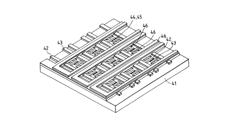
18, 19, 20, and 21. In these drawings, the numeral 41
denotes an insulating substrate; 42 and 43,
electrodes; 45, an electron-emitting region; 44, an
electroconductive film for obtaining sufficient
electric contact between the electrode and the
electron-emitting region; and 46, a modulation means.
In the apparatuses shown in Figs. 18, 19, and 20,
linear electron-emitting devices having a plurality of
electron-emitting regions are juxtaposed on the
substrate, and a plurality of ~rid electrodes
(modulation electrodes) 46 are placed in an XY matrix
with the linear electron-emitting devices. The grid
electrodes are placed above the electron-emitting face
of the electron-emitting device in Fig. 18; juxtaposed
on the same substrate plane as the electron-emitting
devices in Fig. 19; and laminated on the electron-
emitting devices by the aid of the substrate in Fig.
20. In the embodiment shown in Fig. 21, a plurality
of electron-emitting devices having each a single
~ 28 - 2~ 2
i electron-emitting portion are arranged in matrix, and
each element is connected to a signal wiring electrode
50 and a scanning wiring electrode 51 as shown in the
drawing. This construction is called a simple matrix
construction, in which the signal wiring electrodes 50
and the scanning wiring electrodes 51 serves as the
modulation means. The electron beam-generating
apparatuses exemplified above are driven as below. To
drive the apparatus illustrated in Fig. 18, 19, or 20,
pulsing voltage of 10 to 35 V is applied to the
electrodes 42 and 43 of one line of the linear
electron-emitting devices to cause emission of
electron beams from a plurality of the electron-
emitting portions. The emitted electron beams are
turned on and off by application of voltage of from 50
V to -70 V to the grid electrodes 46 in correspondence
with information signals to obtain electron emission
corresponding the information signals for the one
line. Such operation is conducted sequentially for
the adjacent lines of the linear electron-emitting
devices to obtain electron beam emission for one
picture image. To drive the apparatus illustrated in
Fig. 21, pulsing voltage is applied with the scanning
wiring electrode 51 to the plurality of the electron-
emitting devices on one line, and subsequently pulsingvoltage is applied to the signal wiring electrodes 50
- 29 - 2~ 92
l in correspondence with information signals to obtain
electron emission corresponding to information signal
for one line. Such operation is conducted
sequentially for adjacent lines to obtain electron
beam emission for one picture image.
Several examples are described above. The
electron beam-~enerating apparatus of the present
invention is advantageous in that the ineffective
current in the whole apparatus is extremely week,
electron-emitting characteristics such as electron
emission efficiency and electron emission stability
are excellent, and power consumption is low.
An image-forming apparatus of the present
invention is explained below. The image-forming
apparatus of the present invention has a constitution
such that an image-forming member is placed on the
electron beam emission side of the aforementioned
electron beam-generating apparatus. The image-forming
member is constituted of a material which causes light
emission, color change, electrification, denaturing,
etc. on collision of electrons, such as a light-
emitting material like a fluorescent material, and a
resist material. Fig. 22 illustrates one embodiment
of an image-forming apparatus of the present
invention. The apparatus of Fig. 22 comprises a rear
plate 52 (which may serve also as the aforementioned
30- 2~ 9~
1 insulating substrate 41), modulation means 4~ (which
are shown in a form of grid electrodes of Fig. 18, but
may be the grid electrodes of Fig. 19 or Fig. 20, or
the modulation means of Fig. 21), electrodes 42 and
43, electron-emitting regions 45, electroconductive
films 44 for obtaining sufficient electric contact
between the electrodes and the electron-emitting
regions, a face plate 58, a glass plate 57, a
transparent electrode 55, and a fluorescent material
56. To drive the image-forming apparatus of the
present invention, voltage of from 0.5 KV to 10 KV is
applied to the image-forming member (transparent
electrode 55 in Fig. 22), and then the apparatus is
driven in the same manner as driving of the above-
described electron beam-generating apparatus, thus an
image corresponding to information signals being
obtained on the image-forming member (fluorescent
image in Fig. 22). In the case where the image-
forming member is made of a light-emitting material
such as a fluorescent material, a full-color image
display can be obtained by using three light~emitting
materials of three primary colors of red, green, and
b].ue for one picture element. The electron beam-
generating apparatus and the image-forming apparatus
described above are usually driven at a vacuum of 10 4
to 10 9 torr.
-
: '.; ' : '
- 31 - 2~ 2
l The image-forming apparatus of the present
invention includes the embodiment shown in Fig. 28 and
Fig. 29. In the image forming apparatus shown by Fig.
28, a supporting member for supporting the atmospheric
pressure is provided between the face plate 58 and the
rear plate 52 in the image-forming apparatus of Fig.
23, Fig. 24, or Fig. 25. Fig. 28 illustrates
schematically the construction of an image-forming
member of the present invention. Fig. 29 is a
sectional view of the image-forming apparatus viewed
at around the atmospheric pressure-supporting member
of the image-forming apparatus shown in Fig 28. In
Fig. 28, the numeral 95 denotes an atmospheric
pressure-supporting member; 96, a supporting frame;
and 97, a luminescent spot of the fluorescent
substance. An envelop of the image-forming apparatus
is constructed of a face plate 58, a rear plate 52,
and a supporting frame 96. The internal pressure is
kept at a vacuum of 10 4 to 10 9 torr.
In an image-forming apparatus having no
atmospheric pressure-supporting member, the larger the
picture to be formed, the higher is the total
atmospheric pressure given to the face plate 58 and
the rear plate 52, and to support the increased
pressure, the face plate 58 and the rear plate 52 have
to be made thick, which inevitably increases the
- 32 - 2~
l weight of the apparatus. To avoid this disadvantage,
an atmospheric pressure-supporting member is provided
desirably. The atmospheric pressure-supporting
members 95 are placed usually at intervals of from 1
S mm to 100 mm between the picture elements so that
image defect may be avoided. The material of the
atmospheric pressure-supporting member 95 is an
insulating material such as glass.
When the image-forming apparatus having an
atmospheric supporting member 95 as shown in Fig. 28
and Fig. 29 is driven, the supporting member is liable
to be electrically charged by unexpected collision of
electron beam or ions against the supporting member 95
since the supporting member 95 is electrically
floating. This electric charging bends the locus of
the electron beam and changes the amount of the
electron beam colliding to the fluorescent material,
causing irregularity of luminance and color. It was
found by the present inventors that the disadvantage
caused by the electric charging of the supporting
member relates to driving voltage of the electron-
emitting device. If the ineffective current of the
electron-emitting device is large, the voltage applied
to the device is hiyh, and the supporting member 95
becomes liable to be charged. Accordingly, in the
present invention, use of an electron-emitting device
2 ~ 2
l causing weak ineffective current ma~es it possible to
obtain image-forming apparatus with large picture area
and light weight.
The image-forming apparatus of the present
invention includes the embodiments shown in Fig. 26
and Fig. 27, which are examples of optical printers
employing as the light source the image-forming
apparatus illustrated in Fig. 22. In Fig. 26, the
numeral 62 denotes the light source; 65 a drum; 63, a
delivery roller; and 64, a heat-sensitive or light-
sensitive sheet. The optical printer records image on
a recording medium by driving the light source as
described above (as driving of the image-forming
apparatus of Fig. 22) to emit light in correspondence
with information signals onto the recording medium 64
with scanning of the recording medium 64 supported by
a support 65 or 63, or the light source 62. Fig. 27
illustrates another embodiment of the optical printer.
The numeral 71 denotes a light source; 72, a drum-
shaped recording medium; 77, a developer; 75, a staticeliminator; 74, a cleaner; 73, an electric charger;
and 76, an image-transfer medium. This optical
printer records an image by electrical'y charging the
recording medium 72 with an electric charger 73,
projecting light beam emitted from the light source 71
in a manner as above (driving method of the image-
~ 34 - 2~ 2
l forming apparatus of Fig. 22) to the recording medium
72 to eliminate electric charge from the illuminated
area, adhering a toner on the non-illuminated area by
means of a developer 77, and transferring the toner
onto the image-transfer medium 76 by eliminating the
electric charge at the position of the static
eliminator 75.
The image-forming apparatus of the present
invention as described above is capable of forming
image with high contrast and sharpness with less
consumption of electric power. In particular, the
image-forming apparatus utilizing luminescent image
gives extremely small variation or flickering of the
luminance.
The present invention is described in more
detail below by reference to Examples.
Example 1
Electron-emitting devices of the type shown in
Figs. 1 to 3 were prepared. The procedure of the
preparation is described below by reference to Fig.
11 .
(1) A quartz substrate as the insulating
substrate 21 was cleaned sufficiently with an organic
solvent, and on the face of the substrate 21,
electrodes 22 and 23 were formed (see Fig. llA).
Metallic nickel was used as the material for the
- 35 ~ 2~ 2
l electrodes. The gap G between the two electrodes was
3 ,um, the length of the electrodes was 500 ~m, and the
thickness thereof was 1000 A.
(2) Organic palladium (CCP-4260, made by Okuno
Seiyaku K.K.) was applied thereon, and the applied
matter was heat-treated at 300~C to form a fine
particle film 24 composed of palladium oxide (PdO)
~average particle diameter: 20 A). The fine particle
film 24 had a length of 300 ,um and was placed around
the midpoint between the electrodes 22, 23 (Fig. llB).
(3) Then, as shown in Fig. llC, an electron-
emitting region 25 was formed by forming treatment:
that is, electric current is made to flow through the
fine particle film 24 by application of voltage
between the electrode 22 and the electrode 23. The
wave form of the applied voltage in the forming
treatment is shown in Fig. 12.
In Fig. 12, the pulse width Tl was 1.0
millisecond, and the pulse interval T2 was 10
milliseconds in this Example. The forming treatment
was conducted at the forming voltage as shown below.
under a vacuum environment of about 1 x 10 6 torr.
The electron-emitting region 25 was formed between the
fine palladium oxide film 4, and was composed of fine
palladium particles 6 as shown in Fig. 3. The fine
particles 6 had an average diameter of 10 A.
- 36 - 2 ~ 2
l Three devices of different areal occupation
ratio of the fine particles 6 were prepared by
changing the amount of the coating of the organic
palladium to change a sheet resistance of the fine
particle film 24 in the step (2) and changing the
forming voltage in the step (3).
1) Sheet resistance: 8 x 10 Q/square
Forming voltage: 4 V:
Areal occupation ratio of fine particles: 75 %
2) Sheet resistance: 3 x 10⁴ ~/square
Forming voltage: 7 V:
Areal occupation ratio of fine particles: 50 %
3) Sheet resistance: 5 x 10³ Q/square
Forming voltage: 13 V:
15 Areal occupation ratio of fine particles: 20 %
The devices were tested for electron emission
characteristics by means of the evaluation apparatus
illustrated in Fig. 16 under a vacuum of 1 x 10 7
torr. The results are shown in Table 1.
(Measurement method)
Fig. 16 illustrates schematically the
construction of the measuring apparatus. The
measuring apparatus comprises an insulating substrate
21, electrodes 22 and 23, an electron-emitting region
25, electroconductive films 24 for obtaining electric
contact, a power source 31 for applying voltage to the
- 37 -
2Q~92
l device, an ammeter 30 for measuring the device current
(If), an anode electrode 34 for measuring emission
current (Ie) emitted from the device, a high-voltage
power source 33 for applying voltage to the anode
electrode 34, and an ammeter 32 for measuring the
emission current. The aforementioned device current
means the current measured by the ammeter 30, and the
emission current means the current measured by the
ammeter 32. The device current and the emission
current of the electron-emitting device are measured
by connecting the power source 31 and the ammeter 30
to the electrodes 22 and 23, and placing, above the
electron-emitting device, the anode electrode 34
connected to the power source 33 and the ammeter 32
under a vacuum of 1 x 10 torr. From the results of
the measurement as shown in Fig. 6, the ineffective
current is calculated as below:
ineffective current = (Ix/If') x 100 (%)
where If' is the device current at a drive voltage Vd,
and Ix is the extrapolated value, at the drive voltage
Vd, of the straight line through the point of the
device current at the device voltage of zero and the
point of the device current at the device voltage Ve
where the device begins electron emission.
Example 2
Electron-emitting devices were prepared by the
- 38 -
2 ~ 2
l procedure below.
(1) A pair of electrodes were formed on an
insulating substrate in the same manner as in step (1)
in Example 1.
(2) A fine particle film 24 was formed in the
same manner as in step (2) in Example 1 (Fig. llB).
The resulting fine particle film was heated in a
reducing atmosphere (a mixture of hydrogen gas and
nitrogen gas) at 350~C, and then in the air at 350~C.
Thereby, the fine palladium oxide particles of 70 A in
diameter grew to have a diameter of 500 A. As the
results, the resulting fine palladium oxide film 24
was composed of particles larger in diameter than the
particles of Example 1. The sheet resistance of the
fine particle film 24 was 2 x 10⁴ Q/cm2.
(3) The fine palladium oxide film 24 prepared
in the above step (2) was subjected to the forming
treatment with the voltage wave form as shown in Fig.
13. In this Example, the pulse width T1 was 10
milliseconds, and the pulse interval T2 was 100
milliseconds.
Two kinds of devices were prepared by changing
the voltage in the forming treatment.
1) Forming voltage 6 V:
Average diameter of fine particles 6: 40 A
Areal occupation ratio of fine particles 6: 60 %
2~ 2
l 2) Forming voltage 13 V:
Average diameter of fine particles 6: 300 A
Areal occupation ratio of fine particles 6: 35 %
The devices were evaluated in the same manner
as in Example 1. The results are shown in Table 1.
Example 3
An electron-emitting device was prepared in
the same manner as in Example 2 except that the sheet
resistance of the fine particle film 24 was 5 x 10⁵
Q/square and the forming voltage was 4 V. In the
resulting device, the areal occupation ratio of the
fine particles 6 was 50 %, and the average particle
diameter of the fine particles 6 was 5 A. The
electron-emitting device exhibited approximately the
same effect as the ones in Example 2 (ineffective
current being not more than 1 %).
Example 4
Electron-emitting devices were prepared as
below.
(1) On an insulating substrate 21, electrodes
22 and 23 were formed with the electrode gap G of 1 ,um
(Fig. llA) in the same manner as in Example 1.
(2) A fine particle film 24 was formed
comprising fine palladium oxide particles (PdO,
particle diameter: 20 to 80 A, Fig. llB) in the same
manner as in Example 1. This fine particle film was
:
2~ 2
l heated in a reducing atmosphere (a gas mixture of
hydrogen and nitrogen) at about 200~C to give a fine
palladium (Pd) particle film (particle diameter: 15 to
60 A). The length of the fine particle film was 300
,um.
(3) An electron-emitting region 25 was formed
by application of voltage between the electrode 22 and
the electrode 23 for forming treatment of the fine
particle film 24. The forming treatment was conducted
with the voltage wave form shown in Fig. 12. The
pulse width T1 was 10 microseconds, and the pulse
interval T2 was 500 microseconds. The forming
treatment was conducted in a vacuum of about 1 x 10 6
torr.
Three kinds of devices were prepared by
changing the amount of the coating of the organic
palladium to change the sheet resistance of the fine
particle film 24 and by changing the forming voltage
as below:
1) Sheet resistance: 1 x 10⁵ Q/square
Forming voltage: 3.5 V
Average gap between particles: 12 A
Average particle diameter: 30 A
2) Sheet resistance: 5 x 10⁴ Q/square
Forming voltage: 6.0 V
Average gap between particles: 20 A
- 41 - ~ ~8 ~ ~ 2
l Average particle diameter: 35 A
3) Sheet resistance: 3 x 10⁴ Q~square
Forming voltage: 14 V
Average gap between particles: 50 A
Average particle diameter: 40 A
The devices were evaluated in the same manner
as in Example 1. The results are shown in Table 2.
Example 5
An electron-emitting device was prepared in
the same manner as in Example 4 except that the sheet
resistance of the fine particle film 24 was 1 x 10⁵
Q/square and the forming voltage was 4 V. In the
resulting device, the average particle gap was 5 A,
and the average particle diameter was 50 A. The
electron-emitting device exhibited approximately the
same effect as the ones in Example 4 (ineffective
current being not more than 3 %).
Example 6
An electron-emitting device was prepared in
the same manner as in Example 4 except that the sheet
resistance of the fine particle film 24 was 5 x 10³
Q/square and the forming voltage was 14 V. In the
resulting device, the average particle gap was 100 A,
and the average particle diameter was 50 A. The
electron-emitting device exhibited approximately the
same effect as the ones in Example 4 (ineffective
- 42 - 2 ~ 2
l current being not more than 1 %).
Example 7
Electron~emitting devices were prepared as
below.
(1) On an insulating substrate 21, electrodes
22 and 23 were formed in the same manner as in the
step (1) in Example 4 (Fig. llA).
(2) A fine particle film 24 of palladium (Pd)
(particle diameter: 60 to 500 A) was formed in the
same manner as in the step (2) in Example 4 except
that the temperature of heating in the reducing
atmosphere was 370~C (Fig. llB).
(3) An electron-emitting region 25 as shown in
Fig. llC was formed by forming treatment. The forming
treatment was conducted with the voltage wave form
shown in Fig. 13, the pulse width T1 of 50 -~--
microseconds, and the pulse interval T2 ~f 500
microseconds.
Two kinds of devices were prepared by changing
the amount of coating to change the sheet resistance
of the fine particle film 24, and by changing the
forming voltage.
1) Sheet resistance: 5 x 10⁴ Q/square
Forming voltage: 4.0 V
Average gap between particles: 20 A
Average particle diameter: 40 A
- 43 -
2~0~
l 2) Sheet resistance: ~ x 103 Q/square
Forming voltage: 12 V
Average gap between particles: 35 A
Average particle diameter: 300 A
The devices were evaluated in the same manner
as in Example 1. The results are shown in Table 2.
Example 8
An electron-emitting device was prepared in
the same manner as in Example 7 except that the sheet
resistance of the fine particle film 24 was 3 x 10⁵
Q/square and the forming voltage was 4 V. In the
resulting device, the average particle gap was 30 A,
and the average particle diameter was 5 A. The
electron-emitting device exhibited approximately the
same effect as the ones in Example 7 (ineffective
current being not more than 1.0 %).
Example 9
Electron-emitting devices were prepared as
below. The procedures explained by reference to Fig.
14.
The steps of Figs. 14A to 14C were practiced
in the same manner as in the steps (1) to (3) in
Example 1 except that the forming treatment was
conducted with the voltage wave form as shown in Fig.
12 at the forming voltage of 8 V, the pulse width of
T1 of 1 millisecond, and the pulse interval T2 of 10
2~Q~2
milliseconds.
(4) As shown in Fig. 14D, organic palladium
(CCP-4260, made by Okuno Seiyaku K.K.) was applied at
a desired position by dipping. The applied matter was
heat treated at 320~C to form a fine particle film 24-
b composed of fine particle of palladium oxide (PdO)
on the electron-emitting region 25-a.
(5) Then as shown in Fig. 14E, the electron-
emitting region 25-b was formed by forming treatment
conducted in the same manner as before. In this
treatment, the electron-emitting region 25-b was
formed nearly the same position as the initially
formed electron-emitting region 25-a. Repetition of
the steps of (4) and (5) of this Example enables the
control of the gaps of fine palladium particles 6.
Thereby, three kinds of devices were prepared as
below.
1) The steps (4) and (5) were conducted three
times:
Average gap of fine particles: 12 A
Average diameter of fine particles: 35 A
Areal occupation ratio of fine particles: 65 %
2) The steps (4) and (5) were conducted twice:
Average gap of fine particles: 20 A
Average diameter of fine particles: 30 A
Areal occupation ratio of fine particles: 50 %
~ 45 ~ ~ ~0~92
L 3) The steps (4) and (5) were conducted once:
Average gap of fine particles: 50 A
Average diameter of fine particles: 25 A
Areal occupation ratio of fine particles: 30 %
The devices were evaluated in the same manner
as in Example 1. The results are shown in Table 3.
Example 10
An electron-emitting device was prepared in
the same manner as in Example 9 except that the steps
(4) and (5) were conducted four times. In the
resulting electron-emitting device, the areal
occupation ratio of the of the fine particles in the
electron-emitting region was 75 %, the average
particle diameter of the fine particles was 35 A, and
the average gap of the fine particles was 5 A. The
device was evaluated in the same manner as in Example
9. The effect was nearl~ the same as that of Example
9 (ineffective current: not more than 2.0 %).
Example 11
An electron-emitting device was prepared in
the same manner as in Example 9 except that in the
step (4) the forming voltage was 12 V. In the
resulting electron-emitting device, the areal
occupation ratio of the fine particles in the electron-
emitting region was 20 %, the average particle
diameter of the fine particles was 25 A, and the
- 46 - 20~0~
l average gap of the fine particles was 100 A . The
device was evaluated in the same manner as in Example
9. The effect was nearly the same as that of Example
9 (ineffective current: not more than 0.2 %).
Example 12
An electron-emitting device was prepared in
the same manner as in Example 9 except that in the
step (4) the forming voltage was 12 V, and the steps
(4) and (5) were conducted twice. In the resulting
electron-emitting device, the areal occupation ratio
of the of the fine particles in the electron-emitting
region was 50 %, the average particle diameter of the
fine particles was 300 A, and the average gap of the
fine particles was 30 A .
The device was evaluated in the same manner as
in Example 9. The effect was nearly the same as that
of Example 9 (ineffective current: not more than 1.0
%) .
Example 13
Electron-emitting devices were prepared as
below. The procedures explained by reference to Fig.
15.
(1) and (2) The steps of Figs. 15A and 15B
were practiced in the same manner as in the steps (1)
and (2) in Example 1.
(3) ~ part of the fine palladium oxide
- 47 - 2~ 2
l particle film 24 is irradiated with electron beam to
reduce the palladium oxide to form a fine particle
film 26 composed of fine palladium particles (particle
diameter: 15 to 60 A) (Fig. 15C). The electron beam
5 irradiation was practiced under the conditions of an
electric current of 30 nA, an accelerating voltage of
30 kV, and a vacuum of 1 x 10 torr. The fine
palladium particle film 26 was formed in a width of
1000 A around the center of the fine palladium oxide
film 24.
(4) Then as shown in Fig. 15D, the electron-
emitting region 25 was formed by forming treatment.
The forming treatmen~ was practiced by applying
voltage between the electrode 22 and the electrode 23
lS in the voltage wave form shown in Fig. 12 in the pulse
width T1 of 70 microseconds, and the pulse interval T2
of 500 microseconds. Three kinds of devices were
prepared by changing the forming voltage as below.
1) Forming voltage: 3.5 V:
Average gap of fine particles: 12 A
Average diameter of fine particles: 25 A
Areal occupation ratio of fine particles: 65 %
2) Forming voltage: 6.0 V:
Average gap of fine particles: 20 A
~5 Average diameter of fine particles: 28 A
Areal occupation ratio of fine particles: 50 %
- 48 - 2~0~2
l 3~ Forming voltage: 14 V:
Average gap of fine particles: 50 A
Average diameter of fine particles: 35 A
Areal occupation ratio of fine particles: 35 %
The devices were evaluated in the same manner
as in Example 1. The results are shown in Table 3.
1~ /
;
~ 49 ~ 2~0~2
l Example 14
An electron ray-generating apparatuses were
prepared by arranging in a line a plurality of the
electron-emitting devices prepared in Examples 1 - 13
as shown in Fig. 17. The apparatus comprises an
insulating substrate ~a rear plate) 41, wiring
electrodes 42 and 43, low-resistance portions 44
having low electric resistance, electron-emitting
regions 45, modulation means (grid electrodes) G1 to
GL (46), and electron-passing holes 47. The spacing
between the insulating substrate 41 and the modulation
means 46 was adjusted to 10 ~um. The electron beam-
generating apparatus was driven as described below.
The apparatus was placed in the vacuum of 10 6 torr.
Driving voltage (device voltage in Examples 1 - 13)
was applied between the wiring electrodes Then
voltage of 30 V was applied to the modulation means in
accordance with information signals. Thereby,
electron beams were emitted from the plurality of the
regions 45 in accordance with the information signals.
The electron beam-generating apparatuses of
this Example consumed less electric power because the
ineffective current in the device current was
extremely low (2 % or less). Therefore, the electron-
emitting devices could be arranged in fine pitch inthe apparatuses. Further, since the current flowing
- 50 - 2~ 09 2
l through the electrodes 42 and 43 was weak, the voltage
drop between the electrodes 42 and 43 was small, and
the oluantities of the electron beams (or emission
current) emitted from the elements were uniform.
Therefore, many elements could be arranged between the
electrodes 42 and 43.
From among the above electron-emitting devices
in this Example, more effective were those of Example
1 (1) and (2), Example 2 (1), Example 3, Example 4
(1), (2), and (3), Example 5, Example 7 (1), Example
8, and in particular, Example 9 (1), (2), and (3), and
Example 12 (1), (2), and (3) in that the driving
voltage of the electron-emitting device was low, the
emission current was strong, and variation of the
emission current between the devices was small.
Example 15
Electron beam-generating apparatus were
prepared by arranging in lines a plurality of linear
electron-emitting device groups comprising the
electron-emitting devices of Examples 1 - 13, as shown
in Fig. 18. The spacing between the insulating
substrate 41 and the modulation means 47 was adjusted
to lO ,um, and the interval between the linear electron-
emitting device groups was adjusted to 1 mm. The
electron beam-generating apparatus was driven as
described below. The apparatus was placed in the
- 51 -
1 vacuum of 10 torr. The driving voltage (device
voltage in Examples 1 - 13) was applied between the
wiring electrodes 42 and 43. Then voltage was applied
to the modulation means 46 in accordance with
information signals: the electron beam beiny
controlled to be off at 0 V or lower, being controlled
to be on at +30 V or higher, and to vary continuously
between 30 V and 0 V. Consequently, electron beams
were emitted from a plurality of electron-emitting
region 45 in a line between the wiring electrodes 42
and 43 in accordance with the one line of information.
This operation was conducted sequentially for adjacent
lines of the linear electron-emitting device group to
obtain electron emission for the entire information
signals.
In this Example also, the similar effects as
in Example 14 were confirmed.
Example 16
Electron beam-generating apparatuses were
prepared in the same manner as in Example 15 except
that the modulation means tgrid electrodes) 46 were
placed on the face of the insulating substrate 41.
The emission of electron beams could be made in
accordance with information signals by driving the
apparatus in a similar manner as in Example 15. In
the apparatuses of this Example, the electron beams
- 52 - 2Q~Q~
l could be controlled by the voltage applied to the
modulation means: to be off at -30 V or lower, to be
on at +20 V or higher, and to vary continuously
between -30 V and +20 V.
In this Example also, the similar effects as
in Example 14 were confirmed.
Example 17
An electron beam-generating apparatus was
prepared in the same manner as in Example 15 except
that the modulation means (grid electrodes) 46 were
placed on the face of the insulating substrate
opposite to the electron-emitting face of the linear
electron-emitting device groups. The emission of
electron could be made in accordance with information
signals by driving the apparatus in a similar manner
as in Example 15. In the apparatuses of this Example,
the electron beams could be controlled by the voltage
applied to the modulation means: to be off at -30 V or
lower, to be on at +20 V or higher, and to vary
continuously between -30 V and +20 V.
In this Example also, the similar effects as
in Example 14 were confirmed.
Example 18
The electron beam-generating apparatus of this
Example has the construction shown schematically in
Fig. 21. In this apparatus having a simple matrix
2 ~ 2
l construction, a plurality of electron-emitting devices
of any of Examples 1 to 13 are arranged in matrix, and
each device is connected to a signal wiring electrode
50 and a scanning wiring electrode 51.
The apparatus was driven as below. The device
voltage indicated in Examples 1 to 13 was applied to
each of the electron-emitting devices to cause
electron emission from the electron-emitting devices.
Firstly, pulsing voltage of 0 V or half the device
voltage was applied by the scanning wiring electrode
~ 51 to one line of a plurality of the electron-emitting
devices. Then another pulsing voltage of 0 V or half
the device voltage was applied to the signal wiring
electrode 50 in correspondence with information
signals to obtain the electron beam emission in
correspondence with the information signa~s for the
one line. Such operation was conducted sequentially
for adjacent lines to obtain electron beam emission
for one picture image.
In this Example also, the similar effects as
in Example 14 were confirmed.
Example 19
An image-forming apparatus as shown in Fig. 22
was prepared by use of the electron beam-generating
apparatus of Example 15. In Fig. 22, the numeral 58
denotes a face plate; 57, a glass plate; 55, a
- 54 - 2~0~
l transparent electrode; and 56, a fluorescent material.
The spacing between the face plate 58 and the rear
plate 52 was adjusted to be 3 mm.
The image-forming apparatus was driven in a
manner shown below. The panel vessel constructed from
the face plate 58 and the rear plate 52 was evacuated
to a vacuum of 10 6 torr; the voltage of the
fluorescent material face was set through the EV
terminal 59 at 5 KV to 10 K~; and pulsing voltage
(namely the device voltage indicated in Example 1 to
13) was applied to a pair of wiring electrodes 42 and
43. Then voltage was applied to the modulation means
through the wiring 54 to control the electron beam
emission to be on or off in accordance with
information signals: the electron beam being
controlled to be off at -30 V or lower, being
controlled to be on at 0 V or higher, and to vary
continuously between -30 V and 0 V, thus gradation
display being practicable.
The electron beams emitted through the
modulation means in accordance with the information
signals collided against the fluorescent material 56
to display one line of information of the information
signal. This operation was sequentially conducted to
obtain a display of entire picture. The image
displayed by the ima~e-forming apparatus of this
~ 55 ~ 2~ 2
l Example exhibited low irregularity in luminance, and
gave a sharp image with high contrast. The image-
forming apparatus having a well-known constitution of
a cathode beam tube gave a sharp color image with high
contrast with less irregularity of luminance by use of
a face plate employing color fluorescent materials of
R (red), G (green), and B (blue).
Example 20
An image-forming apparatus as shown in Fig. 23
was prepared by use of the electron beam-generating
apparatus of Example 16. The apparatus was driven to
display a luminescent image of the fluorescent
material in the same manner as in Example 19, except
that the voltage applied to the modulation means was -
40 V or lower to control the electron beam ~o be offand +10 V or higher to control the electron beam to be
on. In the voltage range between -40 V to ~10 V, the
quantity o:F the electron of the electron beam varies
continuously, thereby gradation of display being
practicable.
In this Example also, the same effects as in
Example 19 were confirmed.
Example 21
An image-forming apparatus as shown in Fig. 24
was prepared by use of the electron beam-generating
apparatus of Example 17. The apparatus was driven to
- 56 - 2 Q~ Q09 2
1 display a luminescent image of the fluorescent
ma~erial in the same manner as in Example 19, except
that the voltage applied to the modulation means was -
40 V or lower to control the electron beam to be off
and +lO V or higher to control the electron beam to be
on. In the voltage range between -40 V to ~10 V, the
quantity of the electron of the electron beam varies
continuously, thereby gradation of display heing
practicable.
In this Example also, the same effects as in
Example 19 were confirmed.
Example 22
An image-forming apparatus shown in Fig. 25
which is similar to the one of Example 19 was prepared
by use of the electron beam-generating apparatus of
Example 18. In Fig. 25, the numerals 51 and 52
respectively denote a wiring connected to the scanning
wiring electrode and a wiring connected to the signal
wiring electrode.
The image-forming apparatus was driven in a
manner shown below. The panel vessel constructed from
the face plate 58 and the rear plate 52 was evacuated
to a vacuum of 10 6 torr; the voltage o~ the
fluorescent material face was set through the EV
terminal 59 at 5 KV to 10 KV. Electron beams were
emitted from the electron-emitting devices on
- 57 - 2~
l application of the device voltage indicated in
Examples 1 to 13 to the electron-emitting devices.
Firstly, pulsing voltage of 0 V or half the device
voltage was applied by the scanning wiring electrode
51 to one line of a plurality of the electron-emitting
devices. Then another pulsing voltage of 0 V or half
the device voltage was applied to the signal wiring
electrode 50 in correspondence with information
signals to project the electron beam to the
fluorescent material 56 in correspondence with the
information signals for the one line. Such operation
was conducted sequentially for adjacent lines to
obtain display of one picture image.
In this Example also, the similar effects as
in Example 14 were confirmed.
Example 23
An image-forming apparatus shown in Fig. 28
was prepared by providing an atmospheric pressure-
supporting member 95 additionally in the image-forming
apparatus of Example 22. In this Example, the
apparatus was driven in the same manner as in Example
22, and nearly the same results were obtained,
Furthermore, the face plate and the rear plate could
be made thinner, whereby the weight of the image-
forming apparatus could be reduced, and the picturescreen could be enlarged.
- 58 -
2~0~2
Tabl e
Electron- Device Device Emission In- Voltage Electric
emitting voltage current current effectiv~application field
device current length strength
V mA ~A % A 107 V/cm
Example 1
(1) 16 2.2 2.0 2.0 50 3.2
Example 1
(2) 18 1.5 1.2 0.8 100 1.8
Example 1
(3) 30 0.18 0.2 0.6 300 1.0
Example 2
5(1) 18 ]--3 1.3 0.7 100 1.8
Example 2
(2) :L8 0.8 0.8 0.7 100 1.8
~ 59 ~ 2~8~9~
Table 2
Electron- Device Device Emiss.ionIn- Voltage Electric
emitting voltage current current effectiveapplication field
device icurrent length strength
V mA ~A % A lO V/cm
Example 4
(l) 13 3.0 1.5 1.230 4.3
Example 4
(2) 14.5 2.0 l.S 0.740 3.6
Example 4
(3) 16 0.1 0.2 0.3120 1.3
Example 7
5(1) 14.5 2.0 1.6 0.740 3.6
Example 7
(2) 14.5 0.8 0.6 0.740 3.6
- 60- 2Q~0~2
Table 3
Electron- Device Device EmissionIn- Voltage Electric
emitting voltage current current effectiv~ application field
device ' current length strength
V mA ~A ~ A 10 V/cm
Example 9
(1) 13.5 3.5 2.8 1.0 30 4.3
Example 9
(2) 14 2.5 2.5 0.5 40 3.6
Example 9
(3) 16 0.3 0.5 0.3120 1.3
Example 13
5(1) 13.5 3.5 3.0 0.9 30 4.3
Example 13
(2) 14 2.5 2.7 0.4 40 3.6
Example 13
20(3) 16 0.3 0.6 0.2120 1.3