Note: Descriptions are shown in the official language in which they were submitted.
~08~46~
S~LY a~r OF TÆ ~:DIT C~RD TYPE
T~ i~tian relates to elec~ical en~rgy storing
devices and mo~:e speci ficall~ bo energy st~ring far syst~ns
canprisir~g mic~el~ic inte~rate~ cir~its with ~.
~ resently, there an3 thcee main types of ~lec~ic
5 supply sa~es ~or microelec~ic cira~its (a chip or a onplex
elecl~ nic sys~ m having a d~ ~ fw~cticn):
1) th~ 110 or 220 V malns from which, afber vDltage
lowering by a transformer, rectifying, filtering and ccntxolling
or use of swi ~ devices, a D.C. v~l~age:~usually from 5 to 15
volts) is prcvided to the microelectronic circui~;
2) the batbery which is a self-ccntaind supply sourQe
for an electrcnic dbvioe;
3) the rechargeable batbery or accumulabcr, whic:~ was
usually a lead acc~la~ and ~ich is p~tly, gener~ly, in
15 ff e field of electronic circuit ~eed~ng, a ca~ Lum-nickel aca~-
lata~.
Ihe mains p~3sents of course the advantage of being a
lar~ en~rgy ~urce (in as much as the A.C. mains a~ 110 or 220 V
is reliable) but has ~ maj~r draw~cs, that is, being
20 ~e, weigh~, nDisy~ subject ~ parasibes, ar~ not
~le.
~ e non-recba ~ l~ batte~y has t ~ draw~a~ of a
limibed li~etime, a ra ~ poor reli~bility in an hcætile e~wi-
rcnment, ~nd a high cost.
-.
.
- ' ' ' ~ '
208B~6~
Ih~efc~re, ~e ~xresent tr~ is ~o use r~le
aaa~la~s. Self ccntair~d like a batt~y, an a~ator
sc)lve~ ~e E~blem of ~e llfetime due to ~e po~sibility of
~ging, ~ ~ of ~cges va~ a~d~
5 el}~nical nature of ff2e a~a~., Ihe p~blffn of
reliability is h~ver nc~t solved. Additi~ally, r~ar~3~
~its for ~ur~le a~mulabcsrs ~e ge~2erally ~latively
ccmplex and g~rate an el~tic n~iæ. Ad~i ticnally, if
10 cu~ ar~ tak~ an irflportant surfæ on a print~3d ci~t
~ard prwided in ~he syst~n.
An cbj~t of ff~ ir~enti~ is to provid~3 ~ an aQwru-
latar syst~ with all its r~char~ and test elemerlts havir~ t~
form of a ælf{~c~tair~d portable: oanpa~t.
A more sp~dfic ab~ect of the ir~entiQn is to lmplement
~SU~I a self-oontained oompcnent having the usual cr3~Lt card
format ( thin rec~u~ar card of about 85 x 54 cm).
For att ~ thcse cb~ects, the invention prc~i~C~ for
a self-oontained portable el ~ ic componEnt having a credit
20 card fonTat c~rising at least ~ aoc~lator }na~e of a pile of
sheets or planar layar~s, the surfaoe of which is s~tially
equal to the surface of the ~it card, at least a charglny
circ~it and state in~icatc~s oontc~lled bs~ a microc~ntroller
associated to means for measurin~ at short and regularly spaced
25 time intervals the c~rrent in the accumulator and msans ~or
calculating, storing, and summiny the charye variations.
Af~ordi~ t~ an ~t of the inventicn, the stat~
:Lndicators ocsnprise an indicator of the residual n~r o
po~sible ~arges associated to t~e mean~s for ~ the oh~ge
variatians durir~g the diæha~e p~as~.
1~ to an ~i~t of the im7ention, ~e state
ir~ic~ators compriæ a ~ar~e ratio indicator ass0ciabed t:o the
means for s~n~ni~ tl~e ~ e variat:icns durin~ t~e ~harge and
di~char~ phases.
hx~ to an 0b~ent of t~e i~ti~, the state
indicat~rs c~riæ an instarl~ c~lc~ indicabo~
~0~5
associat~3d with n~s f~r m3asur~ t~e v~ltage va~iatian at
arly spaf~3d time in ~ . ...
Preferentially, ~e a~latar i~ c~ accmulat~r wi~
a poly~rer solid state electrolyte made of th:Lrl 1 3yers h~vir~ a
5 thickness of 1 to 500 micr~rete:rs havir~ auboclis~ar~e char~-
Aaa~rding to an ~in~t of t~ irnJenti~, c~e of ~æ~nal surfc~s of ~e ca~t ca~riæs a soL3r cell arra~.
I'his ext~nal fc~e, or ~ o~r ~e, canprises c~ ~lec~ode area
10 for charyin~, us~ and ex~anging data with exte~n~ devices,
this elec~ area 2 aving the stc~ard format of cr~dit cards
el~s.
~ cdis~ to an ~ lin ~ t of ~ e i~ention, this
oomponent comprises, above the sheet pile oonstituting the accu-
mulator, at le2st one printed circuit board, one at least of
those boards being prcvided with openings wherein are dispo6ed
some at least of the electronic circuit elemenbs nel essRry to the
operation of the component and the upper board comprising aper-
tures wherein ~re disposed the stabe indicabors.
Acicrd1ng b~ an enb3diment of the invention, this
compcnent oomprise~ an encoding keybcard.
Those ob~ects, features and advantages and others of
the i tion will be explained in greater detail in the follo-
wing description of preerred embodlments, in relation with the
attached drawings wherein:
Figune 1 il.lustrates various elements 1ncnrporated in
a self-oontained compcnent acm rdlng to the invention;
Figu~e 2.1 is a schematic fnont view of an accumulabor
~Pll aicordbng to the ~ tion and figure 2.2 is a section view
of the cell;
Figure 3 is a schematic cross section of an arrangemRn~
o~ elements ~ ituting an embodlnent of the invention; and
Figure 4.1 is a schematic front vlew of ~he mtlucbul3
of figure 3; and figure 4.2 is a view of the other ~ æ of the
s~r~cblre o~ figune 3.
.
- 2 ~ 6 ~
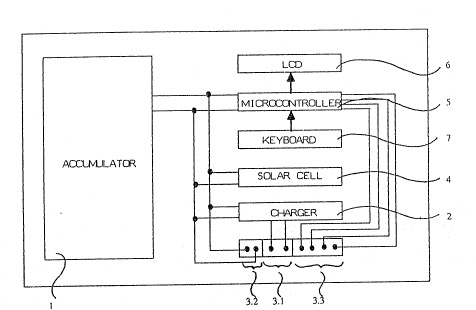
~ris~ for its c~ging ~ its t~stir~ a ~et oE el~snts of
an a~latc~r æt 1, a ~arging c~it 2, a ~cr~c~r 3 havir~
5 c~arging ~min~s 3 .1, utillzation ~ls 3 . 2 and dlata
ex~a~e termi~s 3.3., a solar c~ll 4, being a~ ~ar~ing
n~s, a micma~troller 5 associa~d wi~ display cir~uits 5 f~
prwiding varia3s infnaticns cn t~3 state of a~mulat~es 1,
ar~ an opticnal k~o~ 7 fo~ data input.
AS ir~c~ted a~, ~se el~nts usually exist in t~
form of various ccmp~ts ~oed at varials positia~s of a
syst~n, p~;sibly cn the sa~ E~rinted Gi:rwit board.
The ob~ect of the pres ~t i~venticn is, OQ the c ~
hand, to assemble those elements ln the form of a single po¢table
ob~ect having a credit card format, on the other hand bo prov.tde
for sp3~tfic modes of testing and dtsplaying the state of accumu-
lator 1 w~tle using co~mon means for the implementation of the
various tests, whereby the system is si~plified and less cumber-
saT e.
In this ~ , the inNention uses, as an energy
scurc2, an accumwlabor having a negligeable autodischarge formed
fro~ sheets or layers.
A nan limdtatlve example of such an accumulator is
shown in figures 2.1 ~nd 2.2. It comprises, on a metallic anode
11, whlch is a curr~nt oollecbor, a set 12 oomprising a composite
anode layer 13, mainly comprlsed of lithium, a polymer electro-
lyte 14 and a cathkde 15 made of a plastic oomposite material.
Conwentionally, each of the layers 11, 13, 14 and 15
has a thickness ~n the range of 50 ~m. AooDr ~ ly, tha whole
thi ~ of a cell, such as the o~e of figure 2.2 may be of
abGut 0,2 mm.
m e i~v~ntion uses such a layer set on substantially
all the available ~rrface of a structun~ of the credit card ~ype,
ccnNenticnally having lateIal dimensions of 8~ x 54 ~m, that is
abcut 40 cn~. With such a cell, one obtains a rated ene¢gy of
2~81D~5
volt. This cell has t~2e advan~age o~ })earin~ a}x~ut 100~) ~y~l s of
~arg~ afte~ a dee~ dis~ ins~ad of cnly 500 c~ycles f~r
la.3er ~ 0,01 96 p~r y~r at 25C instead of 25 % p~r ~nm ~ar
the ni~el~hTium. F~lr1~re, ff~is d~ioe nay ~rate in a
~ature range of -20 to +150C.
So, in a ~ular film of 8 J~ 5 (m, having a tllick-
ness of 0, 2 mm, cne cibtains a K>ltage of 3 v~lts a~ a rated
er~gy of 40 nAh. F~r cbtaining a 6 volt volty~e, a bloc:k asso
r; ating t~ el~rentary ~rially ~ cells is form~d. Five
parallel bloc}cs pr~vide a v~lta~e of 6 volts ~it~ a rat~d energy
of 200 IrAh.
Aaoardingly, ~ e inv~tian provides an accunulator
having a credit card format with a planar elec*rode str w bure of
ths typa sh~n in flgures 2.1 and 2.2.
An example of ~h an arranJCment is illustrated in
figure 3. The accumulator plates ll and 12 of flgure 2 are shcwn,
plabe ll averhanging with ~espect ~o plate 12 for farming an
ancde oGntaCt on its upper surfaoe. It is clear that a ~PU pile
can also be used. The la ~ are formed or assembled on a carrier
20 made of a plastic film fo ~ the lower surfaoe of the cell,
this film ha~lng apertures wherein solar cells 28 are placed.
A first printed circuit board 21 is used in particular
for establishing a oontact with anode ll. A second prinbed
Gircuit board 22 and a ~hird printed circult board 23 are also
shown.
In the figure, the prinb~d ci~ w it board 22 comprises
apertures 24-26. In those apertures are arrang3d int2grated
circuits or other ~ ectronic oomponents, ~or example, an integra-
ted cdrcuit camprising all the elements n~c~#:&Lry for charging
the accumulabor from t~e mains, the mic~ooGn~roller 5 ~f figure
1, etc.~ The surfaoes of the prinbed circuit 22 ccmpri æ means
for ocnn2cting the various elements and the accumulator elec-
trodes ll, 12.
.
.. -, ...... . . ' : ~
2~8D~
In a fi~st a~ of the prinbed cir~uit board 23 ar~
ex(::ha~ and, in varia~s aE~tur~ 29-32 ( rP,fer b~ ~igure 4 ),
displa~ devi~es. 1~ device is oo~ered wil~ a t~t plastic
film 35 ~ which appear ~e ~r eleG~od~ 33. In
a~ 29 a~ear tw:> ccntrol li~hts, f~r ~e s~la~ cell an~ ~e
~e ci~t. mrwgh ape;rt~ 30 32 app~ar far ~mple
c~:ystal liquid displays, r~vely for ~e char~e ratio, the
10 eKplain~ in deta:al h2reirlafter.
Ir~d, an aspect of the ~ian is tt~ pmvide for
~ e display of state infoImati~n fo~ E ~ vid:ing a really self-
oontained and reliable aocumulabor permanently providiny indica-
tions on its cwn state.
Generally, a ~ltage measure~ent acxcss an acc~Llabor
provides an i ~ ate me~surement of the charging state of this
aocumulator. This is dNe to the f3ct that the disc~r~e/chary0
curve is nok linear in the useful voltage range and, additional-
ly, depe~ds upon the load corr ctrd to th~ accumLlator.
ALoarding to th~e inwention, the ab~ve mentioned micro-
co~troller is used for takiny measLremrnts of the current Il
flowing through the accumulabor at times tl separated by regu-
lar time intarvals ~t. ~t is chosen small enough for ccnsidering
that the current is constant during a time inteIval ~t. Thus, ~he
charge v~riation o~ in the accwm~lator is:
~ t~
I being negative in case of discharge and positive in case of
charge. Knowing the maximum char~e ~ of the a~clmulator,
whlch is a characteristic data thereof, thLse charge variations
are summed ~n a regisber:
tI
At eveLy time, the charge stats ~ is cal llated:
/Q a x ] ~ in %-
. .
~ '~ , . ~ ...... .. .' . .
.. . . .
.
2 ~
e aa~rrn~labar at~ a deep dis~har~, ane has:
rl = Q~
~ ~e a~lato~ i5 fully *~d, C~ has:
~Qi =
rl - 100 %,
the r~gist~r is reset.
Ihis simple operaticm is easily caIried out bs! a micnD
~ roller E~ widec~ wiff~ calallati~, stc~rir~, analogic input-
a~tput, ar~ display cx~t~ Teans. Additicnally, wh ~ themeasuLed charge state gets lower than a predetermined threshDld,
the oontr~ller inhibits the output on the utilization circuit fQr
avDiding an exoessive discharge of the oantroller, which could
impalr this acsumulabor and for rnaintaining the operation of the
microoontrDller and its asso~iated r~3m~ries.
Mbas~D~nent of the in~an~s consumption is r~de in
a similar way by measuring at ~ach time interval ~t th~ vralue of
the volta~e across th3 accumulabor and by calculating the diffe-
rence ~ with } t bo the volta3e measured during the fo~mer
20 time int~:val. ~ value ~V/~t irxlicates tt~ ~ato~ fla~ o~
instanta~us ~su~tlal.
Aa~dir~ to an aspect of thle i~tion, t~e residual
lifeti~e of the accumulat~r is also calculabed. Indeed, an aocu-
mulator can be s ~ tted t~ a deb ~ number of charge and
discharge cycles. It has a lifetime of N ~ull cycles and a capa-
city e~l to Nx~ . Hbwever, in practioe, ~he me.sulenent .is
m~re ccmple~ due to the fact that it happens that the ~lat~
is charged while it is not yet fully discharged. There~ore, one
uses the aboNe mention2d neasureLent of the cha~e variation (~Q
= I~t) for m3asuring the charge rate. The total cha¢ge prcvided
~y ~e ~n~la~r sin~ it~; first ~ e is sk:~red in a r~gis-
me residual lifetime is ~ly e~cess~ ~:
- ~ /~, ~, Y
:
2~$~6~
T~3 displ~3y in the ab~ve mEntic~3d ap3rb~e 32 can b2
~r~latar.
q~ card e~dlng to ~ae invential c~riæs a c~w3c-
ll~L as ca~ti~ally us~i with c~lit cards ( ~nr 33 of
sl~s ~ reoeivin~ c~csr~ti~ cr~dit cards.
q~ i~ticn is liable of nE~ variant~s ~1 n~difica-
tions ~ich will a~ to ffY~se skill~d in t~ art, as r~gards
t~e select~an arxl the a~ar~t of ~e varials elements.
A coding l~e~oar~ 34 ( figures 3 and 4.1 ) ~xrwides a
~-trolled ac~ess to l~he souroe c~Rprised ~ the OEd a~ to an
In ~icular, those skilled in the art will be able b~
c~0~3e and program a microcontroller hav:Lng m~ry an~ display
contrt~l msar,s fa¢ satisfying the above mentic~ f~tions, fcr
exa~ls, the microcx ntroller ,upl~75328 ~C of Nippon ~:1ectric (~p.
P~ditia~ally, the ~t disclosed in nnecti~
with figure 3 ccnstitutes c~l~ an ~Tplary ~cli~t o ff-e
i~tial. Tho6e ~killed in t~e art will be able ~:> E~vide me~s
~ther than a pile of t~ree prin~d ci~wit ~s c~ associa-
tir~, ~d~ to a cLedit card f~rmat, vario~s ~ar~e and
m~s~t elemen~s with arl aoaDnulab~r oanprising a pile of
~ ets ~r planar lay ~ s.
Add~ticnally, t~ ao~lator and test ~elf~tain~d
a:~npc~t ~rdi~ to the .Lnventic~ has been abc~ve disalo6ed in
oonnecticn with an auto test use, ~hat is th~, test elements ar~,
used ~or testinç~ ff~e aa~la-tor of the cnp~ent itself.
qhis self contained cc~t, associat~3d with ~e
abc~ve m~ti~ed coding }~ can also be used as a o~npl~Tent
of a main energy sour~e, for:
- ætting it,
- ~ir~ its ~ge, ins~tane~s <~tia~
lifetime paramet~s,
..
-
. ~ . , .
~8~
- ~e~s~ it...
elec~ic o~ k~y.
, ' ,, ~ ,, ' '
.