Some of the information on this Web page has been provided by external sources. The Government of Canada is not responsible for the accuracy, reliability or currency of the information supplied by external sources. Users wishing to rely upon this information should consult directly with the source of the information. Content provided by external sources is not subject to official languages, privacy and accessibility requirements.
Any discrepancies in the text and image of the Claims and Abstract are due to differing posting times. Text of the Claims and Abstract are posted:
| (12) Patent Application: | (11) CA 2080479 |
|---|---|
| (54) English Title: | PROCESS FOR PRODUCING A THIN-FILM MAGNETIC TAPE HEAD |
| (54) French Title: | METHODE DE FABRICATION D'UNE AMORCE DE BANDE MAGNETIQUE A PELLICULE MINCE |
| Status: | Deemed Abandoned and Beyond the Period of Reinstatement - Pending Response to Notice of Disregarded Communication |
| (51) International Patent Classification (IPC): |
|
|---|---|
| (72) Inventors : |
|
| (73) Owners : |
|
| (71) Applicants : |
|
| (74) Agent: | SMART & BIGGAR LP |
| (74) Associate agent: | |
| (45) Issued: | |
| (86) PCT Filing Date: | 1991-04-15 |
| (87) Open to Public Inspection: | 1991-10-24 |
| Availability of licence: | N/A |
| Dedicated to the Public: | N/A |
| (25) Language of filing: | English |
| Patent Cooperation Treaty (PCT): | Yes |
|---|---|
| (86) PCT Filing Number: | PCT/EP1991/000713 |
| (87) International Publication Number: | WO 1991016703 |
| (85) National Entry: | 1992-10-13 |
| (30) Application Priority Data: | ||||||
|---|---|---|---|---|---|---|
|
2080479 9116703 PCTABS00008
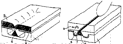
There is no known feasible way of producing a true thin-film
magnetic tape head with azimuth. A gap inclination (azimuth) can be
made only by mechanically machining the substrate. The aim of the
invention is to produce a thin-film magnetic tape head without
putting two half-blocks together. According to the invention, a
thin-film magnetic tape head (1, 6, 7, 8, 9) is produced in fifteen
process stages in which the "hour-glass effect" is of prime
importance. The process of the invention for producing a thin-film
magnetic tape head combines the advantages of planar thin-film
technology and gap production with the magnetic and mechanical
advantages of conventionally manufactured heads. Magnetic tape devices,
especially video recorders.
Note: Claims are shown in the official language in which they were submitted.
Note: Descriptions are shown in the official language in which they were submitted.
2024-08-01:As part of the Next Generation Patents (NGP) transition, the Canadian Patents Database (CPD) now contains a more detailed Event History, which replicates the Event Log of our new back-office solution.
Please note that "Inactive:" events refers to events no longer in use in our new back-office solution.
For a clearer understanding of the status of the application/patent presented on this page, the site Disclaimer , as well as the definitions for Patent , Event History , Maintenance Fee and Payment History should be consulted.
| Description | Date |
|---|---|
| Time Limit for Reversal Expired | 1994-10-17 |
| Application Not Reinstated by Deadline | 1994-10-17 |
| Deemed Abandoned - Failure to Respond to Maintenance Fee Notice | 1994-04-15 |
| Inactive: Adhoc Request Documented | 1994-04-15 |
| Application Published (Open to Public Inspection) | 1991-10-24 |
| Abandonment Date | Reason | Reinstatement Date |
|---|---|---|
| 1994-04-15 |
Note: Records showing the ownership history in alphabetical order.
| Current Owners on Record |
|---|
| DEUTSCHE THOMSON-BRANDT GMBH |
| Past Owners on Record |
|---|
| DIETMAR UHDE |

