Note: Descriptions are shown in the official language in which they were submitted.
~ BC9-91-090 1 2~8063~
ARBITRATION CONTROL LOGIC EOR Cu. Jl~C SYSTEM
ElAVING D~UAL BUS AR~
Ba~h~L~ d of the Invention
The present invention relates to bus to bus interfaces
in computer systems, and more particularly to improved
arbitration control logic and method for arbitrating control
of buses in a dual bus architecture computer system.
Generally in computer systems and especially in
personal computer systems, data is transferred between
various system devices such aa a central proces3ing unit
(CPU), memory devices, and direct memory access (DMA)
controllers. In addition, data is transferred between
expansion elements such as input/output (I/O) devices, and
between these I/O devices and t}le various system devices.
The I/O devices and the system devices communicate with and
amongst each other over computer buses, which comprise a
series of conductors along which information is transmitted
from any of several sources to any of several destinations.
Many of the system devi ces and t~le I/O devices are capable
of serving as bus controllers ( i e ., devices which can
control the computer system) and bus slaves (i.e., elements
which are controlled by bus controllers).
Personal computer systems having more than one bus are
known. Typically, a l~cal bus is provided over which the
CPU communicates with cache memory or a memory controller,
and a system I/O bus is provided over which system bus
devices such as the DMA controller, or the I/O devices,
communicate with the system memory via the memory
controller. The system I/O bus comprises a system bus and
an I/O bus connected by a bus interface unit. The I/O
devices communicate Wit~l one another over the I/O bus. The
I/O devices are also typically required to communicate with
system bus devices such as system memory. Such
0 BC9-91-ogo 2 2080~i30
communications must travel over both the I/O bus and the
system bus through the bus interface unit.
Often in computer systems it is necessary for expansion
devices to arbitrate fc~r owners~lip of the I/O bus of the
computer sy3tem; i.e., t:o decide wllich expansion device may
transfer information v:ia the I/O bus. It is known to
provide an arbiter which determines whicll expansion device
may transfer information via tlle I/O bu3, i.e., which
allocates the bus. Such an arbiter serves as a central
arbitration control pOi~lt: (CACP) via which all arbitration
for the I/O bus occurs.
The I/O bus operatea in time divided units which are
called bus cycles. Bus cycles of the I/O bus are divided
into arbitration cycles and grant cycles. During arbitration
cycles, expansion devices compete for ownership of the I/O
bu3. During grant cycles, a device which has won ownerahip
of the bus, transfers information.
I/O devices may only initiate memory read or write
cycles to system memory during an arbiter grant mode. Such
a method of serial arbitration imposel} performance
limitations on dual bus architecture computer systems due to
the time rec~uired to separately perform arbitration and the
memory read or write cycles which may occur only during an
arbiter grant mode.
It is an object of the present invention, then, to
provide an arbitration system and method for a dual bus
computer architecture system which simultaneously permits
(i) arbitration between a CPU and I/O devices contending for
control of I/O bus and (ii) completion of an I/O controller
device read or write operation to system memory or a CPU
write operation to expansion memory on an I/O slave device.
Sun~na]-y of the Invention
According to the pl~esent invention, arbitration control
logic and a method of arbitration are provided for a
0 BC9-91-o90 3 208~3~
computer having a dual bus architecture. The arbitration
control logic is implemented by algorithms which are built
into hardware in a }~U8 interface unit which resides
intermediate a sy3tem })us and an input/output bus in the
computer. The arbitration controL logic improves the
performance of the d~lal bus architecture computer by
permitting simultaneous arbitration cycle3 by a central
arbitration controller point and memory read and write
cycles by a CPU or I/0 devices.
The arbitration control logic operates under three
prescribed conditions. Under the first condition, an I/0
device desires to write data to system memory. After
completion of an arbitr.~tion cycle, the central arbitration
control point grants control of the I/0 bua ( and the system
bus via the bus interface unit) to the I/0 device. The I/0
device initiateEI one or more write cycles to system memory
which are temporarily stored in buffers in the bus interface
unit, before being written to system memory. Since the I/0
device may relinquish control of the I/0 bus at any time,
the bus interface unit may contain buffered data which still
needs to be written from the buffers out to system memory.
Although the I/0 device may relinquish control of the
I/0 bus, it mu3t remain in control of the system bus (via
the bus interface unit) to complete the write transfer of
the buffered data over the system bus to system memory. The
arbitration control logic in the bus interface unit
recognizes this condition and activates a CACP override
signal to the CACP requesting that it retain control of the
system bus. Accordingly, the central arbitration control
point begins a new the arbitration cycle simultaneously
while the buffered write data from the I/0 device is
transferred to system m~3~.0ry. Upon completing the buffered
write transfers, the CACP override signal is deactivated
allowing t~le CACP to complete arbitration and grant the I/0
bus .
The second condi tioll under which the arbitration
control logic in the buE: interface unit operates occurs when
2080~30
BC9-91-090
an I/O device desires to read data from 3ystem memory.
After completion of an arbitration cycle, the central
arbitration control point grant~i control of the I/O bu~ ( and
the ~ystem bus via the bu~ interface unit) to the I/O
device. The I/O device initiates one or more read cycles to
system memory. The bufl`ers in the bus interface unit are
continually filled wit~l prefetched data having addresses
contiguous to t}lo~e previously read. Once the I/O devlce
has read the last byte of data from the buffers it may
relinquish control of the I/O bu~ and thus the prefetched
data is not needed. Th~ls, the buffers in the bus interface
unit must be reset, effectively removing this unnecessary
data .
Although the I/O device may relinquish control o the
I/O bus at any time, it mu~t remain in control of the system
bu~ (via the bus interf~ice unit) until the current transfer
of data from system memory to the bus interface unit has
been completed. The arbitration control logic in the bu~
interface unit recognizes thi~ condition and activates a
CACP override signal to the CACP requesting that it retain
control of the system b~ls until t~le last prefetch operation
is completed and the buffers in the b~l~ interface unit are
reset. Accordingly, the central arbitration control point
begins a new arbitration cycle on the I/O bus ~imultaneously
while the bus interface unit complete~ the la~t prefetch
operation from system memory over the system bus and then
resets the buffers.
The third condition under which the arbitration control
logic in the bu~ interface unit operate~ occurs when a
sy~tem device such a~ the CPU is in control of the system
bu~ and de~ires to write data to an I/O device acting as a
~lave on the I/O bu~. After completion of an arbitration
cycle, the central arbiltration control point grants control
of the ~ystem bu~ ( and the I/O bus via the bus interface
unit) to the sy~tem device which initiates its write cycle
to the I/o device via the system bus to I/O bus tran~;lation
logic .
2080~30
BC9-91-090 5
The system bus to I/O bus translation logic provides a
buffer wherein data de~tined to be written from a system
device such as the CPU to expansion memory on an I/O 31ave
device is temporarily stored before being written to the I/O
slave device. After the last tranGfer of data is buffered
in the translation logic, the system bus is no longer
needed. The CPU and t~le bus interface unit indicate that
they are finished with the system bus. At this point, the
central arbitration controller may go into arbitration on
the I/O bus even though the data buffered in the translation
logic must still be written to t~le I/O device over the I/O
bus. This situation is pos3ible because, unlike I/O devices,
the CPU may write to an I/O device during either the
arbitration or grant modes of the central arbitration
controller .
The arbitration control logic in the bus interface unit
recognizes this condition and activates a CACP override
signal to the CACP requesting that it retain control of the
I/O bus until the last byte of buffered data is written to
the I/O device. Accordingly, t~le central arbitration
controller conducts tlle arbitration cycle simultaneously
while the data buffered in the translation logic is written
to the I/O device.
Brief Description of the Drawings
Figure 1 is a schematic block diagram of a computer system
incorporating a bus interface unit constructed according to
the principles of the present invention;
Flgure 2 is a schematic block diagram of the bus interface
unit of the computer syst~m of Figure l;
Flgure 3 is a schematic blGck diagram of the FIFO buffer of
the bus interface unit of Figure 2;
Figure 4 is a block circuit diagram of the CACP circuit and
bus interface unit of Figure l; and
20~0630
0 BC9-91-ogo 6
Figure 5 is a circuit diagram of one embodiment of the
arbitration control logic implemented in the bu~3 interface
unit of Eigure 1.
Detailed Description of the P~eferred F: ' - 'i L
Referring first to Figure 1, a computer system ~hown
generally at 10 comprisea 3ystem board 12 and processor
complex 14. ProceE~or complex includes processor portion 16
and base portion 18 conrlected at processor local bus 20 via
local bus connector 22. Proces~or portion 16 operates at 50
MHz and base portion 18 operate~ at 40 MHz.
System board 12 includes interleaved system memories
24 and 26 and input/output ( I/0) devices 28 . Communications
between memories 24 an~1 26 and processor complex 14 are
handled by memory bus 30, and communications between I/0
devices 28 and proce~soI^ complex 14 are carried by I/0 bus
32. Communications between I/0 devices and memories 24 and
26 are handled by I/0 b~ls 32, sy3tem bus 76 and memory bus
30. I/0 bus 32 may conform to MICR0 CHANNELR computer
architecture. Memory bus 30 and I~0 bus 32 are connected to
proce~sor complex base portion 18 via processor complex
connector 34. I/0 devices such as memory expansion devices
may be connected to the co;nputer system 10 via I/0 bus 32.
System board 12 may al~o include conventional video
circuitry, timing circuitry, keyboard control circuitry and
interrupt circuitry (none of which are s~lown) which may be
used by computer system 10 during normal operation.
Processor portion 3 6 of processor complex 14 includes
central processing unit (CPU) 38 which, in the preferred
embodiment, is a 32-bit l~icroprocessor available from Intel,
Inc. under the trade designation i486. Processor portion 16
also includes static ra~ldom access memory (SRAM) 40, cache
control module 42, fre~uency contrQl module 44, addres~
buffer 46 and data buffer 48. Local bus 20 comprises data
information path 50, address information path 52 and control
information path 54. Data information paths 50 are provided
between CPU 38, SRAM 40 and data buffer 48. Address
2080~30
BC9-91-090 =~ 7 ~
information path3 52 are provided between CPU 38, cache
control module 42 and address buffer 46. Control
information paths 54 are provided between CPU 38, cache
control module 42 and frequency control module 44.
Additionally, address and control information path~ are
provided between cache control module 42 and SRAM 40.
SRAM 40 provides a cache function by storing in short
term memory information from either system memories 24 or 26
or from expansion memory which is located on an I/O device
28. Cache control module 42 incorporate~3 random acce~s~
memory (RAM) 56 which store~ address locations of memories
24 and 26. CPU 38 may access information cached in SRAM 40
directly over the local bus 20. Frequency control module 44
synchronizes operation of the 50 Mhz processor portion 16
with the 40 MhZ base portion 18 and al~o controls the
operation of buffers 46 and 48 Accordingly, frequency
control module 44 determines the time~ at which information
is captured by buffers 46 and 48 or the times at which
information that is stored in these buffers is overwritten.
Buffers 46 and 48 are configured to allow two writes from
memories 24 and 26 to be stored simultaneously therein.
Buffers 46 and 48 are bi-directional, i.e., they are capable
of latching information which is provided by the CPU 38 and
information which is provided to ~he CPU. Because buffers
46 and 48 are bi-directional, p~ocessor portion 16 of the
processor complex 14 m,ay be replaced or upgraded while
maintaining a standard base portion 18.
Base portion 18 includes memory controller 58, direct
memory access (DMA~ controller 60, central arbitration
control point (CACP) circuit 62, bus interface unit 64 and
buffer/error correction code (ECC) circuit 66. Base portion
18 also includes driver circuit 68, read only memory (ROM)
70, self test circuit 72 and buffer 74. System bus 76
comprises a data information path 78, and address
information path 80 and a control information path 82. The
data information path connects buffer 74 with bus interface
unit 64; bus interface uni t 64 witl~ DMA controller 60 and
buffer/ECC circuit 66; and buffer/ECC circuit 66 with system
BC9-91-090 8 2080630
memories 24 and 26. The address information path and the
control information pat~l each connect memory controller 58
with DMA controller 60 and bus interace unit 64; and bus
interface unit 64 with buffer 74.
Memory controller 58 resides on both CPU local bus 20
and system buG 76, alld provides t~le CPU 38, the DMA
controller 60 or bu~ interface unit 64 ( on behalf of an I/O
device 28) with access to system memories 24 and 26 via
memory bus 30. The memory controller 58 initiates system
memory cycles to system memories 24 and 26 over the memory
bu~ 30. During a sy~tem memory cycle, either the CPU 38,
the DMA controller 60 or bus interface unit 64 (on behalf of
an I/O device 28) has access to ~ystem memories 24 and 26
via memory controller 58. The CPU 38 communicates to system
memory via local bus 20, memory controller 58 and memory bus
30, while the DMA controller 60 or bus interface unit 64 (on
behalf of an I/O device 28) acceas system memory via system
bu~ 76, memory controller 58 and memory bus 30.
For CPU 38 to I/O bus 32 read or write cycle~, address
information i~ checked againE;t ~y~tem memory address
boundarie3. If the address information corre~ponds to an
I/0 expansion memory a.ddress or I/O port addres~, then
memory controller 58 initiates an I/O memory cycle or I/O
port cycle with an I/O device 28 (via bus interface unit 64)
over the I/0 bus 32. During a CPU to I/0 memory cycle or
I/O port cycle, tlle ad.dres~ which is provided to memory
controller 58 i~ transmitted from system bus 76 to I/O bus
32 via bus interface unit 64 which resides intermediate
these t~o buses. The I/O device 28 which includes the
expansion memory to whi-h the address corre~pond~ receives
the memory addre~s from I/O bus 32 DMA controller 60 and
the bus interface unit 64 control the interchange of
information between system memorief; 24 and 26 and expansion
memory wllich i~ incorporated into an I/O device 28. DMA
controller 60 also pro~ides three functions on behalf of
processor complex 14. First, the DMA controller 60 utilizes
a small computer subsystem control block (SCB) architecture
to configure DMA channels, thus avoiding the necessity of
2~80630
BC9-91-090 9
using programmed I/0 to configure the DMA channels. Second,
DMA controller provides a buffering function to optimize
transfers between slow memory expansion devices and the
typically faster system memory. Third, DMA controller 60
provides an eight channel, 32-bit, direct system memory
access function. When l~roviding the direct system memory
acces~ function, DMA controller 60 may function in either of
two modes. In a first mode, DMA controller 60 functions in a
programmed I/0 mode in which the DMA controller is
functionally a slave to the CPU 38. In a second mode, DMA
controller 60 itself functions as a system bus master, in
which DMA controller 60 arbitrates for and controls I/0 bus
32. During this second mode, DMA controller 60 uses a first
in, first out (FIF0) register circuit.
CACP circuit 62 functions as the arbiter for the DMA
controller, I/0 device bus controllers and the CPU (if
accessing I/0 devices). CACP circuit 62 receives
arbitration control sigr~als from DMA controller 60, memory
controller 58 as well as from I/0 devices, and determines
which devices may control the I/0 bus 32 and the length of
time during which tlle particular device will retain control
of the I/0 bus.
Driver circuit 68 provides control information and
address information from memory controller 58 to system
memories 24 and 26. Driver circuit 68 drives this
information based upon lt~le rlumber of single in-line memory
modules (SIMMs) which are used to construct system memories
24 and 26. Thus, driver circuit 68 varies the signal
intensity of the control and address information which is
provided to system memories 24 and 26 based upon the size of
these memories.
Buffer circuit 74 provides amplification and isolation
betwee~l processor complex base portion 18 and system board
12. Buffer circuit 74 utilizes buffers which permit the
capture of boundary information between I/0 bus 32 and bus
interface unit 64 in real time. Accordingly, if computer
system 10 experiences a failure condition, buffer circuit 74
2080~30
BC9-91-090 10
may be accessed by a computer repair person to determine the
information which was present at connector 34 upon failure
of the system.
ROM 70 configures the system lO upon power-up by
initially placing in ~ystem memory data from expansion
memory. Self test cir~uit 72, which is connected to a
plurality of locations within base portion 18, provides a
plurality of self test features. Self test circuit 72
accesses buffer circuit 74 to determine if failure
conditions exist, and alao tests the other major components
of base portion 18 upon power-up of the system 10 to
determine whether the system is ready for operation.
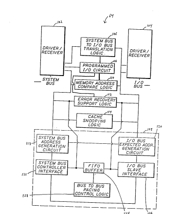
Referring to Figure 2, a schematic block diagram of the
bus interface unit 64 of the system of Figure 1 is shown.
Bus interface unit 64 provides the basis for implementation
of the pre3ent invention by providing a bi-directional high
~peed interface between æystem bus 76 and I/O bus 32.
Bus interface ~mit 64 include3 system bu3
driver/receiver circuit 102, I/O b~is driver/receiver circuit
104 and control logic circuits electrically connected
therebetween. Driver~recQiver circuit 102 includes steering
logic which directs signals received from the system bus 76
to the appropriate bus interface unit control logic circuit
and receives signals f~om the bua interface unit control
logic clrcuits and directs the signals to the 3ystem bus 76.
I/O bus driver/receiver circuit 104 includes steering logic
which directs signals received from the I/O bus 32 to the
appropriate bus interface unit control logic circuit and
receives signals from tlle bus interface unit control logic
circuits and directs the signals to the I/O bus 32.
The bus interface Imit control logic circuits include
system bus to I/O bus translation logic 106, I/O bus to
system bus translation logic 108, memory address compare
logic 110, error recovery support logic 112, and cache
snooping logic 114. Programmed I/O circuit 116 is also
electrically coupled to system driver/receiver circuit 102.
2080S30
0 BC9-91-090 11
The system bus t o I/0 bus translation logic 106
provides the means required for the DMA controller 60 or the
memory controller 58 (on behalf of CPU 38) to act as a
system bus controller to access the I/0 bus 32 and thereby
communicate with I/0 devices 28 acting as slave devices on
the I/0 bus. Translation logic 106 translates the control,
address and data lines of the system bus 76 into similar
lines on the I/0 bus 32. Most control signals and all
address signal3 flow from the system bus 76 to the I/0 bus
32 while data information flow is bi-directional. The logic
which acts as system bus slave monitors the system bus 76
and detects cycles which are intended for the I/0 bus 32.
Upon detection of 8UC~I a cycle, the system bus slave
translates the timing o~ signals on the system bus to I/0
bus timing, initiates th,2 cycle on the I/0 bus 32, waits for
the cycle to be completed, and terminates the cycle on the
system bus 76.
The I/0 bus to 3ystem bus translation logic 108
comprises system bus address generation circuit 118, I/0 bus
expected addres3 generation circuit 120, system bus
controller interface 122, FIF0 buffer 124, I/0 bus slave
interface 126 and bus to bus pacing control logic 128.
System bus controller interface 122 supports a high
performance 32 bit (4 by~e) i486 b~lrst protocol operating at
40 MHZ. Data transfers of four, eight and sixteen bytes in
burst mode and one to four bytes in no-burst mode are
provided. I/0 bus slave interface 126 monitors the I/0 bus
32 for operations destir~ed for slave devices on the system
bus 76 and ignores those operations destined for the I/0 bus
32. All cycles picked U]? by the I/0 bus slave interface 126
are passed on to the FIF0 buf~er 124 and the system bus
controller interface 122.
The I/0 bus to system bus translation logic 108
provides the means required for an I/0 device 28 to act a3
an I/0 bus controller t~ access system bus 76 and thereby
read or write to system memories 24 and 26. In either of
these operations, an I/0 device controls the I/0 bus. The
asynchronous I/0 bus interface 126, operating at the speed
2080630
BC9-91-090 12
of the I/O device, permits the bus interface unit 64 to act
as a slave to the I/O device controller on the I/O bus 32 to
decode the memory addre ss and determine that the read or
write cycle is destined for system memories 24 or 26.
Simultaneously, the sy~tem bus controller interface 122
permits the bus interface unit 64 to act as a controller on
the system bus 74. The memory controller 58 (Figure 2~ act3
aa a slave to the bus interface unit 64, and either provides
the interface 64 with data read from system memory or writes
data to system memory. The reads and writes to system
memory are accomplished through the FIFO buffer 124, a block
diagram of which is illustrated in Figure 3.
As shown in Figure 3, EIFO buffer 124 is a dual ported,
asynchronous, bi-directional storage unit which provides
temporary storage of data information between the system and
I/O buses 76, 32. FIFO buffer 124 comprises four
sixteen-byte buffers 125A-125D and FIFO control circuit 123.
The four buffers 125A-125D buffer data to and from I/O bu3
controllers and system bus slaves, thereby allowins~
simultaneous operation of the I/O bus 32 and the system bus
76. The FIFO buffer 124 is physically organized as two
thirty-two byte buffers (125A/125B and 125C/125D). The
system bus controller interface 122 and the I/O bus slave
interface 126 each control one thirty-two byte buffer while
the other thirty-two byte b~lffer operates transparent to
them. Both of t~le thirty-two byt~ buffers are utilized for
read and write operations.
Each FIFO 124A, 125B, 125C, 125D has an address
register section either physically associated with the
respective FIFO, or logically associated therewith. As data
is transferred from the I/O bus 32 to FIFO 125A, the data
will be accumulated until the 16 byte buffer is filled with
16 bytes of data, provided that the addresses are
contiguous. If a non-contiguous address is detected by the
address action, the FIFO 125A will transfer the stored data
to FIFO 125C, and at the same time FIFO 125B will start to
receive this data from tho= llew non-contiguous address. FIFO
125B Will continue just as FIFO 125A did until it is filled
208063~
BC9-91-090 13
with 16 bytes of data, or another non-contiguous address is
detected. FIF0 125B will then transfer the atored data to
FIF0 125D. and FIF0 125l~ again starts to 3tore data; thus,
it is possible to 3tore up to four 16 byte blocks of non-
contiguous address data.
Further, by having two 32 byte buffers in parallel the
reading and writing of data can be toggled between them thus
giving an es3entially continuous read or write function.
Moreover, by splitting the 32 byte buffers into two 16
bytes buffer sections which are coupled to other ~/0 bus 32
or system bus 26, the number of storage buffers can be
increased with minimal impact on tlle performance of the FIF0
a3 related to the capacitive loading on signal~ clocking
data in or out of the storage registers. This is
accomplished because for every two buffers added (in
parallel) only half the capacitive loading is added to the
loading of clock signal3 on each bus.
Additionally, by having two 16 byte buffers in series
in each leg, once one o the 16 byte buffer3 is filled with
data, such as in a read operation, the data can be
transferred to the other 16 byte buffers in series
therewith, while the ot~ler parallel leg is accumulating
data. Hence, there is no time lost in either accumulating
data, or transferring the data from one bus to the other.
The logic for controlling the operation of the FIF0 124
is supplied by FIF0 Control Circuit 123
A particular I/0 device 28 may write to ~y~tem memories
24 or 26 via I/0 bus in bandwidths of either 1, 2 or 4 bytes
(i.e., 8, 16 or 32 bits) During writes to system memory by
an I/0 device 28, the first transfer of write data is
initially stored in the FIE0 buffer 125A or 125B. The I/0
bus expected address generation circuit 120 calculates the
next expected, or contiguous, address. The next contiguous
address iæ checked agai nst the subsequent I/0 address to
verify if the subse~[uent transferæ are contiguous or not.
~ BC9-91-090 14 2080630
If contiguous, the second byte or bytes of write data i3
sent to the same FIFO buffer 125A or 125B. The FIFO
receives data at asynchronous speeds of up to 40 megabytes
per second from the I/O bus 32.
This process continues until either buffer 125A or 125B
is full with a 16-byte packet of information or a
non-contiguous address i s detected . On the next clock
cycle, assuming that buffer 125A is full, the data in buffer
125A is transferred to buffer 125C. Similarly, when buffer
125B is full, all of it1 contents are transferred to buffer
125D in a single clock cycle. The data stored in the buffers
125C and 125D is then written to system memory via an i486
burst transfer at the system bus operational speed. The
operation of FIFO buffer 124 during a write to system memory
by an I/O device is tilus continuous, alternating between
buffers 125A and 125B, with each emptying into adjacent
buffer 125C or 125D, respectively, while the other is
receiving data to be written to system memory. The FIFO
buffer 124, then, opti~nizes the speed of data writes to
system memory by ~ i ) anticipating the address of the next
likeLy byte of data to be written into memory and (ii~
accommodating the maxim~lm speed of write data from the FIFO
buffer to system memory via the system bus 76.
During reads of data from system memory to an I/O
device 28, FIFO buffer 124 operates differently. The system
bus address generation circuit 118 uses the initial read
address to qenerate sub~e~[uent read addresses of read data
and accumulate data in buffer 125C or 125D. Because the
system bus supports transfers in bandwidths of 16 bytes
wide, the system bus controller interface 122 may prefetch
16-byte packets of contiguous data and store it in buffers
125C or 125D without Izhe I/O bus 32 actually providing
subsequent addresses, thus reducing latency between
transfers. When buffer 125C is full of prefetched data, it
transfers its contents to buffer 125A in one clock cycle.
Buffer 125D similarly empties into buffer 125B when full.
The data in buffers ~25A and 125B may then be read by a
particular I/O device controller in ~andwidths of 1, 2 or 4
2Q8~630
BC9-91-090 15
bytes. In this way, system bus address generation circuit
118 functions as an incr,r~ment counter until instructed to by
the I/0 controller device to stop prefetching data.
Bus to bus pacing control logic 128 creates a faster
access to system memory for high speed I/0 devices. The bus
to bus pacing control logic 128 overrides the normal memory
controller arbitration scheme of system 10 by allowing an
I/0 device in control of the I/0 bus 32 uninterrupted access
to system memory during transfers of data by faster devices
which require multiple cycles, rather than alternating
access to the memory controller 58 between the I/0 device
and the CPU. Thus, even if a local device such as the CPU
has a pending rer~uest for control of the memory bus during a
multiple cycle transmission by an I/0 device, the bus to bus
pacing control logic 128 will grant the I/0 device continued
control of the memory bus.
The programmed I/0 circuit 116 is the portion of the
bus interface unit 64 which contains all of the registers
which are programmable within the bus interface unit 64.
The registers have bitE~ associated therewith to determine
whether a particular register is active or inactive. These
registers define, inter alia, the system memory and
expansion memory addresE3 ranges to which the bus interface
unit 64 will respond, the expansion memory addresses which
are either cacheable or noncacheable, the system memory or
cache address ranges, and whether or not parity or error
checking is supported by the bus interface unit.
Accordingly, programmed I/0 circuit 116 identifies for the
bus interface unit 64 the environment in which it resides,
and the options to which it is configured. The registers in
programmed I/0 circuit 116 cannot be programmed directly
over the I/0 bus 32. Hence, in order to program the system
10, the user must have access to an I/0 device which may
communicate over t~le system bus to the programmed I/0
circuit 116 at the CPU level.
Memory address compare logic 110 determines if a memory
address corresponds to system memory or corresponds to
2080630
BC9-91-090 16
expansion memory which is located on I/O device 28 coupled
to the I/O bus 32. Because the system memory as well as the
expansion memory may be in non-contiguous blocks of
addresses, memory address compare logic 110 includes a
plurality of comparators which are loaded with boundary
information from registers in the programmed I/O circuit 116
to indicate which boun~laries correspond to which memory.
After a particular memory address is compared with the
boundary information by the memory address compare logic,
the bus interface unit is prepared to react accordingly.
For example, if an I/O cLevice controlling the I/O bus 32 is
reading or writing to expansion memory, the bus interface
circuit need not pas~ that address to the memory controller
58, thereby saving time and memory bandwidth.
Error recovery support logic 112 permits the system 10
to continue operation~ even if a data parity error i8
detected. On any read or write access by an I/O device 28
to system memories 24 or 26, parity of the data is checked.
Support logic 112 in-teract8 with a register in the
pro~l ?d I/O circuit 116 for capturing the address and the
time of the detected parity error. The contents of this
register may then be acted UpOII by appropriate system
software. Eor example, t~le CPU 38 may be programmed for a
high level interrupt to pull the addres~ out of the register
at any time a parity error is detected. The CPU may then
decide, based on the system software instructions, whether
to continue system operc~tions or merely terminate operation
of the identified source of the parity error.
Cache snooping logic 114 permits the bus interface unit
64 to monitor the I/O bus 32 for any writes to expansion
memory by an I/O device taking place over the I/O bus 32.
The snooping logic fi rst determines if the write to
expansion memory occurred in expansion memory which is
cacheable in SRAM 40 If it is not cacheable expansion
memory, there is no danger of corrupt data being cached.
If, however, a positive compare indicates that the write
occurred in cacheable expansion memory, a cache invalidation
cycle is initiated over the system bus 76. The CPU is thus
2~8063~
BC9-91-090 17
instructed to invalidate the corresponding addresE} in SRAM
40. Cache snooping logic 114 provides means to store the
address of a po3itive compare 80 that snooping of the I/O
bus may continue immediately after detection of the first
positive compare, thereby permitting continuou~ monitoring
of the I/O bus 32.
The present invention relates generally to the bu3
interface unit 64 described above and more particularly to
system bus arbitration control logic 130 (Figure 5) which is
contained within the bus interface unit 64 residing
intermediate the sy3tem bus 76 and the input/output bus 32
in the computer system 10. The arbitration control logic
interacts with CACP circuit 62 which alternates between
arbitration cycles and c~rant cycles. The operation of the
CACP circuit 62 is dec;cribed in copending U. S. Patent
Application Serial No. 07/777,777, filed October lS, 1991,
entitled "CONTROLLING BUS ALLOCATION USING ARBITRATION
HOLD". The arbitration control logic 130 in the bus
interface unit 64 improves the performance of the dual bus
architecture computer fiystem by permitting arbitration
cycles by CACP circuit ~2 to sim~llta~leo~lsly overlap memory
read and write cycles by the C~ll 38 or I/O device 28.
Figure 4 shows the system interconnection of I/O bus
32, system bus 76, CACP circuit 62 and bus interface unit
64 .
The multiple transfer request line 144 provides the
means by which an I/O device 28 already in control of the
I/O bus 32 indicates it is ready to perform more than one
transfer of data over the l/O bus 32. The CACP responds to
this request by maintairing I/O bus 32 in a grant mode for
the I/O device until all of the multiple transfers of data
have been completed over the I/O bus 32. Upon completion of
the multiple transfer over the I/O bus, the I/O device
deactivate~ line 144 and the CACP circuit 62 determines that
the I/O device is off of the I/O buF- 32 rmd begins the next
arbitration cycle 132. The arbitration control logic 130
within bus interface un:it 64, as will be explained below,
2~8~63~
* BC9-91-090 18
provides a CACP overrid.e signal 146 to the bus interface
unit 62 to prevent the CACP circuit from re-entering grant
mode while activity is occurring over the system I/O bus.
Only when CACP override signal 146 is driven inactive may
the CACP circuit 62 enter the next grant cycle.
The arbitration control logic 130 operates under three
prescribed conditions. Under the first condition, an I/O
device in control of the I/O bus 32 writes a multiple
transfer of data to system memories 24 and 26 over the I/O
and system buses 32, 76. Under the second condition, an I/O
device in control of the I/O bus 32 reads a multiple
transfer of data from system memories 24 and 26 over the I/O
and system buses. Under the third condition, a system
device such as the CPU 38 which is in control of the system
bus 76 writes data to an I/O device acting as a slave on the
I/O bus 32. In each of these three particular operations,
arbitration by CACP circuit 62 is permitted to proceed
before the operation has gone to completion, thereby
allowing simultaneous arbitration by CACP circuit 62 on the
I/O bus and completion of tlle particular operation.
Each of t~le three conditions under which the
arbitration control logic 130 operates will now be explained
in greater detail. Under the first condition, an I/O device
28 desires to write data to system memories 24 and 26.
After completion of an arbitration cycle, CACP circuit 62
grants control of the I~O bus 32 ( and t~le system bus 76 via
the bus interface unit 64) to t~le I/O device 28. The I/O
device initiates one or more write cycles to system memories
24 and 26 which are temporarily stored in FIFO buffers 125A
and/or 125B. Since I/o ~evice 28 may relinquish control of
I/O bus 32 at any time, the bus interface unit may contain
buffered data which still needs to be written from buffers
125A and/or 125B to bu Efers 125C and/or 125D and out to
system memories 24 and 26.
Although the I/O d~vice 28 may relinquish control of
the I/O bus 32, it must remain in control of the system bus
76 (via the bus interfa.ce unit 64) to complete the write
2080630
BC9-91-O9O 19
tran3fer of buffered data over the sy3tem bu3 76 to 3ystem
memorie3 24 and 26. The arbitration control logic activate3
130 in the bu3 interface unit recognize3 thi3 condition and
activate3 a CACP override 3ignal 146 to CACP circuit 62
reque3ting that it retain control of the ~y3tem bu3 76 (via
the bu3 interface unit 64). Accordingly, CACP circuit 62
begin3 the arbitration cycle 3imultaneou31y while the write
data buffered in FIFO ]~uffer 124 from the I/O device i3
tran3ferred to 3y3tem memorie3 24 and 26. A3 long a3 the
arbitration control logic 130 continue3 to activate the CACP
override 3ignal 146, CAC'P circuit 62 will not grant acce33
to the 3y3tem bu3 76 to another I~O device 28. Thi3 will
occur until the la3t tra]~3fer of b~lffered write data i3 made
to æy3tem memory After ~hich the arbitration control logic
130 will deactivate the CACP override 3ignal 146 which
allow3 the CACP 62 to complete arbitration and grant the I/O
bu3 32 to a new I/O device 28. Thi3 avoid3 contending
operation3 on the 3y3tem bu3 76. I/O device3 in control of
the I/O bu3 32 may initiate cycle3 on the I/O bu3 only when
CACP circuit 62 i3 in grant mode.
The 3econd conditioIl under which the arbitration
control logic 130 in the bu3 interface unit 64 operate3
occur3 when an I/O device 28 desire3 to read data from
3y3tem memorie3 24 arld 26. ~fter completion of an
arbitration cycle, CACP circuit 62 grant~ control of the I/O
bu3 32 (and the 3y3tem bll3 76 via t~le bus interface unit 64~
to the I/O device 28. The I/O device 28 initiate3 one or
more read cycle3 to ~y3tem memorie3 24 and 26. The EIFO
buffer3 125C and/or 125D are continually filled with
prefetched contiguou3 data in the manner explained in the
de3cription of the FIFO buffer 124 above. Once the I/O
device 28 ha3 read the la3t byte of data from the FIFO
buffer3 125A and/or 125~ it will relinqui3h control of I/O
bu3 32 and thu3 the data prefetched into buffer~ 125C and
125D i3 not needed. Thu3, the FIFO 124 mu3t be re3et,
effectively removing thiJ3 unnecea3ary data.
Although the I/O device 28 may relinqui3h control of
the I/O bu3 32 at any time, it mu3t remain in control of the
2~8~63~
BC9-91-090 20
system bus 76 (via the bus interface unit 64) until the
memory controller 58 indicates t}lat it has completed the
current transfer of data from system memories 24 and 26 to
the bus interface unit 64. The arbitration control logic
130 in the bus interface unit recognizes this condition and
activates the CACP override signal 146 to CACP circuit 62
requesting that it retain control of the system bus 76 (via
the bus interface unit 64) until the last prefetch operation
is completed and the EIE'0 buf~er 124 is reset. Accordingly,
CACP circuit 62 begins a new arbitration cycle on the I/0
bus 32 simultaneously while the bus interface unit 64
complete3 the last prefetch operation from system memory
over the system bus 76 and theJ~ resets the FIF0 buffer 124.
As long as the arbitration control logic 130 continues to
activate the CACP override signal 146, CACP circuit 62 will
not grant access to the system bus 76 to another I/0 device
28. This will occur until the prefetch and reset operations
are completed over the system bus after which the
arbitration control lo~Jic 130 will deactivate the CACP
override signal 146 which allows the CACP 62 to complete
arbitration and grant the I/0 bus 32 to a new I/0 device 28.
This avoids contending operations on the system bus 76.
The third condition under whlch t~le arbitration control
logic 130 in the bus interface unit operates occurs when a
system device such as the CPU 38 in control of the system
bus 76 and desires to write data to an I/0 device 28 acting
as a slave on the I/0 bus 32 After completion of an
arbitration cycle, CACP circuit 62 grants control of the
system bus 76 (and the I/0 bus 32 via the bus interface unit
64~ to the system device which initiates its write cycle to
the I/0 device 28 via the syste~n bus to I/0 bus translation
logic 106.
The system bus to I/0 bus translation logic 106
provides a buffer (not shown) wherein data destined to be
written from a system device such as the CPU 38 to expansion
memory on an I/0 slave d~vice is temporarily stored before
being written to the I/0 slave device. After the last
tranufer of data is buf~ered in trallslation logic 106, the
system bus 76 is no longer needed. The CPU 38 indicates
2~8~63~
BC9-91-090 21
that it i8 finished witll the system bus 76 as does the bus
interface unit 64, however, the arbitration control logic
130 will activate the CACP override signal 146 to inform the
CACP 62 that it needs to retain control of I/O bus 32. At
this point, CACP circuit 62 may go into arbitration on the
I/O bus 32 even though the buffered data in translation
logic 106 must still be written to the I/O device over the
I/O bus 32. This situation is possible because, unlike I/O
devices, the CPU 38 may l,rrite to an I/O device during either
the arbitration or grant modes of CACP circuit 62.
Accordingly, CACP circuit 62 conducts the arbitration
cycle simultaneously while the buffered data in translation
logic 106 is written to the I/O device, after which the
arbitration control logic 130 will deactivate the CACP
override signal 146 which allows the CACP 62 to complete
arbitration and grant the I/O bus 32 to a new I/O device 28.
This avoids contending operations on the I/O bus between the
CPU 38 and an I/O device 28.
One embodiment of the arbitration control logic 130
within the bus interface unit 64 is shown in Figure 6. The
arbitration control logi.c 130 is implemented by algorithms
which are built into th~ hardware of the bus interface unit
64. Arbitration control logic 130 comprises AND gate 148
and S-R latches 150 and 152. As explained above, the CACP
override signal 146 is output by ~he arbitration control
logic 130 when an I/O device in control of the I/O bus 32
reads or writes a multiple transfer of data from or to
system memories 24 and 26 over the I/O and system buses 32,
76. CACP override sigr~al 146 is negative active. ~ence,
during an I/O device read from system memories 24 and 26,
data is prefetched from system memory into EIFO buffer 124
and read prefetch begin~ line 154 is driven HIGH, setting
latch 150. The complemented output 156 of latch 150 goes
LOW, activating the CACP override signal 146, and preventing
the CACP circuit 62 from performing its next grant cycle
while data is prefetched over the system bus 76. The I/O
device retains control of the system bus (via the bus
interface unit 64) until the read prefetch operation is
BC9-91-090 22 2~80630
complete. When the recld prefetch operation is complete,
line 158 i8 driven HIGH, resetting latch 150 and
deactivating the CACP override signal 146. The CACP circuit
62, which by now has entered the arbitration mode, is
permitted to enter the n,-xt grant mode.
During an I/O device write to system memories 24 and
26, data is first writte~ into FIFO buffer 124 and the write
to system memory line 160 is driven HIGH, thereby setting
latch 152. The complemented output 162 of latch 152 goes
LOW, activating the CACP override signal 146, and preventing
the CACP circuit 62 from entering its next grant cycle while
data is being written from FIFO buffer 124 to 3y3tem memory
over the sy3tem bus 76. The I/O device retains control of
the sy3tem bus (via the bus interface unit 64) until the
write to system memory :is complete. The I/O bus, however,
is available for simultaneou~ arbitration proce33es by the
CACP circuit 62. CACP override signal 146 prevents the CACP
circuit from re-entering the grant mode. Upon completion of
the write operation, all of the buffers in FIFO buffer 124
will be empty, driving line 164 HIGH and resetting latch
152. CACP override signal 146 will be deactivated,
enabling the CACP circui t 62 to eIlter grant mode.
I~uring a system de~ice (such as the CPU 38), write to
an I/O device 28, the data is temporarily stored in a buffer
provided by I/O bus translation logic 106. Upon storing the
data, I/O bus translation logic 106 will drive the posted
CPU cycle signal 166 low, activating the CACP override
signal 146, as well as informing system bus 76 that the
write cycle has been completed. This allows additional
operations to occur on system bus 76 while I/O` bus
translation logic 106 co]npletes writing the buffered data to
I/O device 28. Upon completing the write operation to I/O
device 28, I/O bus translation logic 106 will drive the CPU
posted cycle signal 166 ~IIGH, thereby deactivating the CACP
override signal 146, ~hich allows CACP 62 to complete
arbitration and grant I/O bus 32 to a new I/O device 28.
2080
~ BC9-91-090 23 630
Accordingly, the preferred embodiment of a bus control
logic system for computers having dual bus architecture haa
been described. With the foregoing description in mind,
however, it is understood that t~ description i~ made only
by way of example, that the invention i~ not limited to the
particular embodiments described herein, and that variou3
rearrangements, modification~, and substitution~ may be
implemented without departing from the true spirit of the
invention a~ hereinafter claimed.