Note: Descriptions are shown in the official language in which they were submitted.
BACKGROUND OF THE INVENTION
1. Field of the Invention
This invention relates to optical modulators and switches, more particularly
to integrated optic waveguide modulators and switches.
2. Backsround of the Invention
Anti-resonant Reflecting Optical Waveguides (ARROW) have several
advantages over other types of waveguides. They can be formed upon silicon,
using
relatively thin layers compared to other waveguides, for easier compatibility
with
other electronic integrated circuits. At the same time, they can have a large
mode
for coupling to optical fibers. Additionally, they are relatively easy to
manufacture,
as they require no exotic materials.
These waveguides typically consist of a layer of silicon oxide built upon a
silicon substrate. An interference layer of silicon is then placed upon the
first Iayer
of silicon oxide, followed by another layer of silicon oxide. All of these
materials can
be deposited with relative ease. The silicon layer sandwiched between the two
silicon
oxide layers functions as a passive interference cladding layer. The thickness
of the
interference layer is not critical.
Vertical coupling has been achieved in such layered structures made of
semiconductor materials by the use of periodic gratings in the materials that
make
up the structure. This technique can be used to couple light between the top
core
layer and the interference layer.
Active optical modulators are normally difficult to produce in or on silicon.
TI-16601 Page 1
20g06'~2
Silicon exhibits no linear electro-optic effect, although changes in
absorption or
refractive index may be induced by modulating the density of free carriers.
All-silicon
waveguides tend to have a high propagation loss due to these same free-carrier
effects
and are difficult to fabricate to have a high modulation efficiency, because
of poor
modal overlap. All-dielectric waveguides can have low loss, but are typically
passive
and not useful for modulation. Using an ARROW structure in conjunction with
vertical coupling will make it possible to combine the low-loss propagation of
dielectric waveguides with the capability of modulating or switching light
using free-
carrier effects.
TI-16601 Page 2
20806'2
SUMMARY OF THE INVENTION
Objects and advantages will be obvious, and will in part appear hereinafter
and
will be accomplished by the present inv ention which provides an optical wav
eguide
modulator or switch. The waveguide is an Anti-Resonant Reflecting Optical
Waveguide with one interference layer of a semiconductor material between two
layers of dielectric material. Free-carrier effects in the interference layer
are
controlled by application of a current or field to an active electronic
element in the
layer to modulate light in the layer.
TI-16601 Page 3
2080672
BRIEF DESCRIPTION OF THE DRAWINGS
For a complete understanding of the invention, and the advantages thereof,
reference is now made to the following description in conjunction with the
accompanying drawings, in which:
FIGURE 1A shows a side view of an ARROW waveguide adapted to modulate
light using free-carrier effects.
FIGURE 1B shows an end view of an ARROW modulator adapted to control
free-carrier effects.
FIGURE 2A shows a path of light flowing through an ARROW modulator.
FIGURE 2B shows a top view of an ARROW modulator with a transistor for
controlling free-carrier concentration in a semiconductor interference layer.
FIGURE 2C shows an end view of an ARROW modulator with a transistor for
controlling free-carrier concentration in a semiconductor interference layer.
FIGURE 3A shows a side view of another ARROW waveguide adapted to
modulate light using free-carrier effects.
FIGURE 3B shows an end view of an alternate embodiment of an ARROW
waveguide adapted to modulate light using free-carrier effects.
FIGURE 4 shows a manufacturing process that could be used to form an
ARROW waveguide device adapted to modulate light using free-carrier effects.
TI-16601 Page 4
DETAILED DESCRIPTION OF THE PREFERRED EMB
A side view of an ARROW modulator that uses the free-carrier effect in
semiconductors is shown in Figure 1A. The modulator 10 consists of a substrate
12,
which is usually, but not limited to, silicon. Substrate 12 has a doped or
deposited
area 14, which forms the gate of a transistor. The placement of the source and
the
drain of the transistor will be covered in further discussion.
Upon the substrate is the lower cladding of the waveguide, 16. This is
normally silicon oxide. On top of the lower cladding layer is the interference
layer,
18, which, in this example, is silicon. Other semiconductor materials may also
be
used. The interference layer thickness must be such that constructive
interference
between the reflections from the top and bottom surfaces of this layer occurs
to
provide high reflectivity for the mode guided in the core layer.
Periodic gratings 22 and 24 have been formed into the top of the interference
layer 18. This can be accomplished by many ways, including etching. Although
shown as two separate gratings, they could also be the two ends of a long
section of
grating. These gratings allow vertical coupling between the core arid the
interference
layer. The core layer, 20, is deposited upon the interference layer, and is
typically
made out of a dielectric material with high optical transparency, such as
silicon oxide,
or silicon nitride. The Lower cladding layer is chosen to be approximately one-
half the
thickness of the core, to prevent waveguiding in this layer.
Figure 1B shows an end view of one embodiment of the modulator 10.
Substrate 12 has, in addition to gate 14, source contact 26 and drain contact
28. The
TI-16601 Page 5
2080672
lower cladding 16 is deposited and etched, or just deposited, in such a manner
as to
allow the interference layer 18 to "touch down" and come in contact with the
substrate 12, and its source and drain contacts. This contact allows the
modulator
to be controlled, if desired, by circuitry in the substrate. Alternatively,
contact may
be made from the top through the core layer. As the core layer 20, has a
waveguide
rib, or other structure to transversely confine the light 30, the cladding
underneath
the edges of the core is not really necessary anyway. This allows for more
freedom
in the process design to manufacture the modulator.
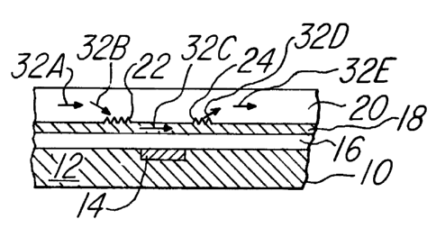
Figure 2A shows the path of light through the modulator. The light enters the
core layer 20 from the left of the drawing, shown as arrow 32A. The light
travels
over the grating 22 and is coupled by and through the grating into the
interference
layer 18, as shown by arrow 32B. Since the interference layer has a higher
refractive
index than the surrounding core and cladding layers, it acts as a conventional
dielectric waveguide for light traveling within it. While the light is in the
interference layer, shown by arrow 32C, control circuitry, or a control
element, as will
be discussed, can be used to control the free-carrier concentration, and
thereby
modulate the light. One method for achieving this is to dope the interference
layer
to form source and drain regions, and to then apply voltage to gate 14. Then,
if the
resulting transistor is turned off, the free-carrier concentration between the
source
and drain regions will drop drastically in the silicon. The transistor may
conceivably
be operated in either the depletion or the enhancement mode. In either case,
the
changes in free-carrier concentration will result in changes in the refractive
index
TI-16601 Page 6
20806'2
experienced by Light. guided in the interference layer. For example, an
increase in the
free-carrier concentration will r esult in a decrease in the refractive index
for light at
the 1.3 pm wavelength.
The control of the carrier concentration between the source and drain allows
for control of the light that will eventually couple out of the interference
layer. The
previously passive layer of silicon has been turned into an active element for
modulating light.
Lateral confinement for light traveling in this layer is desirable for
efficient
coupling back into the laterally-confined core layer mode. This may be
provided, for
example, by doping the interference layer to change its refractive index. For
example,
germanium could be used for raising the refractive index of a silicon layer.
The
doping forming the control element may also contribute to lateral confinement.
A possible placement of the source and drain regions is shown in Figure 2B,
a top view of a modulator. The core layer 20 is seen from above, with rib 30
in the
middle. Gratings 22 and 24 are shown in dashed lines. These gratings are shown
etched onto the interface between the core and interference layers. The
preferred
placement for the gratings is on the surface of the interference layer, but
they may
be formed in the material either of the interference layer, or of the core
layer. Source
27 and drain 29 are in the interference layer, and are hatched to show the
active area
in the silicon between them. Gate 14 is under this region, in or on the
substrate
below the lower cladding layer. It is hatched differently to highlight its
location.
Light will be modulated or absorbed depending on the state of the transistor,
ON or
TI-16601 Page 7
OFF. 2080672
Figure 2C shows an end view of this structure. Source 27 and drain 29 are of
the same doping, either n-type or p-type, demonstrated by identical hatching.
The
gate region 14 is typically in the substrate, as in this case, and under the
undoped
region between the source and drain regions. The gate must be isolated
electrically
from the source and drain. As discussed previously, the application of voltage
to this
control element is used to manage the free-carrier concentration.
Additionally,
contact regions for the source and drain could be placed in the substrate 12,
under
regions 27 and 29, where these regions contact the substrate 12.
Another embodiment for control of the free-carrier effects is shown in Figures
3A and 3B. A top view of such an embodiment is shown in Figure 3A. Instead of
the
transistor in the interference layer as shown previously, a p-i-n diode could
be used.
The entire region that comprises the p-i-n diode has been shaded for viewing
clarity.
P-doped region 34 has a lower boundary at the upper edge of the confinement
structure 30, as seen on the drawing. The i region 36 is undoped, and lies
under the
confinement structure 30. The n-doped region 3$ has an upper boundary at the
lower
edge of confinement structure 30, as seen on the drawing. Note that since p-
type and
n-type doping both reduce the refractive index, this structure also provides
for lateral
optical confinement in the intrinsic region of the interference layer. The p-i-
n diode
structure is actually easier to manufacture and allows for better control of
the carrier
concentration, than the configurations previously discussed.
An end view of this structure is shown in Figure 3B. Layer 20 is shown with
TI-16601 Page 8
2~sos7~
the confinement structure 30. Region 34, the p-doped region, is to the left of
the
confinement structure, in the interference layer. The interference layer is
shown
making contact with the semiconductor substrate 12. This is only for
electrical
connection ease, and better integration of the device. There is no optical
reason for
this, and this should not be considered as such in the design process.
The p-i-n diode structure controls the free-carrier concentration in the
following
way. When the structure is reverse biased, the intrinsic region in the
interference
layer is depleted of carriers. When the structure is forward biased, carriers
are
injected into this region continuously, where they recombine, allowing current
to flow.
Figure 4 shows a process for manufacture for one embodiment of the invention.
The first step, 40, is to prepare a silicon, or other semiconductor material,
substrate.
The substrate could be silicon, gallium arsenide, or other semiconductor
material, and
may or may not contain electronic control circuitry. The next step, 42, is to
form the
lower cladding, usually out of silicon oxide, or silicon nitride. There are
many ways
in which to form this layer, one of which is to use thermal oxidation, in the
case of
silicon.
If the substrate is gallium arsenide, the cladding and core layers could be
aluminum gallium arsenide (AlxGa1_,~As). The interference layer may be gallium
arsenide, or aluminum gallium arsenide with a lower aluminum concentration.
This
is a choice for the next step 44, in which the interference layer is formed.
Again,
there are many ways in which to form this layer, including epitaxy, but the
preferred
embodiment for the Si-Si02 system is normally to use chemical vapor
deposition. In
TI-16601 Page 9
2080fi'~2
step 48 the gratings or grating, in the case of using only one long grating,
is formed
in the interference layer. This can be done many ways, one of which follows.
The
interference layer is coated with photoresist, and the resist is exposed to
make a
grating pattern. The interference layer is then etched to form the grating.
Another
method is to use electron beam patterning.
Step 46 can come at various times in the process, depending on the control
element used. In this case, the control element is the lateral p-i-n diode
that is
formed in the interference layer. The interference layer must be doped to form
the
p-type and n-type doped regions.
Obviously, if an embodiment where the control element is formed in the
elsewhere in the structure is used, the control element step 46 would occur at
a
different point of the process. The core layer is best formed using chemical
vapor
deposition in step 50, selected from many possibilities.
If the use of a confinement structure is determined to be beneficial, this can
be formed in step 52. One possible process is as follows. First, the core
layer is
coated with photoresist. The photoresist is then exposed to form a pattern
that
defines the confinement structure, and the care layer is etched using either a
wet or
dry etch. Step 54 is to form the upper cladding. Depending on the environment
the
device is to operated in, this step may not actually be necessary. In previous
discussion, the upper cladding was assumed to be air. But, if a special need
arises,
the upper cladding would be placed upon the core layer.
The above invention turns a previously passive element of an ARROW
TI-16601 Page 10
waveguide into an active source of modulation. Tlus allows for a ~ o ~Ce~ ~~
~~ 11 of
the advantages of an ARROW waveguide discussed previously, plus the addition
of
modulation. The resultant de~~ice has thin cladding layers with a thick core
layer for
more efficient coupling to optical fibers. The dielectric core has a low loss
for
propagation over long distances. Additionally, the process for manufacture of
such
a device is compatible with standard integrated circuit processing, which
leads to the
additional advantage of being able to be integrated with and controlled by
underlying
circuitry.
Thus, although there has been described to this point a particular embodiment
for an integrated-optic waveguide modulator, it is not intended that such
specific
references be considered as limitations upon the scope of this invention
except in-so-
far as set forth in the following claims.
TI-16601 Page 11