Note: Descriptions are shown in the official language in which they were submitted.
208 07'9
EXPOSURE DEVICE AND PRINTER
BACKGROUND OF THE INVENTION
Field of the Invention
The invention relates to an exposure device for a
imaging system, and more specifically to an exposure
device comprising a straight row of substantially
rectangular light-emitting elements (LED's), and a
printer provided with such a straight row of LED's.
Description of the Related Art
Exposure devices and printers of this kind are
known from European patent specification 0 097 261, in
which image formation is effected by means of a number
of LED's disposed in a straight row, these LED's being
imaged on a moving photoconductor via a Selfoc array.
In order to increase the light yield, the LED's are
constructed in the form of elongated rectangles or
parallelograms. The elongated LED's are imaged as
squares or diamonds by disposing a cylindrical lens
between the row of LED's and the photoconductor.
One disadvantage of these known devices is that the
light distribution on the photosensitive medium is not
uniform as considered in the direction of the row, there
being a zone where there is distinctly less light formed
between two image dots. In order that the
208 07 19
2
photoconductor may nevertheless be fully exposed at
these locations, it is necessary to increase the total
light level, e.g. by increasing the LED energization
current, as a result of which the heat evolution and the
life of the LED's decreases. Moreover, thin lines to be
imaged will be completely over-exposed at the places
where an increased amount of light falls, and thus these
are no longer reproduced.
SUMMARY OF THE INVENTION
Therefore, it is an object of the present invention
to provide an exposure system which will overcome the
above noted disadvantages.
It is a further object of the present invention to
provide a novel array of light-emitting elements for
exposing a moving photoconductor.
The foregoing objects and others are accomplished
in accordance with the present invention, generally
speaking, by providing an exposure device comprising a
straight row of substantially rectangular light-emitting
elements wherein the width (a) of a non-emitting zone is
smaller than 1.5 times the width (b) of a separating
zone and larger than 0.75 times the width b of the
separating zone. As a result, the uniformity of
exposure as considered in the direction of the straight
row increases, so that the exposure tolerance increases.
208 07 ~9
3
BRIEF DESCRIPTION OF THE DRAWINGS
These and other advantages will be explained in the
following description with reference to drawings
wherein:
Fig. 1 diagrammatically illustrates a printer using
a linear row of LED's,
Fig. 2a is a linear row of LED's according to the
prior art,
Fig. 2b shows the light distribution of this row of
LED's,
Fig. 3a shows a linear row of LED's according to
the invention, and
Fig. 3b shows the associated light distribution,
Fig. 4 is another embodiment of a linear row of
LED's according to the invention,
Fig. 5 is another embodiment of a linear row of
LED's according to the invention, and
Fig. 6 is another embodiment of a linear row of
LED's according to the invention.
DETAILED DESCRIPTION OF THE INVENTION
Fig. 1 is a diagrammatic illustration of a printer
in which an electrophotographic belt 11 is passed about
three rollers 12, 13 and 20 in the direction of arrow 14
(auxiliary scanning direction). A belt of this kind,
for example, provided with a zinc oxide layer or an
organic photosensitive layer, is charged in a known
manner by means of a charging unit 1 and then exposed
208 07 19
4
image-wise. Those places which have not received light
are developed with toner powder by means of developing
device 2. The resulting powder image is transferred in
a known manner to a heated silicone rubber belt 3. A
sheet of receiving material is passed from a sheet tray
6 between rollers 4 and 5, and the powder image is
transferred from the silicone rubber belt 3 to the
receiving sheet on which it is fused. The resulting
print is deposited in a collecting tray 7. An exposure
device 19 comprises a carrier 15 with a row of LED's
extending perpendicularly to the direction of advance of
the belt 11 and mounted above the belt 11. An array of
imaging glass fibers is mounted between the exposure
device 19 and the belt 11 and images each LED with an
imaging ratio of 1:1 on the electrophotographic belt 11
(point 18). An image signal is fed via line 23 to an
energizing device 22. A pulse disc is disposed on the
shaft of roller 13 and delivers a signal in proportion
to the movement of belt 11. This signal is fed to a
synchronization device 21 in which a synchronization
signal is generated. The image signals are fed to the
exposure device 19 in response to the synchronization
signal so that the electrophotographic belt 11 is
exposed line by line image-wise, so that a row of image
dots is formed on the belt 11.
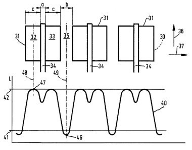
Fig. 2a is a diagrammatic top plan view of an
exposure device as known from the prior art and
comprises a straight row 30 of LED's, each LED 31 being
208 O7 19
provided with a connecting electrode 34 extending in a
direction 36 perpendicular to the row of LED's and
having a width (a) of 5 ~Cm which divides the LED 31 into
two equal parts 32, 33 each having a width (c) of 20 ~,m.
5 Separating zones 35 of a width (b) of 15 ~,m, each time
being formed between neighboring LED's 31, are non-light
emitting. If a photoconductive layer is advanced in a
printer in a direction 36 past the row of LED's, in
order to expose this layer image-wise, the resulting
light distribution in a plane through the main scanning
direction and perpendicular to the plane of the drawing
is as shown in Fig. 2b. In this, the x-axis is shown on
the same scale as that of the row of LED's in Fig. 2a.
Thus, point 47 of the light distribution curve 40 in
Fig. 2b indicates the quantity of light received by a
point on the photosensitive medium if such point is
moved in the auxiliary scanning direction 36 over the
broken line 48 along the row of LED's in Fig. 2a.
Similarly, the quantity of light received by a point on
the photosensitive medium moving past the row of LED's
along the line 49 is denoted by point 46 in the light
distribution curve 40.
The light distribution curve 40 has a maximum (LAX)
in zones straight above the LED's and a minimum (L~~~) in
the zones 35 between the LED's. Since a given quantity
of light is required to expose the photosensitive
medium, L~~~ will have to be at least such as to satisfy
this given quantity.
208 07 19
Line 41 denotes the minimum exposure quantity
required for correct exposure of the photoconductive
layer. Line 42 indicates the maximum permissible
exposure quantity which the photoconductive layer may
reach in those zones which, on movement in the direction
of arrow 36, are taken past the light-emitting zones 32,
33. If the exposure quantity in a zone is higher than
indicated by line 42, then thin lines to be imaged will
no longer be reproduced. The lowest points of curve 40
should be at least above line 41 to allow complete
exposure to the photoconductive layer. In Fig. 2b this
would mean that the total light output has to be
increased, so that parts of the curve 40 will be above
line 42 and thin lines attacked.
Fig. 3a is a diagram showing an exposure device
according to the invention. The reference numerals in
this Figure are the same as those in Fig. 2a. Here the
connecting electrode 34 has a width (a) of 15 ~m of the
separating zone 35. The width of zone (c) is also 15
Vim. The consequence of this is a frequency doubling of
non-emitting zones 34,35, so that a more uniform light
distribution forms at some distance from the LED's, and
hence on the photoconductor. This is indicated by curve
39 in Fig. 3b. Fig. 3b is shown to the same scale as
Fig. 2b and standardized to the maximum exposure just
touching line 42. The bottom edge of the curve 39 is
now situated a light quantity 43 above the background
illumination limit 41. This means that the exposure
7 208 07 19
tolerance has increased. For example, it is possible to
reduce the light quantity of all the LED's to such an
extent that the bottom edge of curve 39 just touches
line 41. The top edge of curve 39 consequently will be
lower than line 42, so that even thinner lines to be
reproduced can be reproduced without difficulty.
It has now been found that a satisfactory
improvement in exposure uniformity occurs if 1.5 > a/b
> 0.75, the optimum being that geometry where a=b.
According to the invention, however, it is also
possible to cover the zone of the connecting electrode
34 with a varnish which does not transmit light so that
no light can emerge at that place. The only factor of
importance for uniformity improvement is the
substantially equal width of the non-emitting zones 34
and 35.
In Fig. 4, the principle as explained with
reference to Fig. 3a-3b is applied differently. The
zones 34 and 35 are again substantially of equal width
(a=b), but now the zones c are much narrower (c ~ 1/3a).
This configuration also gives a satisfactory uniformity
improvement.
Fig. 5 shows an exposure device according to the
invention in which each LED has two separate light-
emitting surfaces 32, 33 which can be energized
simultaneously via a connecting electrode 38. Here
again a = b and a = c.
208 07 19
8
Fig. 6 shows an exposure device according to the
invention in which each LED is divided by connecting
electrode 54 into four light-emitting zones 50, 51, 52
and 53. Here again the zones 55, 56 and 57 have the
same width (a) as the separating zone 35.
The invention being thus described, it will be
obvious that the same may be varied in many ways. Such
variations are not to be regarded as a departure from
the spirit and scope of the invention, and all such
modifications as would be obvious to one skilled in the
art are intended to be included within the scope of the
following claims.