Note: Descriptions are shown in the official language in which they were submitted.
2û8~0~
Apparatus and MPthod for R~ ~nE Harmonic Intelrele~.ce
Generated by a Clock Signal
Field of the Invention
The present invention generally relates to clock siEn~
and more particularly relates to re~ll1~n~ harmonic
intelrelel,ce generated by a ~lock ~iEn
P~k~.o~d ofthe Invention
Co~ ic~t;Qn eqllipme-nt~ of w_ich a radiotelephone
is a cullv~llient ÇY~mp1e, provides an a,u~lo~ul;ate sett;r~ for
1 5 describing the need for the present invçnt;~ n
Radiot~1eph~ne~ generally cu~ l;se audio, logic, and
transce*er ~;lo~ . The logic ~rcuill~ incl~ a processor
that çYecnt~s a sequence of predetermined u~ AI ;nn~,
responsive to the predetel~ued frequency of a lefe,ellce clock
20 sign~1, to control the audio and the transceiver ~lc.~ . A
high frequency clock signal is usually nee-ls-l for the processor
to çYecllte the ~eidl ions at a rate required for typical
radiotelephone operation.
High frequency clock aiEn~1~ are typically characterized
25 by digital square wave pulses with sharp edges that cQnt~in
significant spectral energy. The spectral energy produces
harmonic frequency components, herein~f~er called
harm- nic~, at freql1Pn~ies that are integral multiples of the
frequency of the clock ~ign~1. The harm~ni~ may radiate
30 from lines, call ~h~g the clock ~ign~1, interc~nn?ct;ng the logic
circuitry.
A c~mmon problem in the dssign of r~iotelephones is
that the radiated harmoni~ may interfere with inform~tiQn
ai n~1~ in a b~ndr~ filter in the receiver portion of the
2081 ~O ~
transceiver circuitry. R~ ted harmonics, f~llin~ witLi-l the
frequency bandwidt_ of the receiver's b~n~s filter, ~y
have a power level t~t m~Qlr8 or distorts infqrm~ n ~ n~l~
of lesser power level resulting in poor i..r~ ior. reception.
Tr~ n~l techniques imple~nen~ for re-luçin~
harmonic intelre,ehce include ~hiel~ the receiver circuit~y
from 1 he logic ci~ , p~ the logic ~C~ in a
~ ~diotelephone cavity se~te from the ~e~iver CilC~tl~, and
currents in the .coe;ver chcuiL~ from the logic
~ lth~ ~ these t~hniques provide adequate
solution8, these techniques may require additional parts,
oQ~ ~e valuable engineering development 1ime and
resources, and/or increase the size of the . ~ r~n~, all of
which increase the cost of the r~lioPlepllQn? Furthermore,
in the future, desirable ~m~ller radiotelep~onQ h~ and
higher speed signal proces~inE will increage the MrPlih~Qd
and severity the harmonic inte~relenoe.
For many sit~ n~ of which ~....-..,-.;cation
eq~ Pnt i8 merely an e-~mple, the prior art has not
20 pro~llr~l aI- a~al~s or me~hod for reducing the power level
Of h rmonics, within a predetermined frequency bandwidt_,
generated by a clock ~ignal to solve the problem of h~rmonic
inte. r~l e-,ce while providing for the advantage of lower
eqllipm~r t CoBt~
Summary of the Invention
A device includes a signal generator and a filter. The signal
generator produces a first signal including a fundamental frequency
component and harmonic frequency components having power levels.
The filter filters a second signal over a predetermined frequency
bandwidth to produce a filtered signal. The filtered signal is susceptible
to interference from a harmonic frequency component having a
frequency within the predetermined frequency bandwidth. An apparatus
and method for substantially reducing the interference of the harmonic
frequency component with the filtered signal, comprises a frequency
spreading signal generator and a signal modulator. The frequency
spreading signal generator produces a frequency spreading signal. The
signal modulator modulates the first signal with the frequency spreading
signal to produce a modulated signal including modulated harmonic
frequency components. The power level of a modulated harmonic
frequency component, corresponding to the harmonic frequency
component interfering with the filtered signal, is spread over a frequency
bandwidth greater than the predetermined frequency bandwidth causing
the power level of the modulated harmonic frequency component within
the predetermined frequency bandwidth to decrease, whereby the
interference of the at least one harmonic frequency component with the
filtered signal is substantially reduced.
Brief Description of the Drawings
FIG. 1 shows a block diagram for explaining the cooperative
relationship of the electronic parts of a radiotelephone constructed in
accordance with the teachings and principles of the present invention;
FIG. 2 is an oscillogram plot in the time domain of a frequency
modulated clock signal generated by the clock signal generator of FIG.
1, by way of example and not by way of limitation;
~ 21~ U~ 4
- 3A-
FIG. 3 is a plot in the frequency domain of the clock signal as
shown in FIG. 2, by way of example and not by way of limitation;
FIG. 4 is a plot in the frequency domain of the harmonic, at f3 in
FIG. 3, interfering with a received information signal in the receiver's
bandpass filter of FIG. 1; and
FIG. 5 shows an alternate block diagram for the computer shown
in FIG. 1.
A
~2 ~ 8 11 Q 3~ 4
De~Pile~ De~cription of a Preferred ~.m~iim~t
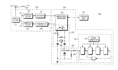
FIG. 1 shows a block diagram for eYpl~ini~ the
coope, dlive relationship of the electronic parts of
5 cv~ ost;-~r eq~ ?~-lt 100, such a~ a portable cellular
~ iot~e~- e, to which the pre~ent i~,ve~lion may he applied.
By way of e ~".~l~, a llet~ile~ description of 1~e electronic
parts used to u~l ~ te the 1 -~iotelep~nne 100 may be found in
an Instruction M~n~ for the Dyna TAC Cellular Portable
10 Telephone, ~t no. 68P81071E5~0, p -hlicl~ed and aV~ip~hlc .
from Motomla 1~ C & E Parts, 1301 E. Algonquin Rd.,
S~hau~hurg,II. 6019~. The~of~eradiotelephone100
may be similar to the design in U.S. Patent No. D315,346 issued on
March 1 2, 1 991, entitled "Portable Radiotelephone or Similar Article".
The radiotelephone generaUy comprises a .. i,~lcr,~
co-.-.. i~on element 101, a l,.~eceive. 103, a co---~ er 105
and a control uDit 107. The wireless ~. .-...~ t;,.. element
101, for e-~mple a conv~ ,;on~1 Q--~ , is co~lple~l to the
transc~ve~ 103 pro~iding a path for i~oi-nq(~ 1R 102
20 coupled th~.~bet..~ The tra~ceivt,. 103 tr~n~mi~e and/or
~ivd8 the ;~-~ol---nl:on ~l~ 102. The co.-.~ 10
controls the trans~;ve~ 103 and/or the control unit 107,
,c~ ive to input aignS~l~ from the same. The control unit
107 provides a-u~er in~e~f~ce for the r~iot~lephone 100. The
25 ~.II,,ol unit 107 may comprise a display, a keypad, an earpiece
and/or a microphone (all not shown).
The transceiver 103 comprises a ~A,~h~ r 109, a
receiver 111, a ~lllpleY filter 113, and l~ndr~Rs filters 114 and
115. The inform~ion si~ 102 are coupled to the duplex
30 filter 113 via the ~ntenn~ 101. The duplex filter 113 separates -
the receive and transmit f~equency bandwidths such that a
information signal at line 117 may be received at the same
time another inform~tion signal at line 119 is transmitted.
The inform~t;on ~i~n~l, at ~ine 117, is coupled to the ,eceive
. .
,.
53 Z~8~ ~ 4
111 via a h~n~lrs~s filter 115, having a relatively narrow
pre~lnte-minQ-l band of freqllen~ies at w_ich the ~ 111 is
~igne~l to operate while reject;ng all other freqll~ncies.
I~kewise, the informs~ n ~gn~l, at line 119, is co~lple l to t_e
tr~n~.. ;l,le~ 109 via a h~n~r~ss filter 114, having a relatively
narrow predetermined band of freql~ at which the
transmitter 109 is ~Qsi~ned to operate wile rejec1;nE ~11 other
frequencies.
The cc~ er 105 generally c~ es a clock signal
10 generator 123, an audia/logic l,.oce~or 121, a psel~lorandom
noi~e signal generator 127, and a frequen~ mo~ s~r 125.
The ~lock 8ig~1al generator 123 ~ , ~?~ a ~~ ,Qn~l
oR~illgt~r 129, guch as a crystal osmlls-tor~ and ~ s-~e~ bia~
w~ . The clock signal generator 123 pro~ es a clock
15 ~ignsl, l~v~ a pre~i- lc. ~..i..9tl frequency, at line 131. The
clock sign~l at line 131 is a laf~ ce signal that provides the
timing for the audio/ logic ~locPRsor 121.
The audio/logic processor 121, for r ~ Jle a digital
signal processor (DSP), c~ l,.;Re8 me~nR for eyemltir~ a
20 sequence of predetermined oyel~lions (otherwiRe known as a
l,r~la.a)"e*l~-.~ive to t~e pre-lete....;..e, i frequency of the
clock signal at line 131. By way of ç~ e, the DSP may be a
DSP/56001, ~lescrihe~l in DSP/56001 Digital Sign~ oeeR,R~or
User M~nll~ revision 1, av~it~ble fromMotorola Inc. The
25 frequency of the clock signal at line 131, for ~ e 8 MHz, is
such that the operations may be çYec~ l at a rate lequued for
t~rpical o~el~.lion of the r~-liot~leph-n~ 100. The ~lock signal at
line 131 may be characterized by digital square wave pulse~
with 6harp edges that contain significant spectral energy
30 producing the aforementioned harmonics.
The pseudor~n-lom noise generator 127 produces a
frequency spre~ling signal at line 130 that is a deterrniniF~ic~
periodic signal and appears to have the st~P~;c~l properties of
white noise. A detailed description of pseudorandom noise
- 6
generators may be found in ~Digital CQ~--.-..;cations,
n~l~mants.1R and App1ir~ n~~ by Bernard Sklar, Chapter
10, ~)1988, pnhli~hsA by Pr_ntice Hall.
The frequency spre~li~ signal at line 130 is cl!mhineA
5 with an input to the clock signal ~e~e~a~or at line 132 via the
frequency moA~ tor 12~. A Aet~i1eA ~l?r~pt;~n of the
frequency mnAl11~tor may be found in ~Solid State Radio
F~n~",~ by Herbert L. Rrauss, Ch~rleE W. Bostian and
Fre~e~ir~ H. Rabe, Chapt._r 15, pp. 483485, ~ 1980, pllhli~hgA --
10 by Jo_n W~ey and Sons, Inc.
By frequency mn~ h~ the input to the ~lo~k signalgenerator at line 132 with the frequency spre~ling signal at
line 130, the power of the h~. ..-onics are spread over a
frequency bandwidth, greater than the pre~ ~te~
15 frequency bandwidth of the ,ac~ve~ts b~qn~ 3 filter whereby
the power level of a h~ ~o ~;c p~44eA t~rough tlle bandwidth of
the ,eceiver~s b~9n~lr~c~ filter, i8 reAllce~l The power level of
the h~rmf niC, filtered by the ~ 8 b~n~lr~fi filter 115, is
re~n~e~ 80 as not to ~sk or distort a received ;..~
20 signalatline117. Theresult~rields. l.L~ed~ lionofthe
le -e;ved illfo~ JdQ n signal at line 117, without using the
afole...~nt;oned traditional te~hniques for re~v~i~ harmonic
intelfe~ ce, while providing for the adv~tage 4f lower
eqllipment cost.
A cullva~ent ~nh~n~ r~t to the rr~liot~er~- ? 100 of
FIG. 1 i8 to replace a signal generator 133 in t_e
psel~clor~nllQm noise signal generator 127 using a binary
division of the clock signal at line 131. Thus, only a single
signal generator, i.e. the clock signal generator 123, is needed
to generate both the lafelellce clock signal at line 131 and the -
~equency spreading signal at line 1 30.
FIG. 2 i8 an oscillogram plot in the time ~om~qin of the
frequency modulated clock signal at line 131 generated by the
clock signal generator 123 of FIG. 1, by way of eY~mple and not
7 ~ ~
by way of li~ila~,io~ The plot shows fo~lr pulses 201-204 of the
clock signal at line 131. Each pulse has a rising and a f~llin~
edge, 205 and 207, respecl;vely, on pulse 201 for çY~mple. The
rising and f~ E edges of each pulse 202-204 are spread over
5 time. By way of eY~mple, 1.5 ~7 deviation m~lnl~ on the 8
MHz clock signal CO~ to 190 ppm of jitter on the clock
signal at line 131. This ~n~ollnt of jitter is sllffiriP.nt for
re-lll~n~ the power ~h~l density of the h~ nic~ without
sllhEt~nt;~lly ~ ;.,E the ~;min~ of the audio/logic processor
10 121. FIG. 2 shows 1~e a~ouut of jitter increasing for pulses
201~hrough204. Increa~ingu~c~ ofedgeloc~ nis
due to increasing ac~m~ Q~l of jitt_r with increasing
A~4.~ n of time from the le~ E edge of t_e ~eÇelence
pulse 205.
FIG. 3 iB a plot in t_e frequency ~lr~in of the clock
signal at line 131 as shown in FIG. 2, by way of eY,qmrle and
notbywayofl;..~ n TheclocksiEn~latline131h~a
filn~3~m~n~l frequency, fo, and harmonic% fi, f2 and f3. The
solid and dotted lines, corresrQn~inE to fo-f3, represent the plot
in the frequency ~ n~in of t_e clock signal at line 131 before
and after being mo~ te~ r~specl;vely, by the frequency
spre~in{~ signal at line 130. The effect of m~nl~tinE the clock
sigDal at line 131 with the frequency spr~a~dinE signal at line
130 is that the fitn~l~man~l frequency fo of the <~lock signal and
its h~t~n~ nics fi-f3 are spread over the plurality of frequencies,
i.e. a bandwidth wider than the predetérmine~l bandwidth of
the receive~-'s b~ndr~ss filter, such that the power spectral
density of any one harmonic, within the b~n~r~Rs filter 115, is
reduced.
The power of the modulated harmonic rçm~in~ equal to
the power of the llnmo~ulated harmonic such that the total
power of the harmonic is conserved. As the frequency of the'
harmonics increase, the spectral spre~tling of the modulated
harmonic as a percentage of the unmodulated harmonic
.q= .
8 20XI~
bandwidth increases. Thus, for _igher order h~rmonics the
power spectral density reclvct;or of the m~~ te 1 harmonic
as a ~elc~-t~é of the llnmo~ tecl h~rmQnic iB greater than
for lower order harmgnicR.
FIG. 4 is a plot in the frequency ~om~in of the receivel-'s
h~nllpA~s filter 116 and the llnmoA~ t~l harmonic 301 at f3
int~.rt~ g with a leccived ~rol~ t;~n signal 302 at line 117.
The ~ceiver's b~n~lr~s filter 115 occllpies a frequency
bandwidth from f4 to fs, for ay~mple 10 KHz. The power
~e.,l,ldl density of the Ri~l~, within the b~n~lr~ filter 115,
is represçnte~l by the area underneath the curves,
repreBçn*ng~i~n~lR301-303, be~wee~ freqllencies f4 and fs.
The llnmo~ t~ harmonic 301 has a power ~l,ecll~l
density at f3,--within the b~n~lp~ filter 115, that masks the
power spectral density of the leceived inform~t;o-l signal 302
from the lecciver 111. By frequency mo~ t;nE the clock
signal at line 131, the power spectral density of t_e
~nmo~ l h~rmonic 301 is spread over a plurality of
freqllancic~ in the frequency bandwidth between f6 and f7. The
effect of such ~ecll al spre~ is that the power of the
~nm~lul~terl harmonic 301, intercepted by the bandwidth of
the bAn~lp~Rs filter 115, is re~lllcerl to a power level, repregçnt~l
by the modulated h~rmnnic 303, below the power level of the
rec~ived inform~t;on signal 302. ConRequently, the le~ived
inform~t;on signal 302 can now be rlPte~te~ by the receiv~r 111.
After the spre~ g the power of the lmmo~ulated
harmonic 301, the frequency bandwidth belween f6 and f7 of the
modulated harmonic 303 is subst~nt;~lly greater than the
frequency bandwidth between f4 and fs of the receivel's
h~n~r~cs filter 115. Thus, the power spectral density of the
h~.,ll,l.ic within the b~n~lr~ss filter 115 is gnh~t~nt;~lly
reduced. A power level re~ n of a mot~ harmonic
relative to an nnmo~ te l harm-nic, Wit~ill a predetermined
frequency bandwidth, may be represçnts~3 by:
~ ,i
9 ~ &
Power (dB) ~ 10 log ~2WxJ
where n is the order of the harmonic, x is the amount of
5 modulation and W is the bandwidth of the ban~r~ss filter
115. By way of example, a 100th order harmonic having
1.5 KHz modulation provides 14.77 dB power re~uetion,
relative to an unmodulated 100th order harmonic, within
a ban~ ss filter having a 10 KHz bandwWth.
FIG. 5 shows an ~ltern~te block dia~-~ for the
co~ ,~r 105 shown in EIG. 1, constructed in accordance with
the teachings and principles of the l les~nt ~ o n A
co~lve~ l phase ~ tor 501 is used as ~e means for
co-nh;ni~ the frequen~r spre~ signal at line 1 30and the
15 nnmof~ t~ clock signal atline 503. Aphase mo~ te 1
clo~k signal at line 505 provides the timiDg for the audia/logic
processor 121. Thus, the dock signal is phase mo~ t~ in
FIG. 5 to reduce the power spectral density of a harm~-ic,
within the le&;vel's h~n~p~ filter 115, 6~l~ted by the
20 clock sigDal generator 123. A fletsile~ dee_;y1;on of
conve~ n~l phase modul~tors may be found in ~Solid State
Radio h~r~ineeringn by Herbert L. Krauss, Charles W. Bostian
and Fre leriC~ H. Rabe, Cl~y1~l- 15, pp. 485 486, ~1980,
pllhlis:he~ by John ~ley and Sons, Inc.
. .~ ,