Note: Descriptions are shown in the official language in which they were submitted.
2~8123~
MOTION COMPENSATION ENCODING OF A PICTURE INPUT SIGNAL
INTO A PICTURE OUTPUT SIGNAL OF A PREDETERMINED BIT RAT~
BACKGROUND OF TH~ INVENTION:
This invention relates to a picture signal
encoding device which is a block matching type motion
compensation encoding device and which is for encoding a
picture input signal into a picture output signal.
The input signal is typically a video signal of a
television signal and represents a succession of pictures
in successive periods which recur at a predetermined
period, such as a ~rame period, so that each of the
successive periods is equal to the predetermined period.
The output signal represents the pictures with a
predetermined bit rate. Each of the pictures has a
movable part movable between a current picture
represented by the input signal during a current period
of the successive periods and a previous picture
represented by the input~signal during a previous period
which is one predetermined period prior among the
successive periods to the current period.
Although referred to as a part, the movable part
may extend to a whole area of each picture. The movable
part need not be different between two consecutive ones
of the pictures. It is possible to divide or partition
,
..
2~8~3
each picture into a plurality of blocks, each consisting
of, for example, seven picture elements (pels) in each of
seven consecutive horizontal lines.
A block matching type motion compensation
encoding device is disclosed in Japanese Patent
Prepublication (Kôkai) No. 158,784 of 1980 for an
invention by Akira Hirano filed on May 28, 1979, in Japan
under Patent Application No. 65,853 of 1979. Another
~lock matching t~pe motion compensation encoding device
is described in the Japanese language in an article
contributed by Toshio Koga and three others including the
above-named Hirano and the present inventor under the
title of "Kaigi Terebi Singô no Ugoki Hosyô Hurêmukan
Hugôka (Motion-Compensated Interframe Coding for Video
Conference)" to "Tûsin Hosiki Kenkyûkai Siryô
(Communication System Study Group Pamphlet)", CS81-37,
pages 85 to 90, published July 22, 1981, by the Institute
of Electronics and Communication Enginee~s of Japan.
Still another block machining type motion compensation
encoding device is described in a paper submitted by T.
Koga and four others to IEEE International Conference on
Communications, June 19~22, 1983, under the title of "A
1.5 Mb/s InterframP Codec with Motion Compensation"
(numbered 83CH1874.7/83/0000.1161). The encoding devices
of the Koga ~t al article and paper are ~ubstantially
identical insofar as the instant invention is concerned.
Each will be called a Koga et al encoding device.
~8~233
In the manner which will later become clear, the
Koga et al encodin~ device comprises a vector detector.
Supplied with the picture input signal, the vector
detector detects displacements as motion vectors in the
movable part. Detecting the motion vectors, the vector
detector produces a motion vector signal representative
of the motion vectors.
Supplied with the picture input signal and a
subtracter input signal which will presently be
described, a subtracter calculates a signal difference
between the picture input signal and the subtracter input
signal to produce a difference signal representative of
the difference. A forward quantizer quantizes the
difference signal into a quantized signal. A backward
quantizer dequantizes the quantized signal into a
dequantized signal. An encoder encodes the motion vector
signal and the quantized signal into the picture output
signal.
Supplied with the dequan~ized signal and an adder
input signal which will shortly be described, an adder
produces a sum signal representative of a signal sum of
the dequantized signal and the adder input signal. A
motion compensation predictor subjects th~ motion vector
signal and the sum signal on a block-by-block basis to
block match between the current and the previous
pictures. Carrying out the block match, the motion
compensation predictor predicts the picture input signal
with motion compensation and with error minimization to
2~gl~33
produce a predicted input signal which is referred to as
an optimum prediction signal in the Koga et al paper and
is used as the adder input signal. The sum signal serves
as a local decoded signal into which the dequantized
signal is decoded.
As a consequence, a combination of the adder and
the motion compensation predictor serves as a decoding
and motion co~pensating circuit for subjecting the motion
vector signal and the dequantized signal to the block
match to produce the predicted input signal. A predicted
signal supply connection supplies the predicted input
signal to the subtracter as the subtracter input signal.
The subtracter therefore produces the difference signal
as a prediction error signal representative of the
difference as a prediction error.
It is now understood that a whole combination of
the subtracter, the forward and the backward quantizers,
the decoding and motion compensating circuit, and the
predicted signal suppl~v connection serves as a predictive
quantizing arrangement for producing the predicted input
signal with the motion vector signal used to carry out
the block match with the motion compensation and with the
error minimization in producing the prediction error
signal representative of the signal difference between
the picture input signal and the predictive input signal.
Furthermore, the predictive quantizing arrangement
quantizes the prediction error signal into the quantized
signal.
2~8~3
More briefly, the predictive quantizing
arrangement derives the prediction error signal from the
picture input signal and the motion vector signal and
quantizes the prediction error signal into the quantized
signal.
With a compact size of about 48 ~ 45 x 45 cm, the
Koga et al encoding device is excellently operable when
the predetermined bit rate is 1.544 Mb/s. A considerable
amount of encoded information, however, still remains in
the picture output signal.
As a result, it is difficult with the Koga et al
encoding device to select a slower bit rate of, for
instance 64 bit~s, as the predetermined bit rate even
when the picture output signal is subsampled.
Furthermore r the picture output signal must use an
appreciably much amount of the encoded information when
the movable part has a wide area. In such an event, the
forward quantizer must quantize the error signal with a
coarse quantization step. Alternatively, encoding of the
picture input signal must intermittently be suspended.
This gives an objectionable picture quality to pictures
reproduced from the picture output signal. Inasmuch as
such a slow bit rate is a problem to be solved by tAis
invention, the slower bit rate will herein be referred to
afresh as the predetermined bit rate.
SUMMARY OF THE INVENTION:
It is consequently an object of the present
invention to provide a picture signal encoding device
which is a block matching type motion compensation
encoding device and is capable of encoding a picture
input signal into a picture output signal representative
of a small amount of encoded information.
It is another object of this invention to provide
a picture signal encoding device which is of the type
described and which encodes the picture input signal into
the picture output signal of a predetermined bit rate.
Other objects of th.is invention will become clear
as the description proceeds.
On setting forth the gist of this invention, it
~ is possible to understand that a picture signal encoding
device is operable as a block matching type motion
compensation encoding device including an encoder for
encoding into a picture output signal a quantized signal
in addition to a motion vector signal representative of a
displacement of a movable part between two of a plurality
of pictures which are represented by a picture input
signal in successive periods recurring at a predetermined
period-
According to this invention, the above-understood
picture signal encoding device comprises~
controllable predictive quantizing means for controllably
quantizing into the quantized signal a prediction error
signal derived from the picture input signal and the
motion vector signal; (~) a controller for producing a
control signal indicative of a predetermined value
substantially in each of preselected periods of the
~0~233
successive periods; and (C) control signal supply means
for supplying the control signal to the controllable
predictive ~uantizing means to make the controllable
predictive quantizing means produce the quantized signal
by substituting a zero signal for the error signal when
the control signal indicates the predetermined value.
In the above-described gist of this invention,
each of the preselected periods may appear once in an
int~gral multiple of the predetermined period.
Preferably, the zero signal should not be substituted for
the prediction error signal in each duration in which the
motion vector signal of each of the preselected periods
represents the motion vectors having magnitudes which are
equal to or greater than a preselected threshold value.
It is possible to use as the duration an interval of time
during which the prediction error signal has an error
absolute value which is equal to or greater than a
preselected threshold value. Alternatively, the duration
may be an interval of time during which the motion
vectors are not identical with a representative vector
which is used in place of most of the motion vectors that
have a common direction with sense. As a further
alternative, each duration may be an interval of time
during which current vectors of the motion vectors of the
current picture have a correlation value relative to
previous vectors corresponding to the current vectors in
the motion vectors of the previous picture when the ~ero
signal is substituted for the prediction error signal
~gl~3~
produced in connection with the current picture and
furthermore when the correlation value is less than a
preselected threshold value.
BRIEF DESCRIPTION OF THE DRAWING:
Fig. 1 is a block diagram of a picture signal
encoding device according to a first embodiment of the
instant inventioni
Fig. 2 exemplifies a movable part in two
consecutive pictures;
Fig. 3 is a diagram for use in describing a
motion vector;
Fig. 4 shows motion vectors representative of
displacements of the movable parts exemplified in Fig. 2;
Fig. 5 is a time chart for use in describing
operation of the picture signal encoding device
illustrated in Fig. l;
Fig. 6 is a block diagram of a controller for use
in the picture signal encoding device depicted in Fig. l;
Fig. 7 is a time chart for use in describing
operation of the con~roller illustrated in Fig. 6;
Fig. 8 is another time chart for use in
describing operation of the controller shown in Fig. 6;
Fig. 9 is a flow chart for use in describing a
controller which is for use in the picture signal
encoding device depicted in Fig. l;
Fig. 10 is a time chart for use in describing
operation of the controller operable in accordance with
the flow chart shown in Fig. 9;
2Q~2~
Fig. 11 is a block diagram of a picture signal
encoding device according to a modification of the
picture signal encoding device depicted in Fig. l;
Fig. 12 is a block diagram of a picture signal
encoding device according to a second embodiment of this
invention;
Fig. 13 is a block diagram of a controller for
use in the picture signal encoding device depicted in
Fig. 12;
Fig. 14 is a time chart for use in describing
operation of the controller illustrated in Fig. 13;
Fig. 15 is another time chart for use in
describing operation of the controller shown in Fig. 13;
Fig. 16 is a flow chart for a controller for use
in the picture signal encoding device depicted in Fig. 12;
Fig. 17 is a time chart for use in describing
operation of the controller operable in compliance with
Fig O 16;
Fig. 18 is a block diagram of a picture signal
encoding device according to a modification of the
picture signal encoding device illustrated in Fig. 12;
Fig. l9 is a block diagram of a picture signal
encoding device according to a third embodiment of this
invention;
Fig. 20 is a time char~ for use in describing
operation of a controller which is for use in the picture
signal encoding device illustrated in Fig. l9;
2 ~ 3 3
Fig. 21 is a block diagram of a picture signal
encoding device according to a fourth embodiment of this
invention;
Fig. 22 shows a velocity component plane for use
in describing operation of the picture signal encoding
device illustrated in Fig. 21;
Fig. 23 is a block diagram of a controller for
use in the picture signal encoding device depicted in
Fig. 21;
Fig. 24 shows a part of a flow chart for use in
describing operation of a controller which is for use in
the picture signal encoding device depicted in Flg. 21;
Fig. 25 is a time chart for use in describing
operation of the controller illustrated in Fig. 23;
Fig. 26 is a block diagram of a picture signal
encoding device according to a fifth embodiment of this
invention;
Fig. 27 shows a current picture for use in
describing operation of the picture signal encoding
device illustrated in Fig. 26; and
Fig. 28 is a time chart for use in describing
operation of a controller which is for use in the pic~ure
signal encoding device depicted in Fig. 26.
DESCRIPTION OF THE PREFERRED EMBODIMENT5:
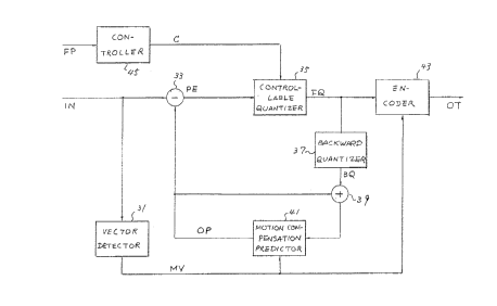
Referring to Fig. 1, the description will begin
with a picture signal encoding device according to a
first embodiment of the present invention. The picture
siynal encoding device is a block matching type motion
~0~2~3
lJ
compensation encoding device of the t~pe described
heretobefore in connection with the Koga et al article
and paper and is for encoding a picture input signal into
a picture output signal.
S In the manner described hereinabove, the input
signal represents a succession of pictures in successive
periods which recur at a predetermined period, such as a
frame period of a television signal, so that each of the
successive periods is equal to the predetermined period.
10 The output signal represents the pictures with a
predetermined bit rate.
It will be assumed that the picture input signal
is a video signal of a television signal. Each of the
pictures has a mova~le part movable between a current
picture represented by the input signal during a current
frame F of the successive frames and a previous picture
represented by the input signal during a previous frame
F' which is one frame period prior among the successive
frames to the current frame.
Although re~erred to as a part, the movable part
may be a whole area of each picture. The movable part
need not be different be~ween two consecutive pictures.
It is possible to divide or partition each picture into a
plurality of blocks, each consisting of, ~or example,
seven picture elements (pels) in each of seven
consecutive horizontal lines.
In Fig. 1, the picture signal is indicated by IN
and is supplied to a vector detector 31. In the manner
~8~3t~
known in the art, the vector detector 31 detects motion
vectors or displacements in each picture and produces a
motion vector signal MV representative of the motion
vectors. The vector detector 31 produces the motion
vector signal by subjecting the picture input signal to
block match in the manner described below. Alternative-
ly, the vector detector 31 may detect the motion vectors
with reference to each pair of picture elements which
correspond in the current and the previous pictures with
the displacement taken into consideration.
Turning to Fig. 2 during a short while, the
current picture shows an upper body of a man as outlined
by a dashed line. It will be surmised that the upper
body was represented in the previous picture as shown by
a solid-line outline. The upper body is the above-
mentioned movable part.
Further turning to Fig~ 3, the current frame or
picture is depicted at F and the previous frame or
picture, at F', along a time axis t. One of the
above-mentioned blocks is shown as a current block A in
the current frame by a small rectangle. It will be
presumed that this part of the current picture was
present in the previous picture as a previous part A'~ A
current point is taken into consideration in the current
block of the current picture. Another point corresponds
in position to the current point as a corresponding point
in the previous picture. It will be presumed that the
current point has moved ~rom a previous point in the
2~8~33
13
previous part. A displacement between the previous and
the current points represents a motion vector V of the
current point or of the current block.
It is known in the art to find on a block-by-
block basis a previous block that has moved to thecurrent block. For this purpose, the previous picture is
stored block by block in a frame memory (not shown) as
stored blocks. The current block is selected in the
current picture. The previous block is given by one of
the stored blocks that has a highest correlation to the
current block. The correlation is calculated by a total
sum of either squares of differences between correspond-
ing picture elements in the current block and in each of
the stored blocks or of absolute values of the
differences.
5till further turning to Fig. 4, the motion
vectors are exemplified, one in connection with each
block. In the example being illustrated, most of the
motion vectors have a common magnitude and a common
direction wi~h sense~
Turning back to Fig. l, a subtracter 33 is
supplied with the picture input signal IN and a
subtracter input signal OP which will presently be
described. The subtracter 33 produces a difference
signal PE which represents a signal di~ference between
the picture input signal and the subtracter input signal
and will shortly become clear.
2~23.~
14
A forward quantizer 35 is a controllable
quantizer in Fig. 1. As ~ill become clear as the
description proceeds, the controllable quantizer 35
controllably quantizes the difference signal into a
quantized signal FQ with a forward quantizing
characteristic which is given preferably by nonlinear
step sizesO A backward quantizer 37 dequantizes the
quantized signal into a dequantized signal BQ with a
backward quantizing characteristic which is complementary
to the forward quantizing characteristic. Supplied with
the dequantized signal and an adder input signal which
will soon be described, an adder 39 produces a sum signal
which represents a signal sum of the dequantized and the
adder input signals and is a local decoded signal into
which the dequantized signal is decoded.
A motion compensation predictor 41 i5 discussed
in detail in the afore-referenced Koga et al article and
paper as a single variable delay circuit and a
combination of a frame memory and a variable delay
circuit. A little more in detail, the motion
compensation predictor 41 subjects the motion vector
signal MV on the block~-by-block basis to block match
between the current and the previous pictures. Carrying
out the block match, the motion compensation predictor ~1
predicts the picture input signal from the sum signal
with motion compensation and with error minimization to
produce a predicted input signal OP, which is referred to
as an optimum prediction signal in the Koga et al paper.
2 ~ 3 3
Together with the vector detector 31, the motion
compensation predictor 41 is described more in detail in
the above-cited Japanese Patent Prepublication.
A connection between the adder 39 and the motion
compensation predictor 41 supplies the predicted input
signal to the adder 39 as the adder input signal.
Another connection between the subtracter 31 and the
motion compensation predictor 41 serves as a predicted
signal supply arrangement for supplying the predicted
input signal to the subtracter 33 as the subtracter input
signal. The subtracter 33 therefore produces as the
difference signal a prediction error signal PE
representative of a prediction error.
A combination o~ the adder 39 and the motion
compensation predictor 41 serves as a decoding and motion
compensating circuit for subjecting the motion vector
signal to the block match. Carrying out the block match,
the decoding and motion compensating circuit uses the
dequantized signal in producing the decoded signal for
use therein and the predicted input signal for use by the
subtracter 33 as the subtracter input signal.
- A whole combination of the subtracter 33, the
controllable and the backwaxd quantizers 35 and 37, the
decoding and motion compensating circuit (39, 41), and
the predicted signal supply arrangement serves as a
controllable predictive quantizing arrangement for
controllably quantizing the predicted input signal into
~he quantized signal. It should be noted in this
3 ~
16
conne~tion that the predictive quantizing arrangement
(33, 35, 37, 39, 41) derives the prediction error signal
from the picture input signal and the motion vector
signal on controllably quantizing the motion vector
signal into the quantized signal.
An encoder 43 is preferably a variable length
encoder for encoding the motion vector signal and the
quantized signal into a picture output signal OT
representative of the pictures with a predetermined bit
rate which is considerably lower than that attained b~ a
conventional picture encoding device and is as low as 64
kb/s. More particularly, the encoder 43 encodes the
motion vector signal into vector representing codes and
the quantized signal into error representing codes to
produce the vector and the error representing codes
collectively as the picture output signal. Huffman codes
are preferably used as the vector and the error
representing codes. The low bit rate is achieved in the
manner described in the following.
2~ Supplied with frame pulses FP indicative of
partitions of the frame periods in the video signal, a
controller 45 produces a control signal C indicative of a
predetermined value in each o~ preselected periods of the
successive periods. In Fig. 1, each preselected period
appears in an integral multiple o~ the predetermined
period. In other words, the control signal is given the
predetermined value once in the integral multiple of the
frame period, such as two or three frame periods.
2~8~ 233
A connection between the controllable quantizer
35 and the controller 45 serves as a control signal
supply arrangement for supplying the control signal to
the controllable quantizer 35. Controlled by the control
signal C, the controllable predictive quantizing
arrangement quantizes the picture input signal IN into
the quantized signal FQ with a zero signal substituted
for the prediction error signal PE whenever the control
signal indicates the predetermined value. The
controllable quantizer 35 quantizes the zero signal into
a zero representing code. As a consequence, the encoder
43 produces the vector and the zero representing codes
collectively as the picture output signal when the
control signal indicates the predetermined value. When
the encoder 43 is a run length encoder, the zero
representing codes are encoded into run length codes.
It is therefore possible to implement the
controllable quantizer 35 by a quantizer read~only memory
which may be accessed by an address signal composed of a
most significant bit and less significant bit. The
control signal C is used as the most significant bit with
a binary zero value used as the predetermined value and
with a binary one value used as a different value of the
control signal. The less significant bits are
representative of the prediction error represented by the
prediction error signal PE. A zero value is
preliminarily stored in memory addresses which are
accessed when the address signal indicates the binary
- , . ' : -
:
. ,' ,
233
18
zero value as the most significant bit. Quantized values
are preliminarily stored in remaining addresses accessed
by the less significant bits of the address signal.
Referring to Fig. 5, zeroth through third frame
pulses are depicted along an upper row labelled FP.
These frame pulses define zeroth through third frame
periods tO, tl, t2, and t3. It will be assumed that the
integral multiple is equal to two. In this event, the
control signal indicates the binary zero value as the
predetermined value during the first and the third frame
periods and the binary one value as the different value
in other frame periods.
Turning to Fig. 6, the controller 45 is
implemented by a shift register 47 which is, for example,
a parallel access shift register SN74LSl95 manufactured
and sold by Texas Instruments and is stepped by build-up
edges of the frame pulses FP which are supplied to a
clock terminal CLX for use as clock pulses. First
through ~ourth input signals A, B, C, a~d D are supplied
in parallel to first through fourth signal input
terminals IA, IB, IC, and XD. First ~and second binary
zero signals are supplied to true and inverse input
terminals J and /K. A binary one signal is supplied to a
clear terminal CLR. A shift/load signal is supplied to a
shift/load terminal S/L. The shift register 47 has first
through fourth signal output terminals QA, QB, QC, and QD
and produces a shift register output signal from the
fourth signal output terminal QD to supply the register
~ - ' , -
2~1233
19
output signal to the shift/load terminal as the
shift/load signal.
When the shift-load signal indicates the binary
~ero value and the binary one value, the shift register
47 is operable in a parallel access mode and in a serial
shift mode of operation. If the integral multiple is
equal to two, each of the first through the third input
signals A to C is given the binary zero value and the
fourth input signal D, the binary one value. In the
parallel access mode, the shift register 47 is loaded
with the first through the fourth input signals at each
build-up edge of the frame pulses and produces the first
through the fourth input signals at the first through the
fourth signal output terminals as they are. The shift
register 47 is therefore put in the serial shift mode of
shifting the first binary zero signal and an inversion of
a signal supplied through the inverse input terminal to
the first signal output terminals and the first through
the third input signals to the second through the fourth
signal output terminals. The shift register 47 is
- consequently put back into the parallel access mode at
the build-up edge that next follows the build-up edge
under consideration.
Further turning to Fig. 7 with reference to Fig.
6 continued, the frame pulses are illustrated along a
first or top row labelled FP. The shift register 47
produces first through fourth output signals at the first
through the fourth signal output terminals QA to QD in
.~ . ,
., -
2V~2~
the manner depicted along second through fifth or bottom
rows labelled QA, QB, QC, and QD. The fourth output
signal is the shift register output signal and is used as
the control signal C in the picture signal encoding
device illustrated with reference to Fig. l.
Referring to Fig. 8 with Fig. 6 again referred
to, it will now be assumed that the integral multiple is
equal to three. In this event, each of the first and the
second input signals is given the binary zero value and
each of the third and the fourth input signals, the
binary one value. The frame pulses are illustrated along
a first or top row labelled FP. The first through the
fourth output signals are depicted along second through
fifth rows labelled Q~ through QD. $he shift register 47
is put into the serial shift mode at the build-up edge of
the zeroth frame pulse, into the parallel access mode at
the build-up edge of the first frame pulse, into the
serial shift mode at the build-up edge of each of the
second and the third frame pulses, and in the parallel
access mode at the build-up edge of a next frame pulse.
It is now understood with reference to Figs. 6
through 8 that the integral multiple can be given A
desired value by varying the first through the fourth
input signals to which the binar~ one value is given and
2S by adding fifth or other input signals if necessary. In
any event, the greatest numbered output signal is used as
the control signal in the picture signal encoding device
of Fig. l. The integral multiple should, however, be as
2 ~
21
small as possible in order to reduce an amount of encoded
information which is carried by the picture output
signal.
Summarizing, the parallel access shift register
47 is supplied with the frame pulses FP and with the
first through the fourth input signals A to D as a
plurality of register input signals which are
collectively indicative of the integral multipleO
Supplied with the frame pulses as clock pulses and with
the register input signals, the shift register 47
produces the control signal C indicative of the binary
zero value as the predetermined value and the binary one
value as the different value other than or different from
the predetermined value, one at a time.
Referring to Fig. 9 in addition to Fig. 1 and
Fig. 6 or 8, the controller 45 is alternatively
implemented by a processor, such as a microprocessor,
programmed as follows. At a first step Sl.l, the
integral multiple is set as an initial condition in the
processor as indicated by "set N", where N represents the
integral multiple. At a second step S1.2, the processor
repeatedly detects the build-up edge (EDG) of each of the
frame pulses FP supplied thereto. At a third step S1.3,
the processor calculates an integer difference a which is
equal to the integral multiple minus one. At a fourth
step Sl.4, the processor checks whether or not the
- difference i9 equal to zero. If the difference is equal
to zero, the processor produces at a first step Sl.5 a
2 ~ ~
processor output signal as the control signal with the
binary zero value, namely, with the predetermined value.
If the difference is not equal to zero, the processor
produces the processor output signal at a sixth step Sl.6
with the binary one value. The fifth and the sixth step
return to the first step Sl.l in preparation for
production of the control signal with regard to the
pictures of another sequence of the successive periods.
The build-up edge is a leading edge when called more in
general.
Turning to Fig. 10 with Figs. 1 and 9 admittedly
referred to, it is again assumed that the integral
multiple is equal to two and that the initial condition
is set in the controller 45 prior to the zeroth frame
pulse of the frame pulses illustrated along a first or
top row labelled FP. The integer difference is shown
along a second or middle row labelled ~. The control
signal is depicted along a third or bottom row labelled
C.
When Fig. 10 is compared with Fig~ 8, the control
signal C has an opposite polarity. This, however,
introduces no problem.
Referring to Fig. 11, the description will
proceed to a picture signal encoding device according to
a modification of the device illustrated with re~erence
to Fig. 1. Similar parts are designated by like
reference numerals and are similarly operable with
likewise named signals which are indicated by like
2~gJ 2~ r~
23
reference symbols.
The controllable predictive quantizing
arrangement comprises a selector 49 between the
subtracter 33 and the forward quantizer 35 which is not
controllable in the example being illustrated. Supplied
with the control signal C, the selector 49 selects a zero
signal "0" and the prediction error signal PE as a
selected signal for supply to the forward ~uantizer 35
when the control signal indicates the predetermined value
and otherwise, respectively. The forward quantizer 35
quantizes the selected signal into the quantized signal
FQ.
It is alternatively possible to place a selector
49' on an output side of the forward quantizer 35 in the
manner illustrated by a dashed-line block. The forward
quantizer 35 will be said to produce a quantizer output
signal. Controlled by the control signal C, the selector
49' selects the zero signal "0" and the quantizer output
signal as the quantized signal FQ when the control signal
indicates the predetermined value and otherwise.
Reviewing Figs~ 1 through 11, it has been found
by the inventor that the picture output signal OT
represents the pictures with an objectionable ~uality
when the zero signal is substituted for the prediction
error si~nal PE derived from the motion vector signal MV
representative of rotation of the movable part. This is
the case when the movable part is subjected to the
displacement of a great magnitudeO
2 3 ~
2~
Referring now to Fig. 12, attention will be
directed to ~ picture signal encoding device according to
a second embodiment of this invention. Similar parts are
designated by like reference numerals and are similarly
operable with likewise named signals which are designated
by like reference symbols. The motion vector signal MV
is used in controlling the controller 45.
Refexring to Fig. 13 with Fig. 12 continuously
referred to, the controller 45 comprises either the shift
register 47 illustrated with reference to Fig. 6 or the
processor described with reference to Fig. 9. It should
be understood that the processor is depicted as the shift
register 47 in Fig. 130 Either the shift register output
signal or the processor output signal will now be called
a controller internal signal.
A controller read-only me~ory (ROM) 51 is
supplied with the motion vector signal MV as an address
signal to produce a memory output signal. Supplied with
the controller internal signal and the memory output
signal, an OR gate 53 produces the control signal C. A
preselected threshold value K is preselected in
connection with magnitudes of the motion vectors
represented by the motion vector signal. The threshold
value is readily empirically preselected in view of the
pictures reproduced from the picture output signal OT.
When the magnitudes of the motion vectors are
either equal to or greater than the threshold value, the
memory output signal is given the binary one value.
2 ~ ~
Otherwise, the memory output signal is given the binary
zero value. It is therefore possible to preliminarily
load the read-only memory 51 with signals representative
of the binary one and zero values in memory addresses
accessed by the motion vector signal representative of
the motion vectors of the magnitudes whlch are not and
are less than the threshold value.
It should be noted in this connection that the
motion vectors are represented by the motion vector
signal in connection with the picture elements in the
current frame. As a consequence, it is understood that
the control signal C indicates the binary zero value as
the predetermined value when the current frame is one of
the preselected frames of the successive frames and
furthermore when the motion vector signal MV of the
current frame represents, either for the blocks or the
picture elements, the motion vectors having magnitudes
which do not exceed the threshold value K. Otherwise,
the control signal indicates the binary one value.
In this manner, the afore-described preselected
periods are preselected in accordance with a combination
of the frame pulses FP or the successive periods and the
motion vector signal. More in detail, the
afore-mentioned each of the preselected periods appears
once in the integral multiple of the frame or
predetermined period. The zero signal is, however, not
substituted for the prediction error signal PE in each
duration in which the motion vector signal MV of each of
~1233
2~
the preselected periods represents the motion vectors
having the magnitudes which is either equal to or greater
*han the preselected threshold value X.
Turning to Fig. 14 with Fig. 13 continually
referred to, it will again be assumed that the integral
multiple is equal to two. The frame pulses are
illustrated along a first or top row labelled FP. The
first through the fourth output signals of the shift
register 47 are depicted along second through fifth rows
labelled QA to QD. The motion vector signal is
exemplified by a stepped curve along a sixth row labelled
MV with the preselected thre~hold value K indicated by a
horizontal line which intersects with the stepped curve.
In connection with the motion vector signal exemplified
along the sixth row, the control signal indicates the
binary zero and one values in the manner shown along a
seventh or bottom row labelled C. It should be noted
that the control signal indicates the binary one value
even in each of the preselected periods when the motion
v ctor signal represents the motion vectors having
magnitudes which are either equal to or greater than the
threshold value K.
Further turning to Fig. 15 with reference to Fig.
13 continued, it is assumed that the integral multiple is
equal to three. The frame pulses are illustrated along a
first or top row labelled FP. The first through the
fourth output signals of the shift register 47 are
depicted along second through fifth rows labelled QA to
20~233
QD. The motion vector signal is exemplified by a stepped
curve along a sixth row labelled MV with the preselected
threshold value K indicated by a horizontal line which
crosses the stepped curve. In this event, the control
signal indicates the binary zero and one values in the
manner shown along a seventh or bottom line labelled C.
It is understood that the control signal indicates the
binary one value in each of the preselected periods when
the motion vector signal represents the motion vectors
having magnitudes which are either equal to or greater
than the threshold value K.
Referring to Fig. 16 in addition to Figs. 12 and
13, it is possible to obtain control signal C by
programming the processor of the controller 45 as
follows. At a first step S2.1, the integrai multiple is
set as an initial condition in the processor as indicated
by "set N". At a second step S2.2, the processor
repeatedly detects the build-up edge (EDG) of each frame
pulse. At a third step S2.3, the processor calculates an
integer difference D by subtracting one from the integral
multiple. At a fourth step S2.4, the processor checks
whether or not the difference is equal to zero. If the
difference is not equal to zero, the processor produces
at a fifth step S2.5 the control signal C with a
different value, such as the binary one value, other than
the predetermined value, namely, the binary zero value.
If the difference is equal to zexo, the processor
checks at a sixth step S2.6 whether or not the magnitudes
~8123~.~
28
of the motion vectors (being vector absolute values of
the vectors, represented by V) are either equal to or
greater than the preselected threshold value K. If the
magnitudes are not less than the threshold value, the
processor makes at a seven~h step S2.7 the control signal
C indicate the different value. If the magnitudes are
less than the thxeshold value, the control signal C is
made at an eighth step S2.8 to indicate the predetermined
value. The seventh and the eighth steps proceed to a
ninth step S2~9 where the processor checks whether or not
the motion vector signal MV represents the motion vector
that is last detected as a last vector V(L) from the
pictures of the successive periods. If the motion vector
signal does not represent the last vector, the ninth step
returns to the sixth step. If the motion vector signal
represents tha last vector, the ninth step returns to the
first step. ~eturn to the sixth~step S2.6 and to the
first step S2.1 may be referred to as first and second
additional steps.
Turning to ~ig. 17 with FigsO 12 and 16
additionally referred to, it is once more assumed ~hat
the integral multiple is equal to two and that the
initial condition is set in the processor prior to the
zeroth frame pulse of the frame pulses illustrated along
a first or top row labelled FP. The integer difference
is shown along a second row labelled ~. The motion
vector signal is exemplified ~y a stepped curve along a
third row labelled MV with the preselected threshold
2~12~3
value X indicated by a horizontal line which intersects
with the stepped curve. With regard to the motion vector
signal exemplified along the third row, the control
signal is depicted along a fourth or bottom row labelled
C. When substitution of the zero signal for the
prediction error signal is suspended, it is possible to
reduce a code distortion which would otherwise be
introduced into the picture output signal OT.
Referring to Fig. 18, the description will
proceed to a picture signal encoding device according to
a modification of the device illustrated with re~erence
to Fig. 12. Similar parts are designated by like
reference numerals and are similarly operable with
likewise named signals which are indicated by like
reference symbols. The modification is similar to that
described with reference to Fig. 11 in connection with
the device illustrated with reference to Fig. 1.
Referring now to Fig. 19, the description will be
directed to a picture signal encoding device according to
a third embodiment of this invention. Similar parts are
designated by like reference numerals and are similarly
operable with signals which are likewise named and are
indicated by like reference symbols~
It should be noted that the controller 45 is
controlled by the prediction error signal PE. Responsive
to the frame pulses FP, the controller 45 produces the
control signal C which indicates the predetermined value,
such as the binary zero value, in each of the preselected
2 ~ 3
periods of the successive periods. The control signal
is, however, made to indicate a dif~erent value in each
duration in ~hich the prediction error signal of each of
the preselected periods has an error absolute value EA
which is either equal to or greater than a preselected
threshold value K. The threshold value is preselected by
experiments.
Referring again to Fig. 13 with reference to Fig.
19 continued, the controller 45 may comprise the shift
register 47, the controller read-only memory 51, and the
OR gate 53 in the manner described before. The read-only
memory 51 is now supplied with the prediction error
signal PE as labelled in parentheses rather than with the
motion vector signal MV. It is readily possible to make
the memory output signal represent the binary zero or one
value when the prediction error signal represents a
particular value with the plus or the minus sign.
Alternatively, it is possible to make the controller 45
accompany an absolute value circuit (ABS) indicated by a
partial dashed-line rectangle.
~ he read-only memory 51 is preliminarily loaded
with signals representative of the binary zero value in
memory addresses accessed by the prediction error signal
having absolute values which are less than the
preselected threshold value K. Signals representative of
the binary one value are preliminarily stored in other
memory addresses. It is therefore understood that the
control signal C indicates the predetermined value and
2 ~ 8 ~ s~
31
does not in the manner described above.
Referring again to Fig. 16 with Fig. 19
continuously referred to, the controller 45 may
alternatively comprise the processor. It should,
however, be noted that the preselected threshold value K
should be compared at the sixth step S2.6 with the error
absolute value of the prediction error signal PE rather
than with the magnitudes V of the motion vectors. This
modification is indicated in the diamond of the sixth
lQ step S2.6 with the erxor absolute value EA enclosed with
parentheses.
Turning to Fig. 20 with Fig. 13 continuously
referred to, it will once again be assumed that the
integral multiple is equal to two. The frame pulses are
illus~rated along a first or top row labelled FP. The
first through the fo~rth output signals of the shift
register 47 are depicted along second through fifth rows
labelled QA to QD. The absolute values of the prediction
error signal PE are exemplified by a curve along a sixth
row labelled ¦PE¦ with the preselected threshold value K
indicated by a horizontal line which crosses the curve.
In connection with the absolute values exemplified along
the sixth row, the control signal indicates the binary
one and zero levels in the manner shown along a seventh
or bottom row labelled C.
Referring now to Fig. 21, attention will be
directed to a picture signal encoding device according to
a fourth embodiment of this invention. Similar parts are
2~12~,~3
32
designated by like reference numerals and are similarly
operable with likewi~e named signals. In this
connection, it should be noted that the motion vector
signal MV is supplied to a frequency distribution
detector 55 ~or detecting frequency distribution of the
motion vectors V represented by the motion vector signal
MV .
Turning temporarily to Fig. 22, a v(x)-v(y) plane
is perspectively depicted by a rhombic outline to
represent horizontal components v(x) and vertical
components v(y) of the motion vectors in one of the
pictures. It was described before with reference to
Figs. 2 and 4 that most of the motion vectors may have a
common magnitude and a common direction with sense. When
most of the motion vectors have the common magnitude and
the common directions with sense, the motion vectors very
frequently appear with a particular component combination
(v(x), v(y)) in the manner exemplified with a frequency
distribution or a frequency of occurrence FD depicted
perpendicular to the v(x)-v(y) plane. In such an event,
it is possible to use a representative vector VR in place
of a plurality of motion vectors having the particular
component combination and to deal with a reduced amount
of encoded information if the representative vector is
skillfully used. It should be noted that the
representative vector is designated by usual letters
merely for simplicity or convenience of the description.
,
.
2~12~3
33
Turninq back to Fig. 21, the frequency
distribution detector 55 is for calculating the frequency
distribution described in the foregoing to find the
representative vector VR and to produce a representative
vector signal RV representative of the xepresentative
vectors from time to time. The representative vector
signal is supplied to the controller 45. Giving a delay
to the motion vector signal MV, a motion vector signal
delay circuit 57 supplies a delayed vector signal DV to
the controller 45 concurrently with supply of the
representative vector signal thereto. The delayed vector
signal is delivered furthermore to the motion
compensation predictor 41 and to the encoder 43. Giving
the delay to the picture input signal IN, a picture input
signal delay circuit 59 delivers a delayed input signal
to the subtracter 33 concurrently with production of the
representative vector signal by the frequency
distribution detector 55.
The frequency distribution detector 55 is readily
implemented as follows. It will be presumed in the
following that each motion vector represents a
displacement, from a picture element of a horizontal
line, of up to eight pels rightwards, eight pels
leftwards, eight lines upwards, and eight lines
downwards. In this event, each of the horizontal and the
vertical components of the motion vector v(x) and v(y)
has one of s~venteen horizontal and seventeen vertical
values, namely, one of 289 values.
20~1~33
34
The frequency distribution detector 55 may
therefore comprise 289 counters in correspondence to the
seventeen horizontal and the seventeen vertical values of
each displacement. The counters are reset to zero at the
S beginning of each frame period.
When the vector detector 31 detects each motion
vector, a count of one is accumulated in one of the
counters that corresponds to a horizontal component and a
vertical component of the motion vector under
consideration. At the end of the frame period, the
frequency distribution FD is represented by counts
accumulated in the counters~ For example, let one
hundred motion vectors be used per picture. A count of
50 is accumulated at the end of a frame period in one of
the counters that correspond to the horizontal component
of plus one and the vertical component of plus one;
another count of 30, in the counter corresponding to the
horizontal co~ponent of plus two and the vertical
component of plus two; and still another count of 20, in
the counter corresponding to the horizontal component of
plus three and the vertical component of plus three.
Under the circumstances, the frequency distribution is
represented by counts 50 for v(x) = v(y) = 1, 30 for
v(x) = v(y) = 2, and 20 for v(x) = v(y) = 3.
The frequency distribution detector 55 may
alternatively be a random access memory having 289 memory
addresses in correspondence to the seventeen horizontal
and the seventeen vertical values of the displacement of
~081~3
each picture element in each horizontal line. At the
beginning of each frame period, the random access memory
is reset 50 that a content of zero be stored in each of
the memory addresses.
When the vector detector 31 detects each motion
vector, the content is renewed by accumulation of one in
one of the memory addresses that corresponds to a
horizontal and a vertical component of the motion vector
in equation. At the end of the frame period, the
~requency distribution FD is represented by contents of
the memory addresses~ In the above-cited numerical
example, a content of 50 is stored at the end of a frame
period in one of th memory addresses that corresponds to
the horizontal component of plus one and the vertical
component of plus one; another content of 30, in the
memory address corresponding to the horizontal component
of plus two and the vertical component of plus two; and
still another content of 20, in the memory address
corresponding to 'che horizontal component of plus three
and the vertical component of plus three. The frequency
distribution is represented by contents of 50 for v(x) =
v(y) = 1, 30 for v(x) = v(y) = 2, and 20 for v(x) = v(y)
= 3~
Turning now to Fig. 23 during a short while, the
con~roller 45 comprises the shift register 47 and the OR
gate 53 described in conjunction with Fig. 13. In the
manner described with reference to Fig. 13, it is
possible to substitute the processor described in
2 ~ 3
~6
connection with Fig. 9 for the shift register 47. The
controller internal signal i5 produced as before.
A comparator 61 is used in lieu of the controller
read-only memory 51 depicted in Fig. 13. Simultaneously
supplied with the representative (RV) and the delayed
(DV) vector signals, the comparator 61 compares the
representative vector VR with delayed vectors VD
represented by the delayed vector signal. The comparator
61 produces a result signal P representative of whether
the delayed vectors are identical with the representative
vector. When each delayed vector is identical with the
representative vector, the result signal is given the
binary zero value. otherwise, the reset signal is given
the binary one value.
It is now understood that the OR gate 53 produces
the control signal C indicative of the predetermined or
the binary zero value substantially in each of the
preselected periods of the successive periods. When the
delayed vectors are not identical with the representative
vector in each of the preselected periods, the control
signal is given the binary one value. In this manner, it
is possible to say with the delay neglected that the
control signal is given the binary one value in each
duration in which the motion vectors V are not identical
with the representative vector RV in each of the
preselected periods.
Further turning to Fig. 24, it is possible to
program the processor of the controller 45 substantially
- ,
~'
,
208123~
37
as described with reference to Fig. 16. It should,
however, be noted that the processor compares at the
sixth step S2.6 the delayed vectors VD with the
representative vector VR. If the delayed vectors are not
identical with the representative vector, the sixth step
in question proceeds to the seventh step S2.7 of giving
the binary one value to the control signal C. If the
delayed vectors are identical with the representative
vector, this sixth step proceeds to the eighth step S2.8
of giving the binary zero value to the control signal.
Still further turning to Fig~ 25 with Fig. 23
additionally referred to, it is once again assumed that
the integral multiple is Pqual to two. The frame pulses
are illustrated along a first or top row labelled FP.
The controller internal signal of the shift register 47
or of the microprocessor described in conjunction with
Fig. 9 is depicted along a second row labelled CI. The
result signal is exemplified along a third row labelled
P. When the comparator 61 produces the result signal in
the manner exemplified along the third row, the control
signal is given the binary zero and one values as
depicted along a fourth or bottom row labelled C.
Turning back once more to Fig. 21, the control
signal C is supplied to the forward quantizer 35 which is
the controllable quantizer in the example being
illustrated. With the binary one value given te~porarily
to the control signal in each of the preselected periods,
it is possible to suppress the code distortion. It is
38
possible to use, instead of the controllable quantizer,
the forward quantizer 35 toyether with the selector 49
which is described in connection with Figs. 11 and 18.
The selector 47 may be placed either on an input side or
on the output side of the forward quantizer 35. This
applies to the picture signal encoding device illustrated
with reference to Fig. 19.
Reviewing Figs. 21 through 25, the zero signal is
not substituted for the prediction error signal PE during
an interval of time during which the motion vectors are
different vectors (excluding zero vectors) which are
different from the representative vector VR. This
reduces the amount of encoded information and suppresses
the encoding distortion.
Referring now to Fig. 26, the description will be
directed to a picture signal encoding device according to
a fifth embodiment of this invention. Similar parts are
designated by like reference numerals and are similarly
operable with signals which are likewise named and
indicated by like reference symbols. It should be noted
in the example being illustrated that the controller 45
is supplied from the motion vector detector 31 with an
evaluation signal ES representative block by block of an
evaluation value EV which will become clear in the
following. For this purpose, ~he motion vector detector
31 detects the motion vectors on the block by block basis
rather than in connection with each pair of corresponding
picture elements in the current and the previous
2~23~
39
pictures.
Turning to Fig. 27 with Fig. 26 continuously
referred to, the current picture of the current frame is
perspectively depicted by a solid-line rhomb. It is
presumed that the control signal C is given the
predetermined or the binary zero value during the current
frame according to the illustration made with reference
to either Fig. 6 or Fig. 3. The blocks are exemplified
as current blocks in the current picture by small rhombs.
In the previous picture (not herein shown), the blocks
are selected in posikional corxespondence to the current
blocks as corresponding hlocks~ This is readily possible
because the motion vector detector 31 detects the
displacement described in conjunction with Fig. 3 in
which the blocks are illustrated with the displacement
taken into consideration.
The motion vector of the current block is
compared with the motion vector of the corresponding
block to calculate a correlation degree betw~en the
Z~ motion vectors under consideration. The correlation is
calculated in the manner described with reference to Fig.
3. A reciprocal or a like value representative of the
correlation degree is used as the evaluation value.
Such evaluation values EV are illustrated by
columns standlng upright on the current blocks. The
evaluation value is infinitesimal where neither the
current blocks nor the columns representative of the
evaluation values are depicted.
2 ~
~o
It is readily understood that the picture output
signal OT would be subjected to a least code distortion
even if the zero signal is substituted for the prediction
error signal PE produced in connection with each current
block which has a small evaluation value, namely, a great
correlation degree, and results in an accordingly
excellent motion compensation. The evaluation value is
therefore compared with a preselected threshold value K
represented by a net-like plane in the figure being
illustrated. The threshold value is empirically
determined.
Referring again to Fig. 23 with Fig. 26
additionally referred to, the comparator 61 is supplied
with the evaluation signal ES and with the preselected
value X in the manner labelled with these reference
symbols enclosed with parentheses. It is possible to use
instead of the comparator 61 the controller read-only
memory 51 described in connection with Fig. 130 In any
event, the control signal C indicates the predetermined
- 20 or the binary zero value in each of the preselected
periods of the successive p~riods. The binary one value
is, however, substituted for the binary zero value in
each duration in which the evaluation value is eith~r
equal to or higher than the threshold value.
Turning again to Fig. 24, the processor is
programmed to check at the sixth step S2.6 wheth~r or not
the threshold value K is less than the evaluation value
EV. This check is depicted in parentheses. In other
,
2~2~
41
respects, the processor is programmed in the manner
described with reference to Fig. 24.
Further turning to Fig. 28 with Figs. 26 and 23
or 24 additionally referred to, it will once again be
assumed that the integral multiple is equal to two. The
frame pulses are illustrated along a first or top row
labelled FP. The evaluation value is exemplified by a
stepped curve along a second or middle row labelled EV
with the preselected threshold value K indicated by a
horizontal line which crosses the stepped curve. When
the evaluation value varies in the manner, the binary
zero and one values are indicated by the control signal
as depicted along a third or bottom row labelled C.
Turning back to Fig. 26, the control signal C is
lS supplied to the controllable quantizer 35. The picture
output signal OT represents the pictures which are
adapted to reproduction with smooth movement of the
movable part between successively reproduced pictures and
yet with an increased number of pictures per unit time.
It is again possible to use, instead of the controllable
quantizer, the forward quantizer 35 together with the
selector 47 which is described in conjunction with Fig.
ll or 18. The selector 49 can be placed on whichever of
the input and the output sides of the forward ~uantizer
Reviewing Figs. 12 through 28, it is understood
that the control signal C indicates the predetermined
~alue substantially in each of the preselected periods,
~, .
~8~3~
42
namely, at most throughout each of the preselected
periods. Preferably, the zero signal should not be
substituted for the different signal, namely, for the
prediction error signal PE, in each duration
predetermined either by the motion vector signal or the
prediction error signal.
While this invention has thus far been described
in specific conjunction with several preferred
embodiments thereof and several modifications, it is no~
readily possible for one skilled in the art to put this
invention into practice in various other manners. For
example, a further reduction of the amount of encoded
information is possible by using a forward orthogonal
transform circuit after the subtracter 33 and a backward
orthogonal transform circuit after the backward quantizer
37.