Note: Descriptions are shown in the official language in which they were submitted.
WO 91/16607
1 : ~; y = r: ,, . P~/AU91/00162
..: . 2082306 .
SEMICONDUCTOR FILM BOLOMETER THERMAL INFRARED DETECTOR
~ ~'w ~r ~~: This patent relates to a method of preparation of a semiconductor
film bolometer
thermal infrared detector and to the detector construction described herein.
L .y : , 5 ,,,.
:~~,r-::.:;,~.,.";~a-.::;;,;a.".:,~ BACKGROUND OF THE INVENTION
,:.
The invention refers to a thermal infrared detector of the resistance
bolometer ~;:,'' , '
type, whereby radiation incident on the detector is absorbed, causing a rise
in the
1 0 temperature of the detector and a change in electrical resistance. This
resistance
change is observable as a variation in the electrical bias current or voltage
applied to the detector. ~ .
It must be understood that thin film resistance bolometer infrared detectors
have
1 5 been previously described. Reference may be made to a paper by K.C.
Liddiard
entitled "Thin Film Resistance Bolometer IR Detectors" published in Infrared
Physics, Vol. 24, No. t, p. 57, January 1984, and other references cited
therein.
Patents on bolometer detectors are also well known, for example the patents to
K.C. Liddiard, Australia No. 537314; U.S. No. 4574263; Canada No. 1184642;
2 0 Europe No. 0080854; which also cite a number of references on the art.
However, the papers and patents cited refer to metal film bolometer detectors,
wherein the heat sensitive material is a thin metal film. These detectors have
a
low temperature coefficient of resistance (TCR) and low electrical resistance,
2 5 which together give very small signal levels in the nanovoit range.
Consequently, ~ ~.
the infrared responsivity measured as the ratio of signal voltage to incident
radiant power is also small, typically less than 100 volts per wan. It is the
objective of the present invention to improve the detecting ability by
employing a
semiconductor film as the heat sensitive material. Both the TCR and electrical
''
3 0 resistance are much larger, resulting in signal levels in the microvott
range, with
responsivities exceeding 10000 volts per watt. Such high signal Levels,
together
with a smaller power dissipation, make the semiconductor bolometer more
suitable for large focal plane arrays.
3 5 U.S. No. 4116063 describes a bolometer designed specifically to operate at
a .
very low temperature, and has a sensitive element of a semiconductor crystal
1 SUBSTfTUTE SHEET
_. '~ .;' ' . . ., ~ . : . . y ;, y ~, ; ~ \;; ~ y w ,
WO 91/16607 ~ a
.20~1~Ub
2 PtrT/AU91 /0016
extended on two faces by beams of the same material, but of smaller cross-
section which have been metaliised.
U.S. No. 3069644 1s directed to a bolometer comprising an evacuated envelope
having a glass frame, a thin film of insulating material with spaced stri s of
p
metallic film on the insulating film, and a thin elongated layer of
semiconducting
material extending across the strip.
A semiconductor film bolometer Infrared detector has been described 1n a paper
1 0 by K.C. Llddiard titled 'Thin Fllm Resistance Bolometer IR Detectors -11",
published In Infrared Physics, Vol. 26, No. 1, p. 43, January 1986. This
paper,
and other reference cited above do not describe either the method of
preparation
or the materials technology which are features of the present invention. In
particular, the method of preparation whereby a thin film bolometer infrared
1 5 detector array is prepared by on-the-plane, single-sided monolithic
microcircuit
processing techniques, has not been previously described.
BRIEF DESCRIPTION OF THE INVENTION
2 ~ According to this invention a single detector, or a, two-dimensional
planar arra of
Y
detectors, may be prepared by monolithic microcircuit processing techniques on
a
monocrystalline silicon substrate, and integrated with associated
microelectronic
signal conditioning and multiplexing circuits fabricated on the same
substrate.
When employed with a suitable optical system, the detector or detector ar
ray
2 5 detects infrared heat radiation emitted from bodies within the field of
view of the
optical system.
An individual infrared detector is comprised essentially of a detector element
farmed on a thin dielectric peliicle, which 1s supported over a cavity in the
3 ~ monocrystalline silicon substrate. The detector element is a thin
film of
semiconductor material, together with thin film metallic contacts which form
the
electrical connection between the semiconductor material and nearb
y electronic
amplifier. The m~tallic films also serve to form, in conjunction with the
semicanductor layer, th~ infrared absorbing mechanism of the detector. The
3 b cavity beneath the detector pellicle is produced by chemical etchin
g through
holes or slots created in the surtace of the substrate.
.. _ . _.... . .. _........__. . . _......_. .._......_... ..._ _.....
...._...__..._.__.._.. . ....__._._.___ ._...._ _. _.._...____.__.._..__.
t~:;~;c;~a~='~ii;~~ ~ u~;3''y
.c, is ~~'.~_'., . . ~.
a .~ ; t
~ ~ O 91/16607 PC1'/AU91/00162
~;~.5~' , :. . y . , . . . .
%.., ?x.> , ;, _. ; ,. : .:., . 3 - ° 2 0 813
.,:,. _ . _
s'~!'l. . f ~ ~ :1 .
~ r Each detector element is connected to a low noise electronic amplifier,
which may
' be a separate component, but in the preferred embodiment is located adjacent
to
the detector element on the same substrate. In the case of a large number of
detectors in a two-dimensional array, additional electronic circuits which may
vvf include a bandpass filter, sample-and-hold, and muftiplexor, are also
fabricated
by microelectronic processing techniques on the same substrate. This
arrangement has considerable advantages in simplicity and device yield over
hybrid designs where the detector array and signal processing electronics are
1 0 fabricated on separated substrates. ,
BRIEF DESCRIPTION OF THE DRAWINGS
. In order to fully understand the construction and method of preparation of
the ~ ,
1 5 invention, reference should now be made to the accompanying drawings.
In these drawings:
FIGURE 1 is a schematic plan of a single detector element according to the
2 0 invention
FIGURE 2 is a side elevation of the invention
FIGURE 3 shows the method of thermal isolation
30
FIGURE 4 Illustrates optional methods of forming electrical contacts, and
FIGURE 5 shows how an array of detectors may be prepared together with
an associated microelectronic circuit on the same substrate.
DESCRIPTION OF THE PREFERRED EMBODIMENT
The substrate is a monocrystalline silicon wafer (or slice) having a (1-0-0)
surface
orientation, of the type employed for the manufacture of monolithic
microcircuit
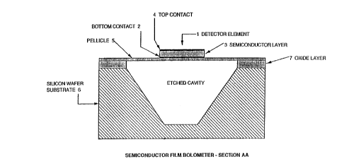
3 5 devices. Referring now to Figures 7 and 2, the detector element is
designated 1, v.
comprising bottom electrical contact 2, semiconductor layer 3, and top
electrical .
~St;BSTITUTE StfEE~
WO 91/16607
3 ~ ~ 4 PCT/AU91/0016~
contact 4. The pelllcle is designated 5, silicon wafer substrate 6, and
silicon
dioxide Insulator layer 7. Etch holes are numbered 8 and the electrical
connection joining the detector element to a nearby electronic amplifier is
shown
as 9.
The detector is prepared as follows:
The substrate is first thermally oxidised, according to established practice,
and
windows are patterned in the silicon dioxide layer so formed by conventional
i a photollthographlc techniques using a hydrofluoric acid etchant. These
windows,
which ~xtend to the surface of th~ silicon wafer, define the area where the
peilicle
Is to be formed.
A suitable material is then deposited, which will later be removed but for the
1 5 present fills the windows 1n the silicon dioxide. This material, which we
sh
all refer
to as the under-etch layer, is shown as component 10 in Figure 3. The under
etch
layer may be polycrystalline or amorphous silicon, deposited by chemical va
our
P
deposition, sputter deposition, or thermal evaporation. in an alternative
embodiment, the under-etch layer may be an amorphous dielectric material such
2 0 as a glass or silicon dioxide deposited by chemical vapour deposition. La
yers of
this latter type are widely employed in microcircuit fabrication processes.
The
main rettuirement Is that the under-etch layer can be removed by an
appropriate
etchant at a significantly faster etch rate than the window and peilicle
materials.
25 The thickness of the under-etch layers is approximately the same
as the window
depth, such that the surface of the layer is coplanar with the upper surtace
of the
oxidised wa#er. Conventional lithographic techniques are again used to a
p ttern
the under-itch layer and produce the desired geometry. in the alternative
embodiment, the under-etch layer may be deposited and planarised as a
component layer of the particular microcircuit process used for re
p paration of the
assocoated electronic circuit.
A thin dielectric film is then deposited over the entire wafer. This film,
shown as
the pellicla (5) in Figures 1, 2 and 3, must be a material having a low therm
ai
3 5 conductivity, i,n ord~r to minimise leterat heat loss from the detector
element. It Is
also desirable that the deposition parameters be selected to produce a film
with
WO 91/16607 PCT/AU91/00162
f~~ 5
.. . .... 2osi~os
low mechanical stress, so as to avoid fracture after removal
of the under-etch
layer. The preferred pellicle materials are silicon nitride or
silicon oxynitride
,~S ~/f~ y~j .
'. prepared by chemical vapour deposition. An aluminium oxide film
J,"w..;_:: deposited by
thermal evaporation, or a polyimide film prepared by established
microelectronic
processing methods, have also been found to be suitable options
for pellicie ' .
. . ... , fabrication. The thickness of the pellicls film will normally
.;;:-,y:,:,~ be in the range 50 to
250 nanometre, but polyimide films may be thicker due to the
very low thermal ,
conductivity typical of this material. ~ ,
r'
, ' ~r . 1 0 The first, or lower, contact film is then prepared as follow:
~
A thin metal film is deposited by sputter deposition or thermal
evaporation onto
the pellicle layer. This film will act as the bottom electrical
contact for the heat '. '
sensitive semiconductor layer, and may also serve as the electrical
conductor
~~ 1 5 connecting the detector element to the external electronic
circuit. The metal film is
also an essential component of the infrared absorption mechanism
of the detector '.
., design.
The desired geometrical shape of the metal film is produced by
conventional
2 0 photolithography using the lift-off technique, or alternatively
sputter or plasma ,
etching. The thickness of the film must be as small as possible
to minimise lateral
heat toss. For the same reason, the width of the film where it
forms the electrical
interconnect conductor (shown as (9) in Figure 1 ) must also
be small.
2 5 In the preferred embodiment the contact material is a thin
film of platinum or a
refractory metal such as tantalum. It should be understood that
thermal annealing
carried out during detector processing may convert the metal
to a silicide,
depending on the annealing temperature. This will be caused by
diffusion and .
reaction with the semiconductor layer which forms the heat sensitive
element of
3 0 the detector. Other metals which have been found to be suitable
options,
particularly for research purposes, include nickel or nickel-chromium
alloy.
The next process step is deposition of the semiconductor heat sensitive layer.
The preferred malarial is amorphous silicon prepared by low pressure chemical
3 5 vapour deposition (LPCVD) or by plasma-enhanced chemical vapour deposition
(PECVDj, the latter also known as RF glow discharge deposition. These
SUBSTITUTE SHEET
,.
WO 91/16607
PCT/AU91 /0016
techniques produce amorphous silicon layers from chemical dissociation of
silane gas, the resultant layer containing a varying proportion of hydrogen to
give
a material called hydrogenated amorphous silicon (a-Si:H). Sputter deposition
from a silicon cathode In the presence of hydrogen produces a layer of similar
characteristics, and this technique has been successfully employed as an
optional method of preparation.
An alternative to an a-Si:H layer is a polycrystalline silicon layer prepared
by
thermal annealing of a LPCVD silicon deposit in a manner common to fabrication
1 0 of VLSI microcircuit devices. This method may be preferred when the
detector is
prepared by high temperature processing 1n conjunction with an associated
microelectronic circuit. By comparison, a-SI:H layers are produced at lower
temperatures, and will normally be deposited affer preparation of the
microcircuit.
1 5 Depending on deposition conditions and detector geometry, the electrical
resistivity of the semiconductor layer may be of the correct order of
magnitude for
satisfactory detector performance. It may, however, be desirable to introduce
a
suitable dopant material such as boron or phosphorus by addition of a small
partial pressure of the desired gas, e.g. diborane or phosphine, during
deposition.
2 0 Alternatively, the dopant may be introduced by ion implantation. In this
manna '
r it
is possible to achieve the specified electrical reslstivity, hence resistance,
of the
detector element. The method chosen usually involves a compromise between
,the desired electrical resistivity and temperature coefficient of resistance
(TCR).
2 5 The thickness of the semiconductor layer is chosen to give optimum
infrared
absorption, as described later in this specification. The layer is patterned b
Y
conventional photolithography using a chemical etchant, or by sputter, plasma
or
reactive ion etching.
3 0 Reference should now be made to Figure 4, where three alternative contact
configurations are shown. The simple gap configuration has been previously
described; see K.C. Liddiard, Infrared Physics, Voi. 26, No. 1, p. 43, January
9 986, but may b~ considered as an alternative embodiment of the present
invention when taken in conjunction with the method of preparation described
3 5 herein. The preferred configurations, however, involve deposition of a
second or
top contact film, as illustrated in Figures 2 and 4.
. . .. . .. .... _._ _ _ . . . ........ _. ....,.. . _ .....,
_.. ....___ ......_..___~_ _~._..~___._...._ -._ , .,
y~ y S~. ~
~
~l~Jf.~C~
~~,1 ! .Y~'~f
-j
PCT/AU91/00162
.
WO 91/16607 ~~
. 1 h /, 7
~ ~
/ ,
~'
W
.. . ,
~ ( . 5
J 13
r
0
208
The top contact film will usually, but not necessarily, be of
the same composition
. as the bottom contact film, and will have a thickness chosen
to optimise infrared
' absorption. The film will again be patterned by the lift-off
technique, or by sputter
of plasma etching.
Research has shown that the electrical characteristics of the detector
contacts can
be advantageously modified by shallow doping of the semiconductor, which
assists in the achievement of low contact resistance. An ohmic contact can
also
1 0 be obtained with a thin film of pure amorphous silicon between the metal
and
semiconductor layer.
Infrared absorption may be achieved by one of two optional techniques. For the
simple gap contact configuration shown in Figure 4, the single (bottcm)
contact
1 5 layer will be deposited so as to have a nominal sheet resistance of 189
ohm per
square, giving a maximum absorption of 50%. This result is a well known
prediction of electromagnetic theory. It can be readily shown that the
thickness of ' .
the semiconductor heat sensitive layer is not critical in-so-far as infrared
absorption is concerned, but should be as small as possible to reduce planar
2 0 thermal loss.
The use of a second (top) contact, as described above, enables an enhanced
absorption to be achieved by virtue of the formation of an optical
interference
filter. The theory of this filter has been given by P.A. Silberg, in a paper
titled
2 5 "Infrared Absorption of Three-Layer Films", J. Opt. Soc. Amer., Vol. 47,
No. 7 p
575, 1957; and the application to pyroelectric infrared detectors has been
described in the article titled "Thin Film Absorber Structures for Advanced
Thermal Detectors", J. Vac. Sci. Technoi. A, Vol. 6(3), p 1688, May/June 1988.
3 0 There is, however, no known reference to the application of this technique
to
monolithic thin film bolometer infrared detectors. In this case, !he bottom
thin film
metallic contact should be a perfect reflector at infrared wavelengths, whilst
the
top contact should have a nominal sheet resistance of 377 ohm per square. The
thickness of the semiconductor heat sensitive layer must now be equal to
3 5 7U4n, where ~, is the wavelength of maximum absorption and n is the
refractive
index of the semiconductor layer. The thickness will usually be chosen to
attain
,,
Sl.II~STITUTE SHEET
WO 91/16607 ~ U g 13 ~ G 8 PCT/dU91/001~~
maximum' infrared absorption at 1 Opm wavelength.
in practice it is found that the resistance of the metallic contact films are
not critical
- an absorption of at least 90% is achieved for the 8 to l2p.m waveband when
the
resistance of the bottom contact is less than 10 ohm per square, and that of
the
top contact is 300 to 500 ohm per square.
The final process step 1s thermal isolation of the detector element, During
this
step the detector slemant must be protected by depositing a layer of a
suitable
metal or dielectric material, which acts as an etch barrier. This layer may be
aluminium, gold, silicon dioxide, silicon nitride or silicon oxyniiride. Holes
or slots
are then patterned by chemical, sputter, plasma or reactive ion etching (or a
combination of these), extending from the surface to the under-etch layer. At
this
stags It is also desirable to partially dice the substrate using a
microcircuit dicin
9
saw, to permit easy separation of Individual detector arrays after thermal
isolation.
if an under-etch layer other than silicon is employed then this layer must now
be
removed by etching through the holes or slots using the appropriate chemical
etchant. If the under-etch layer is comprised only of silicon then this step
may be
2 0 omitted.
The substrate is then loaded in a glass or teflon holder and placed in a flask
fitted
with a reflux condenser. The flask contains an anisotropic silicon etchant,
maintained at the required temperature by immersion in a temperature-
controlled
2 5 giycprot or oil bath. High purity nitrogen is circulated through the flask
an
d the
etchant is subjected to gentle agitation using magnetic stirring. The
preferred
etchant is ethylene diamine pyrocatechol (EDP). Hydrazine or potassium
hydroxide may also be used. The choice of etchant may also dictate a
ppropriate
selection of thp protective layer material.
During this process step (or steps) the under-etch layer 1s rapidly etched and
removed through the etch holes to expose the underlying manocrystaliine
silicon
substrate. The progress at this point is illustrated In Figure 3 (the
protective layer
is not shown for reasons of simplicity). The silicon substrate is then etched
to form
3 5 a pyramidal-shaped cavity beneath the detector element, conforming
precisel to
planes of crystal symmetry, y
. _ _ .. . . .. . _.. _._ __ _ . .._ _ . .. . . ....__ _. .._. ...
r as dry > " '
~<. . ~;: ,..
,.11 ~,a ~;.~~
"~.~~~'.~~', y ta!!
"~~rr. . ~~z,~,. ~'' w091/16607 Ptrl'/AU91/00162
.'~s:g:~,...h~°~~.t,,fi"3x'~~ . . . , .
a ~. .. ..t.f..:,:x :,t-r:. ~ . . ..
.. ~.!;:%.~~y4;:.11.:.'.~,t,:i . . '
_201306
Following removal of residual etchant, thence rinsing and drying, the
protective
'. ~ layer is removed and the detector elements are now seen to be supported
on
pellicles over the cavities formed in the substrate. It is noted that a
protective w
layer such as silicon nitride may be retained to add strength to the pellicle,
but this
.~T::-s~~..~:;:~.~:w:-.-;:~.;.:~ layer will contribute additional thermal
capacitance and heat loss.
Individual detector arrays may now be separated from the substrate. In this
regard; it should be understood that a number of arrays will normally be
prepared
1 0 on a single substrate by means of step-and-repeat artwork generated ort .
.
photolithographic mask sets. .
Alternative methods of thermal isolation involving anisotropic etching through
the
rear surface of the substrate have been described in references cited in this
1 5 specification. However, the present invention is concerned solely with
monolithic
single-sided wafer processing. A demonstrated option to the above procedure is
to complete the cavity etch prior to deposition of the under-etch layer, all
other
processing steps remaining the same.
20 As noted earlier, the detector array may be integrated with a
microelectronic
circuit formed on the same silicon wafer substrate: This circuit will
typically
camprise voltage blas, signal amplification, sample-and-hold, and multiplexing
components, prepared by VLSI microcircuit fabrication techniques. The choice
of '
detector materials will determine the sequence of aperations in a fully
integrated '
2 5 process schedule. Thus polysilicon and refractory silicide matallisation
can
withstand the high temperatures of VLSI processing, whilst amorphous silicon
and platinum-based matallisations must be deposited after completion of v
microcircuit preparation. ,
SUBSTITUTE SHEET
WO 91/16607
PCT/A U91 /00162
20~1~3U6 '°
Following p~ocassing, individual array chips are mounted and wire bonded in a
suitable microcircuit package. an infrared window comprised of one of the
materials germanium, silicon, zinc sulphide or zinc selenide, is sealed to the
package. Each side of the window is coated with an anti-reflection coating
optimised for infrared transmission in the 8 to 12 c.m waveband. The package
is
sealed In an atmosphere of nitrogen gas or, preferably, a gas having a low
thermal conductivity such as xenon. A novel vacuum packaging technology has
been developed, which comprises a desirable but not essential feature of the
present invention, it may be noted that sealing in a vacuum or a low thermal
conductivity gas reduces heat loss from the detector element, with a
subsequent
Increase in detector response.