Language selection

Search

Patent 2081400 Summary

Third-party information liability

Some of the information on this Web page has been provided by external sources. The Government of Canada is not responsible for the accuracy, reliability or currency of the information supplied by external sources. Users wishing to rely upon this information should consult directly with the source of the information. Content provided by external sources is not subject to official languages, privacy and accessibility requirements.

Claims and Abstract availability

Any discrepancies in the text and image of the Claims and Abstract are due to differing posting times. Text of the Claims and Abstract are posted:

  • At the time the application is open to public inspection;
  • At the time of issue of the patent (grant).
(12) Patent: (11) CA 2081400
(54) English Title: FREQUENCY SYNTHESIS USING FREQUENCY CONTROLLED CARRIER MODULATED WITH PLL FEEDBACK SIGNAL
(54) French Title: SYNTHESE DE FREQUENCE AU MOYEN D'UNE PORTEUSE A FREQUENCE COMMANDEE MODULEE PAR UN SIGNAL DE REACTION DE BOUCLE A ASSERVISSEMENT DE PHASE
Status: Deemed expired
Bibliographic Data
(51) International Patent Classification (IPC):
  • H03L 7/16 (2006.01)
  • H03J 7/02 (2006.01)
  • H03L 7/18 (2006.01)
  • H03L 7/185 (2006.01)
(72) Inventors :
  • ICHIHARA, MASAKI (Japan)
(73) Owners :
  • NEC CORPORATION (Japan)
(71) Applicants :
(74) Agent: G. RONALD BELL & ASSOCIATES
(74) Associate agent:
(45) Issued: 1998-10-27
(22) Filed Date: 1992-10-26
(41) Open to Public Inspection: 1993-04-26
Examination requested: 1992-10-26
Availability of licence: N/A
(25) Language of filing: English

Patent Cooperation Treaty (PCT): No

(30) Application Priority Data:
Application No. Country/Territory Date
3-280004 Japan 1991-10-25

Abstracts

English Abstract


In a frequency synthesizer, a phase detector receives an
externally-generated reference clock signal of a constant frequency and a feedback signal to
produce an error signal, which is output through a loop filter to a voltage-controlled
oscillator (VCO). A direct digital synthesizer (DDS) receives the reference clock
signal and externally-generated phase data to produce a DDS output signal whose
frequency is precisely controlled by the phase data. The DDS output signal is
applied as a carrier to a differential detector where it is modulated with the output
of the VCO to produce a signal corresponding to the lower sideband of the
modulated carrier. The output of the differential detector is output to the phase
detector as the feedback signal.


French Abstract

Dans un synthétiseur de fréquence, un détecteur de phase reçoit un signal d'horloge de référence externe de fréquence constante et un signal de rétroaction pour produire un signal d'erreur qui est transmis par l'intermédiaire du filtre à boucle d'un oscillateur commandé par la tension. Un synthétiseur numérique direct reçoit ce signal d'horloge de référence et des données de phase externes pour produite un signal dont la fréquence est contrôlée avec précision par ces données de phase. Ce signal est appliqué comme porteuse à un détecteur différentiel qui le module avec le signal de sortie le l'oscillateur commandé par la tension pour produire un signal correspondant à la bande latérale inférieure de la porteuse modulée. Le signal de sortie du détecteur différentiel est transmis au détecteur de phase comme signal de rétroaction.

Claims

Note: Claims are shown in the official language in which they were submitted.


THE EMBODIMENTS OF THE INVENTION IN WHICH AN EXCLUSIVE
PROPERTY OR PRIVILEGE IS CLAIMED ARE DEFINED AS FOLLOWS:

1. A frequency synthesizer comprising:
a phase detector having a reference input for receiving an
externally-generated reference signal of a constant frequency, a feedback input,and a phase detector output;
a loop filter having an input coupled to said phase detector output,
and a loop filter output;
a voltage-controlled oscillator having an input coupled to said loop
filter output, and an oscillator output for providing a synthesizer output signal;
a direct digital synthesizer (DDS) having a clock input for receiving
said reference signal, a frequency control input for receiving
externally-generated phase data, and a DDS output; and,
differential detector means having a first input coupled to said
oscillator output, a second input coupled to said DDS output for producing a
differential signal indicative of a frequency difference between signals at saidfirst and second inputs, and a differential detector output coupled to the
feedback input of the phase detector for providing the differential signal thereto.

2. A frequency synthesizer as in claim 1, wherein said direct
digital synthesizer comprises:
a phase accumulator having a phase input for receiving said phase
data, a clock input for receiving said reference signal for accumulating the
phase data at the rate of said reference signal, and an accumulator output;
a memory having a plurality of addressable storage locations each
storing a predetermined sine value, an address input coupled to said
accumulator output, and a memory output; and,
a digital-to-analog converter having a converter input coupled to
said memory output, and a converter output coupled to the second input of said
differential detector means.

11
3. A frequency synthesizer as in claim 1, wherein said
differential detector means comprises:
a mixer having a first input coupled to said DDS output, a second
input coupled to said oscillator output, and a mixer output; and,
a low-pass filter having an input coupled to the mixer output, and
an output coupled to said feedback input of the phase detector.

4. A frequency synthesizer comprising:
a phase detector having a reference input for receiving an
externally-generated reference signal of a constant frequency, a feedback input,and a phase detector output;
a loop filter having an input coupled to said phase detector output,
and a loop filter output;
a voltage-controlled oscillator having an input coupled to said loop
filter output, and an oscillator output for providing a synthesizer output signal;
and,
a differential direct digital synthesizer having:
a first phase accumulator having a clock input for
receiving said reference signal, a frequency control input for
receiving externally-generated phase data, and a first
accumulator output;
a second phase accumulator having a clock input coupled
to said oscillator output, a phase input for receiving
constant-value phase data, and a second accumulator output;
a subtractor having a first input coupled to the first
accumulator output and a second input coupled to the second
accumulator output for producing a differential signal indicative
of a frequency difference between signals at said first and
second inputs;
a memory having a plurality of addressable storage
locations each storing a predetermined sine value, address


12
inputs of the memory being coupled to the output of the
subtractor; and
a digital-to-analog converter having an input coupled to
said memory output, and an output coupled to the feedback
input of the phase detector.

5. A frequency synthesizer as in claim 1, further comprising:
a first frequency divider having an input for receiving the reference
clock signal, and an output coupled to said reference input of the phase
detector; and,
a second frequency divider having an input coupled to said
oscillator output and an output coupled to said first input of said differentialdetector means as said oscillator output.

6. A frequency synthesizer as in claim 1, wherein said loop
filter comprises a series of a low-pass filter and a band rejection filter.

7. A frequency synthesizer comprising:
reference clock means for generating a reference clock signal;
phase detector means for receiving said reference clock signal and
a feedback signal, detecting a phase difference between said reference clock
signal and said feedback signal and producing a corresponding error signal;
loop filter means for filtering noise in said error signal and
producing a filtered error signal;
variable oscillator means for generating a variable oscillator output
signal in response to said filtered error signal;
phase accumulator means for receiving a digital frequency control
signal indicative of a phase increment value and accumulating phase increment
values at a rate corresponding to said reference clock signal, and producing an
accumulator output signal corresponding to the accumulated phase increment
values;

13
memory means for storing a plurality of digital amplitude values
representing instantaneous amplitude values of an analog periodic signal and
producing a memory output signal indicative of the digital amplitude value
corresponding to each accumulated phase increment value of said accumulator
output signal;
converter means for converting the digital amplitude values of the
memory output signal to analog amplitude values, and producing a
corresponding analog periodic signal; and,
mixer means for modulating said periodic signal from said
converter means with said variable oscillator output signal, producing a mixer
output signal indicative of the modulated periodic signal, and providing the mixer
output signal as said feedback signal.

8. A frequency synthesizer as in claim 7, further comprising:
first divider means for receiving the reference clock signal, dividing
the reference clock signal frequency by a first number, and providing to said
phase detector means said reference clock signal corresponding in frequency
to said reference clock frequency divided by said first number; and,
second divider means for receiving the variable oscillator output
signal, dividing the variable oscillator output signal frequency by a second
number, and providing to said mixer means said variable oscillator output signalcorresponding in frequency to said variable oscillator output signal frequency
divided by the second number.

9. A frequency synthesizer as in claim 7, wherein said loop
filter means comprises a series of a low-pass filter and a band rejection filter.

10. A frequency synthesizer comprising:
reference clock means for generating a reference clock signal;


14
phase detector means for receiving said reference clock signal and
a feedback signal, detecting a phase difference between said reference clock
signal and said feedback signal and producing a corresponding error signal;
loop filter means for filtering noise in said error signal and
producing a filtered error signal;
variable oscillator means for generating a variable oscillator output
signal in response to said filtered error signal;
first phase accumulator means for receiving a digital frequency
control signal indicative of a first phase increment value and accumulating first
phase increment values at a rate corresponding to said reference clock signal,
and producing a first accumulator output signal corresponding to the
accumulated first phase increment values;
second phase accumulator means for receiving a digital signal of
a constant value indicative of a second phase increment value and
accumulating second phase increment values at a rate corresponding to said
variable oscillator output signal, and producing a second accumulator output
signal corresponding to the accumulated second phase increment values;
subtractor means for receiving said first and second accumulator
output signals, detecting accumulated phase difference values between the
accumulated first phase increment values and the accumulated second phase
increment values, and producing a corresponding subtractor output signal;
memory means for storing a plurality of digital amplitude values
representing instantaneous amplitude values of an analog periodic signal and
producing a memory output signal indicative of the digital amplitude value
corresponding to each accumulated phase difference value of said subtractor
output signal; and,
converter means for converting the digital amplitude values of the
memory output signal to analog amplitude values, producing a corresponding
analog periodic signal, and providing the analog periodic signal as said
feedback signal.


11. A frequency synthesizer as in claim 10, further comprising:
first divider means for receiving the reference clock signal, dividing
the reference clock signal frequency by a first number, and providing to said
phase detector means said reference clock signal corresponding in frequency
to said reference clock frequency divided by said first number; and,
second divider means for receiving the variable oscillator output
signal, dividing the variable oscillator output signal frequency by a second
number, and providing to said second phase accumulator means said variable
oscillator output signal corresponding in frequency to said variable oscillator
output signal frequency divided by the second number.

12. A frequency synthesizer as in claim 10, wherein said loop
filter means comprises a series of a low-pass filter and a band rejection filter.

13. A frequency synthesizer comprising:
a first frequency divider for receiving an externally-generated
reference clock signal of constant frequency and producing a
frequency-divided reference clock signal;
a phase detector having a reference input for receiving said
frequency-divided reference clock signal, a feedback input,
and a phase detector output;
a loop filter having an input coupled to said phase detector output,
and a loop filter output;
a voltage-controlled oscillator having an input coupled to said loop
filter output, and an oscillator output for providing a
synthesizer output signal;
a second frequency divider, connected to said oscillator output for
producing a frequency-divided synthesizer output signal;
a direct digital synthesizer (DDS) having a clock input for receiving
said externally-generated reference clock signal, a frequency


16
control input for receiving externally-generated phase data,
and a DDS output; and,
differential detector means having a first input for receiving the
frequency-divided synthesizer output signal from the first
frequency divider, a second input coupled to said DDS output
for producing a differential signal indicative of a frequency
difference between signals at said first and second inputs, and
a differential detector output coupled to the feedback input of
the phase detector for providing the differential signal thereto.

14. A frequency synthesizer as in claim 13, wherein said direct
digital synthesizer comprises:
a phase accumulator having a phase input for receiving said
phase data, a clock input for receiving said reference clock
signal for accumulating the phase data at the rate of said
reference signal, and an accumulator output;
a memory having a plurality of addressable storage locations each
storing a predetermined sine value, an address input coupled
to said accumulator output, and a memory output; and,
a digital-to-analog converter having a converter input coupled to
said memory output, and a converter output coupled to the
second input of said differential detector means.

15. A frequency synthesizer as in claim 13, wherein said
differential detector means comprises:
a mixer having a first input coupled to said DDS output, a second
input coupled to said oscillator output, and a mixer output;
and,
a low-pass filter having an input coupled to the mixer output, and
an output coupled to said feedback input of the phase
detector.


17

16. A frequency synthesizer as in claim 13, wherein said
differential detector means comprises:
a first phase accumulator having a phase input for receiving said
externally-generated phase data, a clock input for receiving
said reference clock signal for accumulating the phase data at
the rate of said reference clock signal, and a first accumulator
output;
a second phase accumulator having a phase input for receiving
constant value phase data, a clock input coupled to the output
of said second frequency divider, and a second accumulator
output;
a subtractor having a first input coupled to the first accumulator
output and a second input coupled to said second
accumulator output, and a subtractor output;
a memory having a plurality of addressable storage locations each
storing a predetermined sine value, an address input coupled
to said subtractor output and a memory output;
a digital-to-analog converter having a converter input coupled to
said memory output and a converter output; and,
a low-pass filter having an input coupled to said converter output
and an output coupled to said feedback input of the phase
detector.

17. A frequency synthesizer as in claim 13, wherein said loop
filter comprises a series of a low-pass filter and a band rejection filter.

18. A frequency synthesizer comprising:
reference clock means for generating a reference clock signal;


18

first divider means for receiving the reference clock signal and
dividing the frequency of the reference clock signal and
producing a frequency-divided reference clock signal;
phase detector means for receiving said frequency-divided
reference clock signal and a feedback signal, detecting a
phase differential between said frequency-divided reference
clock signal and said feedback signal and producing a
corresponding error signal;
loop filter means for filtering noise in said error signal and
producing a filtered error signal;
variable oscillator means for generating a variable oscillator output
signal in response to said filtered error signal;
second divider means for receiving the variable oscillator output
signal, dividing the frequency of the variable oscillator output
signal and producing a frequency-divided variable oscillator
output signal;
phase accumulator means for receiving a digital frequency control
signal indicative of a phase increment value and accumulating
phase increment values at a rate corresponding to said
reference clock signal from said reference clock means, and
producing an accumulator output signal corresponding to the
accumulated phase increment values;
memory means for storing a plurality of digital amplitude values
representing instantaneous amplitude values of an analog
periodic signal and producing a memory output signal
indicative of the digital amplitude value corresponding to each
accumulated phase increment value of said accumulator
output signal;
converter means for converting the digital amplitude values of the
memory output signal to analog amplitude values, and
producing a corresponding analog periodic signal; and,


19

mixer means for modulating said periodic signal from said
converter means with said frequency-divided variable oscillator
output signal, producing a mixer output signal indicative of the
modulated periodic signal, and providing the mixer output
signal to said phase detector means as said feedback signal.

19. A frequency synthesizer as in claim 18, wherein said loop
filter means comprises a series of a low-pass filter and a band rejection filter.

20. A frequency synthesizer comprising:
reference clock means for generating a reference clock signal;
phase detector means for receiving said reference clock signal
and a feedback signal, detecting a phase difference between
said reference clock signal and said feedback signal and
producing a corresponding error signal;
loop filter means for filtering noise in said error signal and
producing a filtered error signal;
variable oscillator means for generating a variable oscillator output
signal in response to said filtered error signal;
first phase accumulator means for receiving a digital frequency
control signal indicative of a first phase increment value and
accumulating first phase increment values at a rate
corresponding to said reference clock signal, and producing a
first accumulator output signal corresponding to the
accumulated first phase increment values;
second phase accumulator means for receiving a digital signal of
a constant value indicative of a second phase increment value
and accumulating second phase increment values at a rate
corresponding to said variable oscillator output signal, and
producing a second accumulator output signal corresponding
to the accumulated second phase increment values;


subtractor means for receiving said first and second accumulator
output signals, detecting accumulated phase difference values
between the accumulated first phase increment values and the
accumulated second phase increment values, and producing
a corresponding subtractor output signal;
memory means for storing a plurality of digital amplitude values
representing instantaneous amplitude values of an analog
periodic signal and producing a memory output signal
indicative of the digital amplitude value corresponding to each
accumulated phase difference value of said subtractor output
signal; and,
converter means for converting the digital amplitude values of the
memory output signal to analog amplitude values, producing
a corresponding analog periodic signal, and providing the
analog periodic signal as said feedback signal.

21. A frequency synthesizer as in claim 20, further comprising:
first divider means for receiving the reference clock signal, dividing
the reference clock signal frequency into a divided reference
clock signal frequency, and providing to said phase detector
means said reference clock signal corresponding in frequency
to said divided reference clock signal frequency;
second divider means for receiving the variable oscillator output
signal, dividing the variable oscillator output signal frequency
into a divided variable oscillator output signal frequency, and
providing to said second phase accumulator means said
variable oscillator output signal corresponding in frequency to
said divided variable oscillator output signal frequency.

22. A frequency synthesizer as in claim 20, wherein said loop
filter means comprises a series of a low-pass filter and a band rejection filter.


Description

Note: Descriptions are shown in the official language in which they were submitted.


~0~ 1 400


FREQUENCY SYNTHESIS USING FREQUENCY CONTROLLED
CARRIER MODULATED WITH PLL FEEDBACK SIGNAL

The present invention relates generally to phase-lock-loop
frequency synthesizers, and more specifically to a direct-digital-synthesizer-
driven phase-lock-loop frequency synthesizer which is particularly suitable for
use in applications, such as digital cellular telephony, where communications
5 channels are switched from one channel to another at significantly high speeds.
As shown in Figure 1a, a typical conventional phase-lock-loop
frequency synthesizer synthesizes a frequency by using a control voltage to
drive a voltage-controlled oscillator (VCO) 5, which generates a signal of
frequency fO near the desired frequency. A frequency divider 6 is used to divide10 the VCO-signal output frequency by an integer value N to produce a signal of
frequency fs The frequency-fs signal is input along with a signal of reference
frequency fr to a phase detector 3. The phase detector compares the
frequencies of the two input signals and outputs a voltage proportional to the
difference in frequency of the two input signals. The output of the phase
15 detector 3 is coupled through a loop filter 4, where it is input to the VCO 5 as
the control voltage. The reference frequency (fr) signal is derived by a divide-by-M frequency divider 2 which divides a signal of high-accuracy frequency fx
from a master oscillator 1 by a constant integer value M. The integer N of
frequency divider 6 is variable by an incremental-frequency-control voltage so
20 that if the VCO 5 were generating exactly the desired frequency, the resultant
frequency-fs signal would be exactly the same frequency as reference frequency
fr and the following relation would hold:

fo = (N)(fx / M) (1 )
As the frequency-control voltage is varied, the output frequency fO varies
25 accordingly from one frequency, or channel, to another, and the minimum
channel separation, or frequency step size or resolution, /\fO, is given by:
~fo = fx / M (2)

{~8~ 400
-


To insure loop stability the loop filter needs to have a cutoff frequency much
lower than the reference frequency. However, the lock-in time of the frequency
synthesizer is inversely proportional to the cutoff frequency. Since the reference
frequency is predetermined, the lock-in time cannot be reduced and hence is a
5 detrimental factor to achieving high-speed channel switching.
This slow lock-in operation is overcome by techniques shown and
described in United States Patent 4,965,533. To provide mathematical analysis
of this patent, two embodiments of the prior art PLL frequency synthesizer are
shown respectively in Figures 1 b and 1 c of this specification. One of the prior-
10 art embodiments, shown in Figure 1b, incorporates a direct digital synthesizer(DDS) 7 that is clocked by the master oscillator to serve as the source of the
reference frequency for the phase-lock loop. The DDS typically comprises a
phase accumulator which receives a digital fine-frequency control signal l\X to
determine the phase increment for accumulation at the master clock rate. The
15 accumulated phase value is output to a sine lookup table, which stores sine
values and provides an output signal, indicative of the digital representation of
a periodic waveform, as an input to a digital-to-analog converter. The output ofthe D/A converter is filtered by a low-pass filter 8 and input to the frequency
divider 2, whose output is used as a variable reference-frequency input to the
20 phase detector. Thus, frequency divider 6 operates as a constant-value divider.
When the accumulated phase reaches a certain threshold, the phase
accumulator automatically resets itself to repeat the accumulation process.
Thus, the phase accumulator can be said to operate with a modulo value. If
this modulo value is represented as L, the reference frequency fr is given by:
fr = (fx)(~X) / L (3)

and the synthesizer output frequency fO is expressed by:

fO = (N)(fr) = (N)(fx)(~\X) / L (4)
Since the frequency control is provided by DDS 7 in response to increment ~X,
the minimum frequency step size l~fO is equal to a variation in the output

? ~ ~ ~ 9
rA~
j,??r"-

~ ~ 3 1 4 0 0


frequency fO that occurs in response to an increment of I~X = 1. Therefore, the
following relation holds:

~fO = (N)(fx / L) (5)
From Equations (3) and (5), the relation fr = (~fo)(~X / N) is
5 obtained. This implies that by setting the increment ~X at a value greater than
the integer N, the reference frequency fr can be set higher than the reference
frequency of the Figure 1 a frequency synthesizer for a given minimum
frequency resolution. For example, using a minimum frequency step size of 25
kHz, a master clock frequency fx = 12.8 MHz and an integer N = 1024, Equation
(5) gives a modulo value L = 219. If the output frequency fO is chosen at 1
GHz, Equation (4) gives an increment ~\X = 40000, a value much greater than
the integer N = 1024. Thus, a reference frequency of 976.5625 kHz, much
higher than l~fo = 25 kHz, is obtained. While high-speed convergence of the
phase-lock loop can be achieved, variation of the reference frequency causes
15 a control voltage variation at the input of the VCO, a variation known as
"reference leak", which would result in the transmission of spurious frequencies.
A band rejection filter must be provided as part of the loop filter 4 to eliminate
the undesired spurious transmission. However, it is difficult to eliminate the
undesirable components uniformly across all channels of the frequency
20 synthesizer.
According to the other prior art technique shown in Figure 1 c, DDS
7 and low-pass filter 8 are provided in the phase-lock loop, following the output
of divider 6, so that the divided frequency signal fs is caused to vary in
response to phase increment l~X, while reference frequency fr remains constant,
25 thus giving the following relations:

fs = (fo)(l\X) / (N)(L) (6)
fx / M = (fo)(l\X) / (N)(L)
Thus, fo = (fX)(N)(L) / (M)(l\x) (8)


~,

400
.

While this technique eliminates the reference leak problem, the fact that the
output frequency fO varies inversely proportional to the increment l\X, as givenby Equation (8), makes it impossible to set all channels of the synthesizer at
precisely-equal frequency intervals.
It is therefore an object of the present invention to provide a
phase-lock-loop frequency synthesizer that allows high-speed setting of a
selected frequency from a plurality of precisely-equally-spaced-apart frequencies
without causing reference leak.
According to the present invention, there is provided a frequency
synthesizer which comprises: a phase detector having a reference input for
receiving an externally-generated reference signal of a constant frequency, a
feedback input, and a phase detector output; a loop filter having an input
coupled to the phase detector output, and a loop filter output; and, a voltage-
controlled oscillator having an input coupled to the loop filter output, and an
oscillator output for providing a synthesizer output signal. It also comprises adirect digital synthesizer (DDS) having a clock input for receiving the reference
signal, a frequency control input for receiving externally-generated phase data,and a DDS output. It further comprises a differential detector means having a
first input coupled to the oscillator output, a second input coupled to the DDS
output for producing a differential signal indicative of a frequency difference
between signals at the first and second inputs, and a differential detector output
coupled to the feedback input of the phase detector for providing thereto the
differential signal.
The direct digital synthesizer comprises: a phase accumulator
having a phase input for receiving the phase data, a clock input for receiving the
reference signal for accumulating the phase data at the rate of the reference
signal, and an accumulator output; a memory having a plurality of addressable
storage locations each storing a predetermined sine value, an address input
coupled to the accumulator output, and a memory output; and, a digital-to-
analog converter having a converter input coupled to the memory output, and
a converter output coupled to the second input of the differential detector

' ' ! ' ~ ' r~ ~

~u~ ~ 400


means. The differential detector means may comprise a mixer having a first
input coupled to the DDS output, a second input coupled to the oscillator output,
and a mixer output; and, a low-pass filter having an input coupled to the mixer
output, and an output coupled to the feedback input of the phase detector.
According to a second embodiment of the present invention, the
direct digital synthesizer (DDS) and the differential detector means are replaced
by a differential direct digital synthesizer which comprises first and second
phase accumulators, a subtractor, a memory and a digital-to-analog converter.
The first phase accumulator has a clock input for receiving the reference signal,
a frequency control input for receiving externally-generated phase data, and a
first accumulator output. The second phase accumulator has a clock input
coupled to the oscillator output, a phase input for receiving constant-value
phase data, and a second accumulator output. The subtractor has a first input
coupled to the first accumulator output and a second input coupled to the
second accumulator output for producing a differential signal indicative of a
frequency difference between signals at the first and second inputs. The
memory has a plurality of addressable storage locations each storing a
predetermined sine value, address inputs of the memory being coupled to the
output of the subtractor. The digital-to-analog converter has an input coupled
to the memory output, and an output coupled to the feedback input of the phase
detector.
Preferably, the frequency synthesizer includes a first frequency
divider having an input for receiving the reference clock signal, and an output
coupled to the reference input of the phase detector; and, a second frequency
divider having an input coupled to the oscillator output and an output coupled
to the first input of the differential detector means as the oscillator output. The
loop filter may comprise a series of a low-pass filter and a band rejection filter.
The present invention will be described in further detail with
reference to the accompanying drawings, in which:
Figure 1a is a block diagram of a conventional phase-lock-loop
frequency synthesizer;

. .~.
.. , -.~
~rA~

. CA 02081400 1998-0~-12


Figures 1b and 1c are block diagrams of the phase-lock-loop
frequency synthesizers of the aforesaid U.S. Patent 4,965,533;
Figure 2 is a block diagram of a first embodiment of the subject
invention; and
Figure 3 is a block diagram of a second embodiment of the subject
invention.
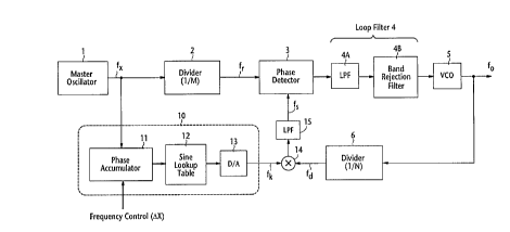
Referring now to Figure 2, there is shown a phase-lock-loop
frequency synthesizer according to a first embodiment of the present invention.
The PLL frequency synthesizer of the present invention comprises a direct
digital synthesizer 10 which is clocked by the master oscillator 1. DDS 10
includes a phase accumulator 11 which operates with modulo L and receives
a digital fine-frequency control signal ~\X to determine the phase increment foraccumulation at the master clock rate. The accumulated phase value is output
to a sine lookup table 12, which stores sine values and uses the accumulated
phase value as an address signal to provide an output signal, indicative of the
digital representation of a sinusoidal waveform at frequency fk, as an input to a
digital-to-analog converter 13. Sine lookup table 12 is typically implemented
with a read-only memory. The output of the D/A converter 13 is input to an
analog mixer 14 as a local carrier and mixed with the output signal of frequencyfd from frequency divider 6 to produce a signal that is indicative of the amplitude
modulation of the divided frequency signal fd. The output of mixer 14 is filtered
by a low-pass filter 15 to remove undesired higher frequencies and input to
phase detector 3 as a signal of frequency f5.
The embodiment of Figure 2 can be analyzed as follows:

fk (fx)(~x) / L
fd = fO / N (10)
fs = fd ~ fk = (fO / N) - (fX)(~X) / L (11)
Since fr = fx / M, and fr = f5 when the frequency synthesizer converges, the
following Equation holds:

~J ~ 1 4 0 0


fx / M = (fO / N) - (fX)(l~X) / L (12)

Thus, the output frequency fO and the minimum frequency step size QfO of the
frequency synthesizer are given as:
fO = (N)(fx){L + (I\X)(M)} / (L)(M) (13)
~fO = (N)(fx) / L (14)

Equation (13) indicates that all channels of the synthesizer can be
set at precisely-equal frequency intervals. In addition, since Equation (14) is
identical to Equation (5), the minimum frequency step size of the present
embodiment is as small as that of the prior art of Figure 1b. A further
10 advantage is that, by virtue of the constant reference frequency, reference leak
can be easily removed by a simple band rejection filter 4B which, together with
a low-pass filter 4A, forms the loop filter 4. Moreover, the reference frequencycan be chosen as a desired high value regardless of the step size ~fO, and the
frequency synthesizer can then be converged at a high speed.
With a step size of 25 kHz, a master clock frequency fx = 12.8
MHz and an integer N = 512, Equation (14) gives a modulo value of L = 218.
If the integer M is set equal to 8 and the desired output frequency fO is 1 GHz,Equation (13) provides I~X = 7232. A reference frequency fr of as high as 1.6
MHz can therefore be obtained, which is suffficiently high to achieve high-speedconvergence.
It is preferable to implement phase-lock-loop frequency
synthesizers using LSI technology. A second embodiment of the present
invention, shown in Figure 3, is suitable for the LSI implementation. This
embodiment differs from the first embodiment by the use of a differential DDS
20 instead of the DDS 10 and mixer 14 of the previous embodiment. It is seen
that differential DDS 20 is comprised of a first phase accumulator 21 clocked bythe master oscillator 1 at frequency fx and a second phase accumulator 22
clocked by the frequency divider 6 at frequency fd. Each phase accumulator
has a modulo value of L as in the accumulator of the previous embodiment.

.,, . ,; . .
I~.''A'' r
~ a ~

~0~ t 400


Phase accumulators 21 and 22 feed their output signals to a digital subtractor
23 which detects the difference between the two inputs, and outputs a signal
indicative of the difference to a sine lookup table 24 as an address signal. A
periodic signal is generated by sine lookup table 24 and is output to D/A
5 converter 25. The output of D/A converter 25 is coupled to the low-pass filter15.
Phase accumulator 21 receives a digital fine-frequency control
signal Xa to determine the phase increment for accumulation at the master
clock rate, while phase accumulator 22 receives a fixed digital value ~\Xb to
10 determine the phase increment for accumulation at a clock rate which is 1 / N of the VCO output frequency.
By setting l~Xa equal to a non-zero value and l~Xb equal to zero,
the differential DDS 20 operates as if it were a normal, single-accumulator DDS
clocked at the master clock rate, and in this case, the output frequency fs1 ~f
15 differential DDS 20 is given by:

fs1 (fx)(~xa) / L (15)
Conversely, if QXa is set equal to zero and l\Xb to a non-zero
value, the differential DDS 20 operates as if it were a normal, single-
accumulator DDS clocked at the rate of the output of frequency divider 6, and
20 in this case, the output frequency fs2 of differential DDS 20 is given by:
fs2 (fd)( Xb) / L = (fo)(~\Xb) / (L)(N~) (16)

where N' is the integer of divider 6 when the differential DDS 20 is clocked
exclusively by the output of divider 6.
Therefore, if both of the phase increments ~Xa and ~Xb are of
25 non-zero value, the output frequency fs of differential DDS 20 is represented as:

fs fs2 ~ fs1 = (fo)(~Xb) / (L)(N ) - (fx)(~Xa) / L (17)
By setting N' = (N)(l~Xb) / L, and ~Xa = I~X, Equation (17) can be rewritten as:fs = (fo)(N) - (fx)(~X) / L (18)

A~~
,~ ~,

~u&l 400
.


Since Equation (18) is identical to Equation (11), the frequency synthesizer of
the second embodiment operates exactly in the same manner as that of the first
embodiment.


. .~
J
A .:
. ~. ~~i
" ~

Representative Drawing
A single figure which represents the drawing illustrating the invention.
Administrative Status

For a clearer understanding of the status of the application/patent presented on this page, the site Disclaimer , as well as the definitions for Patent , Administrative Status , Maintenance Fee  and Payment History  should be consulted.

Administrative Status

Title Date
Forecasted Issue Date 1998-10-27
(22) Filed 1992-10-26
Examination Requested 1992-10-26
(41) Open to Public Inspection 1993-04-26
(45) Issued 1998-10-27
Deemed Expired 2002-10-28

Abandonment History

There is no abandonment history.

Payment History

Fee Type Anniversary Year Due Date Amount Paid Paid Date
Application Fee $0.00 1992-10-26
Registration of a document - section 124 $0.00 1993-07-23
Maintenance Fee - Application - New Act 2 1994-10-26 $100.00 1994-10-25
Maintenance Fee - Application - New Act 3 1995-10-26 $100.00 1995-10-25
Maintenance Fee - Application - New Act 4 1996-10-28 $100.00 1996-10-18
Maintenance Fee - Application - New Act 5 1997-10-27 $150.00 1997-10-17
Final Fee $300.00 1998-05-14
Maintenance Fee - Application - New Act 6 1998-10-26 $150.00 1998-10-16
Maintenance Fee - Patent - New Act 7 1999-10-26 $150.00 1999-10-14
Maintenance Fee - Patent - New Act 8 2000-10-26 $150.00 2000-10-02
Owners on Record

Note: Records showing the ownership history in alphabetical order.

Current Owners on Record
NEC CORPORATION
Past Owners on Record
ICHIHARA, MASAKI
Past Owners that do not appear in the "Owners on Record" listing will appear in other documentation within the application.
Documents

To view selected files, please enter reCAPTCHA code :


To view images, click a link in the Document Description column. To download the documents, select one or more checkboxes in the first column and then click the "Download Selected in PDF format (Zip Archive)" or the "Download Selected as Single PDF" button.

List of published and non-published patent-specific documents on the CPD .

If you have any difficulty accessing content, you can call the Client Service Centre at 1-866-997-1936 or send them an e-mail at CIPO Client Service Centre.


Document
Description 
Date
(yyyy-mm-dd) 
Number of pages   Size of Image (KB) 
Abstract 1994-01-29 1 29
Cover Page 1994-01-29 1 20
Description 1997-10-09 9 379
Claims 1997-10-09 11 450
Abstract 1997-10-09 1 20
Representative Drawing 1998-10-16 1 6
Description 1994-01-29 9 451
Drawings 1994-01-29 3 86
Claims 1994-01-29 6 258
Drawings 1997-10-09 3 49
Description 1998-05-12 9 378
Cover Page 1998-10-16 1 53
Fees 1999-10-14 1 44
Correspondence 1998-05-12 2 63
Correspondence 1998-05-14 1 36
Correspondence 1997-11-17 1 90
Fees 1998-10-16 1 46
Fees 1997-10-17 1 45
Fees 2000-10-02 1 44
Prosecution Correspondence 1992-10-26 1 36
Prosecution Correspondence 1997-01-10 17 666
Office Letter 1993-05-21 1 52
Examiner Requisition 1996-10-21 2 81
Fees 1996-10-18 1 58
Fees 1995-10-25 1 38
Fees 1994-10-25 1 36