Note: Descriptions are shown in the official language in which they were submitted.
~~~~~~z
1
TRANSPONDER SYSTEM
The present invention relates in general to
communication systems, and more particularly to an
electronic identification system comprising one or more
portable transponders for transmitting an information
signal in response to entering an electromagnetic
excitation field.
Electronic identification systems are well known in
the art for effecting automatic identification of objects,
animals and people, and are used in situations where
elementary line of sight systems such as bar codes cannot
be used. Such prior art identification systems typically
comprise a plurality of electronic transponders (commonly
~5 ref erred to as electronic tags or simply tags) which are
attached to the particular objects to be identified, and at
least one interrogator (that is a controlled transmitter
and receiver, sometimes referred to as a reader) for
exciting the transponders into transmitting response
signals which are then detected by the interrogator,
decoded and converted into information for display to a
human operator, or transmitted as data to a computer.
One such identification system is described in United
Kingdom patent application GB 2,112,607 (Senelco Limited),
published on July 20, 1983, which discloses a system
comprising a transponder having a receiver for receiving a
transmitted signal S1, a generator for generating a further
carrier signal S2, logic means for modulating the signal S2
according to a coded mathematical relationship with the
received signal S1, and a transmitter for transmitting the
signal S2. Specifically, the carrier frequency of the
signal S2 is disclosed as being a multiple or a fraction of
the frequency S1.
United Kingdom patent application GB 2,157,132
(Senelco Limited), published on October 16, 1985, also
discloses an identification system of the form discussed.
above in connection with the '607 specification, but in
2
addition incorporates circuitry for receiving a reply
signal (e. g. information signal) from the transponder,
checking the reply signal for possible contention between
reply signals from different transponders which arrive at
the same time, and initiating retransmission of the reply
signals in the event such a contention situation is
detected. Specifically, the tag receives a signal from the
interrogator which it compares with stored information in
order to determine whether the message transmitted by the
tag has been received by the interrogator for confirming
that the tag has been identified by the interrogator and
can therefore fall silent. Contention in this system is
resolved by sophisticated duplex communications between
reader and tag in order to achieve simultaneous
identification of numerous tags.
As with the '607 specification, the circuitry in the
'132 disclosure incorporates means for deriving a received
carrier signal at the transponder, and using the derived
carrier signal to provide a transmission signal which is
related to and therefore dependent on the sustained
presence of the received signal from the interrogator.
Additional prior art systems are well known for
teaching transmission of the transponder information
signals which are dependent on the received interrogation
signal, as follows:
European patent application 0,310,127 (Texas
Instruments), published on February 1, 1989, teaches a
transponder arrangement which transmits an information
signal at a predetermined carrier frequency related to the
frequency of a received RF interrogation pulse.
United Kingdom patent application GB 2,202,981
(Satellite Video Systems Ltd.), published on October 5,
1988, discloses a system incorporating a transponder
designed to modify a received interrogation signal in a
variable manner and then retransmit the modified signal for
reception by the interrogation unit.
United Kingdom patent application GB 2,163,324
'~' 3
(Electromatic), published on 19 February 1986, discloses a
system in which energy is extracted from a detected
interrogation signal, compared to a reference level and
then supplied to the remainder of the transponder circuit
for enabling generation and transmission of the information
signal.
European patent application 0,253,368 (Amtech
Corporation), published on 20 January, 1988, discloses an
identification system comprising a reader and a
transponder, the transponder being adapted to receive an
interrogation signal and in response generate a modulated
response.
A fundamental disadvantage of such prior art systems
in which the information signal transmitted by the
transponder is related to (i.e. dependent on) the received
interrogation signal, is that in situations in which there
is fast relative movement between the transponder and the
interrogator there may be insufficient time for the
transponder to extract the carrier signal and thereby have
the means to generate and transmit the required information
signal. specifically, tags such as those described in GB
2,112,607 and GB 2,157,132 which require the sustained
presence of the excitation field in order to provide a
response signal, will cease transmitting immediately once
the excitation signal falls below a certain level. Since
the interrogator in these systems expects to sample data
from the tags in bit-contiguous format, sampled with
respect to the interrogator's transmit clock reference
signal, data sampled by the interrogator will be corrupted
and the partial message must be discarded. This is a real
practical problem with previous systems where the level of
signal detected by a tag is highly dependent upon the
relative orientation of tag and excitation antennae,
WO 91/17515 PCT/CA91/00147
4 A~~ ~~
such that as a tag passes an antenna it may at various
times during its passage go through nulls when it will
cease transmission. The problem is especially acute
in systems such as that disclosed in GB 2,112,607 "
where the tag transmits its stored data at a very low
rate.
In addition, such prior art interdependence
between the frequency of the excitation signal and the
frequency of the transmitted information signal
imposes practical limitations on the frequency range
of signals which can be used for interrogation and
transmission of the information. The rigid
mathematical (harmonic) relationship between the
excitation and response signals in systems such as
that disclosed in GB 2,112, 607 further complicates the
design of the receiver in the interrogator. It is
almost inevitable that harmonic components of the
excitation carrier signals will be present and these
must be eliminated from the signal reception channel
in order to yield an acceptably high signal to noise
ratio.
A further disadvantage of such prior art systems
is that the transponder is typically tuned to a
specific frequency depending on the particular
application. For example, communications using low
frequency electromagnetic signals are ideal in
situations where the transponder is enveloped in
material which causes significant attenuation of radio
signals, such attenuation being much less pronounced
at low frequencies than high frequencies. However,
such transponders which are receptive to low frequency
excitation signals would be inappropriate. for
applications in which a degree of directionality is
required. An example of such an application would be
the use of a transponder which is receptive to
microwave signals wherein a portable reader and
antenna can be aimed at a target object amongst a
WO 91 / 17515 ~ ~ ~ ~ PCT/CA91 /00147
group of objects each with an attached transponder in
order to identify the particular object. A
transponder which is receptive to microwave signals
offers the opportunity to design such a directional
5 system and identify transponders at a greater range
than when using low frequency~excitation signals.
In certain applications, where objects with
attached transponders move around a large site or from
one site to another, it is possible that at certain
times optimum performance would be achieved using a
microwave excitation signal yet at other times peak
performance would be achieved using a low frequency
excitation signal. A practical example of this
scenario is the identification of air cargo
containers. At times the containers may be resting on
a concrete apron at an airport such that line-of-sight
identification is possible using a microwave
excitation signal, while at other times the containers
are in the holds of aircraft or maybe in a warehouse
or loading/unloading area which may be constructed
partly of metal. Since microwave signals behave in a
manner similar to light, problems resulting from
reflection of the microwave signals can give rise to
uncertainty about the path of the excitation signal
and potentially cause excitation of more than one
transponder inadvertently.
A second disadvantage associated with the single
excitation frequency of the prior art transponders is
that, for general applications, government regulatory
authorities do not typically grant exclusive use of
predetermined operating frequencies to the user of a
transponder identification system. This means-that
the users must operate in certain approved frequency
bands which are often shared with, for example, low
power telemetry systems., As such, the transponder
identification system is subject to interference from
other signals which may originate from intentional
r
A~~~~
2 7. 04. 92
6
radiators also operating in a particular frequency band or
from high powered equipment generating spurious signals
which fall within the frequency band used by the
transponder. Conversely, a transponder identification
system operating in such a band may cause interference to
other systems sharing the same band width. Thus, it may
not be possible to install a transponder identification
system at a particular location because of interference
from external signals in the same frequency band, resulting
in severe degradation in performance of the identification
system, or the risk of causing interference to the other
systems.
A further prior art electronic identification system
is disclosed in FR A 2 604 808 (Bazin) which teaches the
use of a radio electric receiver which waits to receive a
coded signal which is adequate to start up a timing
processor. When the latter is activated, it activates a
radio electric emitter, then activates a memory-reading
processor, waits for the end of the information transfer,
stops the radio electric emitter and waits for a fraction
of a second before returning to stand-by. However, as with
the prior discussed references, there is no teaching in the
Bazin reference of generating an information signal at a
frequency which is neither derived from nor related to the
frequency of the electro-magnetic excitation field.
It is an object of an aspect of the present invention
to provide an electronic identification system comprising:
a) means for generating an electromagnetic
excitation field at a first variable frequency,
b) portable transponder means for storing variable
identification data, and for transmitting at a second
variable frequency an information signal containing said
. 35 data upon entering said field, said transmitting of said
signal being independent of said transponder means
r
6a
remaining in said field, said second variable frequency
being neither derived from nor related to said first
variable frequency of the electromagnetic excitation field,
c) means for receiving said information signal and
in response generating an output signal representing said
variable identification data contained in said information
signal.
It is also an object of an aspect of the present
invention to provide a transponder which can produce a
response signal whose frequency can be set according to the
conditions encountered at a particular site, thereby
maximizing the range of applications and sites to which the
system may be applied without modification of the
transponder's circuits. This can be seen to have further
advantage, where in the absence of internationally
acceptable operating frequencies for these transponder
systems, it would be possible to have a transponder
attached to an intermodal container, for example,
identified at the point of loading onto a ship in one
country, with the transponder set to produce a response
signal at frequency fl, say, then on arrival in another
country instructed to change the frequency of its response
' 25 channel so that it could be identified by receiving signals
at frequency f2, say, where neither frequency fl, or f2, were
acceptable in both origin and destination countries.
According to the present invention, an electronic
identification system is provided having a portable
transponder for generating and transmitting an
identification or information signal independently of
oy ~
,~, . . ~: :.
WO 91/17515 ~ ~ PCT/CA91/00147
7
continued presence of the interrogation signal. Thus,
the system of the present invention may be operated
with interrogation and information signals from
virtually any frequency over the entire
electromagnetic spectrum (e.g. ranging from DC at the
low frequency end of the spectrum to light frequency
at the high frequency end). In addition, the system
of the present invention may be utilized in
applications where there is fast relative movement
between the transponder and the interrogator.
According to a preferred embodiment of the
invention, a transponder is provided which is
selectively responsive to various excitation
frequencies, thereby facilitating performance
optimization according to predetermined applications
and operating specifications.
According to an additional aspect of the
invention, digital signal inputs are provided for the
transponder, in order to sample external inputs and
report back the results along with the identification
information, thereby permitting remote monitoring of
the state of digital signals representing physical
variables such as temperature or pressure.
According to a further aspect of the invention,
the information signal may be encrypted prior to
transmission using a pseudo-random varying key
generated automatically by the tag.
In addition, the transponders of the present
invention are reprogrammable during use, by means of
modulated radio signals generated by the interrogator.
Furthermore, the tag according to the present
invention formats and transmits data at standard
rates, the precise nature of which is a programmable
feature of the tag, which means that a reader may in
its simplest form comprise the excitation signal
generator (transmitter) and signal receiver alone
without there being the need for a data processing
WO 91/17515 PCT/CA91/00147 "~",
element (e. g. a microprocessor). Post demodulation,
the format of data received from a tag is such that it
can be presented directly to a computer via a serial
interface, operating in either a synchronous or
asynchronous reception mode.
This is a radical departure from previous systems
in which the rate and format of the data transmitted
by a tag are such that it must be processed (either in
format and/or rate) prior to being offered to a
computer via a standard serial interface.
A preferred embodiment of the invention will be
described in greater detail below with reference to
the following drawings, in which:
Figure 1 is a block diagram of the identification
system according to the present invention;
Figure 2 is a block diagram of the transponder or
tag in accordance with a first embodiment;
Figure 3 is a partial schematic/block diagram of
the transponder illustrated in Figure 2;
Figures 4a-4e illustrate the character and
message composition of the information signal
transmitted by a tag, in accordance with the present
invention;
Figure 5 is a block diagram of the transponder on
tag in accordance with the preferred embodiment; and
Figure 6 is a partial schematic block diagram of
the transponder illustrated in Figure 5.
Turning to Figure 1, a block diagram of the
identification system of the present invention is
shown in its most general aspect. The system
comprises an interrogator/reader (herein referred to
as reader 1) and a plurality of transponders (herein
referred to as tags 3) which are attached to objects
to be identified (e. g. animals, people, vehicles,
etc.). The reader 1 generates an excitation field by
means of a radio frequency (RF) transmitter 5
connected to a transmit antenna 7. Respective ones of
WO 91/17515 ~ '~ ~ ~ ~ PCT/CA91/00147
9
the tags 3 are adapted to transmit the response or
information signals for, among other things,
identifying the associated object.
The reader 1 receives the information signals by
means of a receive antenna 9 connected to an RF
receiver 11. The received information signals are
decoded and converted into a suitable output signal by
means of microcontroller 13 and serial input/output
circuit 15 for display to a human operator, or for use
l0 by a computer or other monitoring equipment 17.
As will be discussed in greater detail below,
each of the tags 3 is in the form of a miniature radio
frequency receiver and transmitter, which can store
and transmit the coded information signal upon
detecting the excitation signal, for conveying the
identity and other characteristics of the associated
object to the reader 1. The circuitry of the tags 3
are sealed in respective small, light weight plastic
cases. Information stored in the tags 3 may be
altered by means of variable control signals generated
by transmitter 5 and antenna 7 under control of
microcontroller 13, and may be modified by a user
according to specific individual requirements.
Furthermore, the tags 3 may, if required, be write-
protected so that the data may not be changed.
The microcontroller 13 of reader 1 detects,
analyses and formats the information signal received
from the tags 3, and presents error free information
in a variety of formats, as required by each
individual application.
Serial input/output port 15 allows for direct
connection of the reader 1 to a computer or other
monitoring equipment 17. In addition, reader 1 is
provided with output ports which are electrically and
functionally compatible with industry standard
identification and data capture systems such as
magnetic card reader heads and bar code wands, in
WO 91/17515 PCT/CA91/00147
addition to the duplex serial communications port 15
for connection to a computer. Thus, these special,
dedicated output ports allow for easy integration of
the reader 1 into existing identification and data
5 capture systems without modification to the system
software .
For the purposes of describing a practical
system, the RF transmitter 5 shall be a low frequency
(LF) transmitter. Antenna 7 is in the form of a
10 simple tuned or untuned wire loop which generates an
electromagnetic field for exciting the tags 3. As
discussed above, the transmit antenna ? is driven by
transmitter 5 and is connected to the reader 1
preferably by means of a screw terminal connector for
convenience and ease of installation. The size of the
loop is determined by each application, and may be as
small as approximately 50mm diameter where only short
range operation is required, or may be wound round a
door frame or other similar sized aperture in
applications requiring the identification of
personnel.
Microcontroller 13 is configurable for operation
in many user defined modes, as required for each
application. The configuration information is stored
in an electrically erasable, non-volatile memory
(EZPROM) under control of microcontroller 13. For
example, the reader 1 may be configured to transmit
information every time it reads data from a tag 3, or
alternatively to transmit data from a particular tag
3 once only following an initial detection.
In operation, the reader 1 essentially emulates
a card reader or bar code wand according to well known
techniques, and generates an output signal in the form
of serial logic presented via integrated output ports.
The reader 1 may be powered by a regulated or an
unregulated DC or AC supply, in a well known manner.
The power supply 19 regulates the input power signal
WO 91/17515 PCT/CA91/00147
11
and derives a local +5 V DC signal for internal logic
circuitry (e.g. microcontrolher 13) as well as a
+12 V DC signal for the analogue circuits (e. g.
transmitter 5, receiver 11).
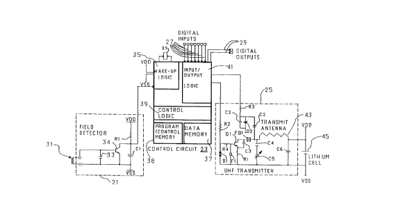
Turning to Figure 2, a representative transponder
or tag 3 is shown comprising~a detector 21 connected
to a control circuit 23 which in turn is connected to
a transmitter 25. As discussed above, an important
aspect of the present invention is the independence in
operation of the detector 21 and transmitter 25.
Specifically, the transponder or tag 3 is designed to
transmit an information signal via transmitter 25 upon
detecting the excitation field by means of detector
21. Yet, in accordance with the invention,
transmission of the information signal is independent
of sustained presence of the transponder or tag 3
within the excitation field.
Furthermore, the transmitter 25 according to the
present invention generates an information signal
imposed on a carrier frequency which is neither
derived from nor related to the frequency of the
excitation field sensed by detector 21, in contrast
.<-:~.~h the prior art systems described in European
~~a~.ent application 0, 253, 368 and United Kingdom patent
ap~ilications GB 2,202,981; 2,112,607; and 2,157,132.
In its basic form, the electronic circuitry of
the tag 3 is protected by a thin, resilient plastic
case, intended to provide protection against
accidental damage. According to a successful
prototype of the invention, the plastic case measures
less than 50 x 4o x 7 mm and weighs less than 20
grams. The case is sealed rendering it impervious to
the ingress of moisture and dust particles.
A plurality of digital inputs 27 are also
provided for monitoring the state of digital input
signals from external sensors such as temperature,
pressure, or simple switches, and a plurality of
WO 91/17515 PCT/CA91/00147
12
:~i
control outputs 29 are provided (only two such outputs
being shown for convenience) for optional control of
external devices connected to the tag 3 (e.g. an LED
for confirmation of reprogramming, audible alarm
buzzer, etc.). These outputs may be actuated in a
predetermined manner under the control of the program
stored in the tag's control circuit, or alternatively
following receipt of an instruction from the reader 1.
The sampled input information is reported to the
reader as part of the information signal transmitted
via transmitter 25. According to this feature,
additional applications of the identification system
may be provided without re-engineering the circuits at
the heart of the identification system.
The tag 3 is shown in greater detail with
reference to Figure 3 comprising a receive antenna 31
forming an inductive loop connected in parallel with
a capacitor 33 for forming a parallel tuned circuit
with a resonant frequency of approximately 135
kilohertz. The receive antenna is connected to
detector 21. Upon entering the excitation field
generated by the reader 1, the detector 21 senses the
presence of the field and in response generates a
carrier detect signal to wake-up logic circuitry 35
associated with the control circuit 23. Internal data
memory 37 of control circuit 23 stores user definable
information and identification data which is encoded
into an information signal by means of control logic
39 and then output to the transmitter 25 as a
modulation control signal via input/output logic
circuitry 41. Operating software for the tag 3 is
stored in a program (control) memory 38. The
transmitter 25 is enabled by.means of a power control
signal also received from input/output logic 41 under
control of logic circuitry 39 and in response
transmits the required information signal by means of
a transmit antenna 43, in a well known manner.
WO 91/17515 PCT/CA91/00147
:~ 13
According to an important aspect of the present
invention, an onboard power source is provided in the
form of a primary cell such as the lithium cell 45
having a nominal terminal voltage of 3V, and being
connected to control logic circuitry 39. The
provision of an on-board power source means that the
tag 3 is not required to extract operating power from
the excitation field, in contrast with the prior art
system disclosed in United Kingdom patent application
GB 2,163,324. The control logic circuitry 39 monitors
the condition of the lithium cell 45 and reports the
amount of charge to the reader 1 in the transmitted
information signal along with the user specified data
contained in memory 37, such that the system
monitoring computer 17 is provided with an early
warning that the tag 3 is nearing the end of its
useful life, and will therefore require replacement.
In operation, the tag 3 remains in a dormant or
quiescent state when it is out of range (e. g. more
than 3 meters away) from the excitation antenna 7 of
reader 1. In the idle state, the tag 3 consumes
negligible power from the lithium cell 45, and
transmitter 25 is down-powered by the control circuit
23.
The excitation antenna 7 is driven by transmitter
5 for generating a localized electromagnetic field
which is detected by the tag 3 by means of antenna 31
and detector circuit 21. In response to detection of
the electromagnetic field and generation of the
carrier detect signal by detector circuit 21, wake-up
logic circuitry 35 enables the control logic 39 to
retrieve the necessary user specified data in memory
37 and enables input/output logic circuitry 41 to
generate the required information signal for
transmission via transmitter 25. As discussed above,
the control circuit 23 also monitors the charge state
of lithium cell 45 by briefly enabling an on-board
WO 91/17515 PCT/CA91/00147
14
micro-power voltage comparator (not shown), and
responsive to the result of comparison generating a
status bit for inclusion in the transmitted
information signal.
Unlike prior art transponder identification
systems, the tag 3 of the present invention is
programmed such that it requires only a very brief
excitation signal for enabling it to transmit the
information signal. This aspect, coupled with the use
of an efficient UHF transmitter 25 eliminates the
necessity in prior art systems of requiring the
sustained presence of the excitation signal for the
duration of transmission of the information signal.
Consequently, it is possible according to the present
invention to identify objects which are moving at a
high speed relative to antenna 7, without requiring
the antenna 7 to be of unmanageably large dimensions.
According to the preferred embodiment, the tag 3
stores up to 32 bytes of user specified data within
memory 37. Of course, the number of characters stored
is limited only by storage capacity of memory 37.
This data relates to information about the object to
which the tag 3 has been attached. The data is stored
in a "free field" format, which means that the data
may be interpreted in different ways according to each
application.'
The data stored in memory 37 is reprogrammable by
the user, by means of sending coded, modulated radio
signals to the tag 3 from the reader 1 via antenna 7.
Programming of the tags 3 does not require contact
with the reader 1 to perform this function.
Programming of the tag is initiated by generation
of a keyword signal by reader 1, followed by
programming instructions, and, if required, additional
user specified data. The tag 3 compares the received
keyword with a stored version of the keyword, and in
the event the comparison fails to match the keywords,
WO 91/17515 ~ ,~ , PCT/CA91/00147
E~
the tag 3 denies access to memory 37. In addition to
this first level of programming security, the reader
1 and tag 3 may exchange instructions and responses in
a rigidly defined "hand-shake mode" such that if this
5 mode is not followed, the tag 3 will again refuse
access to the memory 37.
It is possible to write protect the tags 3 by
incorporating a "read only flag" associated with the
control logic circuitry 39 for rendering the tag 3
10 effectively "read only" such that it may not be
reprogrammed by the user. The read only flag is
analogous to a read only attribute appended to a file
stored on a computer disc according to well known
prior art.
15 After programming data has been sent to the tag
3 for storage in memory 37, the reader 1 may assert
the read only flag such that the tag 3 will thereafter
not allow the data stored in memory 37 to be altered.
However, this protection may be removed by an
instruction generated by the reader 1 for over-writing
the write protection.
The tag 3 may also be programmed to generate a
unique (characteristic) information signal upon egress
from the excitation field so that the reader 1 is
notified that the object bearing the tag has exited
from the field of influence of the excitation signal.
In order to accommodate different applications,
the identification system of the present invention is
designed to form a turnkey system for an end user.
For example, in a personnel identification system it
is a prerequisite that many tags 3 can be identified
at the same time - simultaneous identification -- yet
the identification process can be relatively slow
(e.g. 100-200 milliseconds). In contrast with the
personnel identification application, identification
of a fast moving object such as a car will typically
not require simultaneous identification. Thus, each
WO 91/17515 PCT/CA91/00147
A~16
tag 3 can be configured to optimize its performance
for any applications by simply programming the tag 3
with special instructions via the reader 1. Table 1
lists the programmable variables for the tags 3 which
may tailor the
be modified
by the
reader
1 to
performance individual
of the
system'
to each
application.
TABLE
1
Paraascer
~
' i to 3Z
~ Number
of data
bytes
transmitted
Der
messa~~
~ Mlabsr 1 to 15 V
of initial-
asssese
trensaissioas
is~sdiately
i
a tollo~in~ o
dstsction
of the
excitation
signal
I
i Delay
betnsa i
detection
of the
excitation
sisnal
and
w transmission 1 to 15 d
of initial
~essase
packsts.
Measured
i
r a a ;
siultiple
of a
sit~le
s~sssa~e
duration
i
1 5 w lnten~al beteeen nessade transaissions w
subspuent to i
initial s~sssase traosaissions. s~sasured 1 to Zs0
as a sultiple h
~ n
of a
sin=1e
~sssate
duration
Auaber 0 to Z53
of repeated a
sit~le
aessa~e
transaissions
after
i
r trans~ission or uali~ited
of set a
au~ber
of initial
wssa~es
i
Transmit data rate ( bits per second
) j 4800 to 38400
2 0 first node (sand sat nuaber of aessases tolloefw~ ~ d
detection o! xbe excitation sipal. reprdless o!
pceseacs or absence of that siprel) j Yes or no
ic~ypt data prior to tranwission
yes or no
-h
Ilrite protect nser-data
j yes or ao a
~ Tran:aitted data foaott sync or async
As can be seen from Table 1, some notable
features of the present invention include initial
pseudo-random delay, variable interval between
successive retransmissions, variable number of retries
and data encryption prior to transmission. The
features of initial pseudo-random transmission delay,
variable interval between successive retransmissions,
and variable number of retries are used to accommodate
simultaneous detection of information signals in
applications such as personnel identification.
WO 91/17515 '~ ~ ~' PCT/CA91/00147
17
Simultaneous detection of information signals
from numerous transponders is known in the prior art.
Some systems, such as those disclosed in United
Kingdom applications GB 2,202,981 and GB 2,157,132 use
sophisticated polling schemes in order to resolve
contention between transponders competing for a single
channel communication link to the reader or
interrogator. However, such prior art techniques
suffer from the disadvantage of requiring two-way
(i.e. bidirectional) communication between the
transponders and reader in order to achieve this
objective, thereby reducing the speed of arbitration
and hence degrading the relative speed of movement
accommodated between the transponders and reader.
However, in practice, only a limited number of
transponders (i.e. objects to be identified) can be
accommodated within range of the excitation signal
generated by the reader. This physical limit
determines the maximum number of transponders which
can be identified simultaneously. According to
the present invention, as discussed above with
reference to Table 1, each transponder or tag 3 can be
programmed to delay its initial transmission by a
variable amount, such that the likelihood of another
transponder or tag 3 broadcasting at the same time is
reduced. Hence, the likelihood of the signal from one
tag 3 being received uncontested is substantially
improved. This initial signal delay technique of the
present invention does not require communication from
the reader 1 to the transponder during the
identification process and therefore does not
significantly extend the length of the time required
to identify several transponders.
In some applications, where it is known that the
tags 3 will remain in the excitation field for a
considerable period of time relative to the length of
time taken to receive an identification message, it
WO 91 / 17515 PCT/CA91 /00147
I~ 18
may be desirable to ensure that the tags 3 fall idle
once identified and do not transmit further
identification messages, thereby clearing the
communications channel to the receiver 11 of reader 1
for use by other tags 3 entering the excitation field
at a later time. The tag 3 0~ the present invention
supports this function by means of programmability to
offer a set number of retransmissions whilst it
experiences a continuous excitation signal from the
reader 1, thereby giving a further improvement to the
simultaneous identification performance of the system.
In addition, the value of the retransmission interval
stored in a tag can be extended by a pseudo-random
amount so that the period between a pair
retransmissions (e. g. Ri and Ri+1) is different than
the period between the retransmissions Ri+1 and Ri+2.
This simple technique effectively results in the
ability to accommodate an unlimited number of tags 3
in the field of influence of the excitation signal,
and each tag 3 entering the excitation field will be
quickly identified without recourse to a complex two-
way communication scheme as discussed in the prior
art.
The use of keys for encryption and decryption is
also well known in data encryption communication
systems (e.g. military radio systems). According to
such systems, the key is changed in a random fashion
and applied to messages prior to transmission and on
reception. The value of the key at any time is known
to both the transmitter and receiver, and the
algorithm under which the key is changed, and the
encryption and decryption algorithms are also known to
both the transmitter and receiver. Thus, once
synchronization is achieved between the receiver and
transmitter (e. g. the key is set to an initial value),
the key can then be changed frequently and without
making the key publicly known. This prior art type of
WO 91/17515 _ PCT/CA91/00147
19
system assumes that there is considerable intelligence
in the form of a powerful microprocessor in both the
transmitter and receiver.
Encryption has been applied to transponder
identification systems as well. The broad ranging
applications for identification transponders means
that a tag might hold information in its memory that
is either of itself sensitive, or the tag may be used
for security access control purposes. In either case
the system would benefit from an added degree of
protection for the information transmitted by a tag,
such that firstly the actual information contained in
data patterns transmitted was not obvious, and
secondly that electronic eavesdropping using
sophisticated equipment to receive, reconstitute and
re-broadcast a transmission would not, in the case of
a security application, grant access to secure areas
or information. The schemes devised for the current
invention gives both facilities to the system.
One approach is disclosed in United Kingdom
application GB 2,202,981, in which a key is broadcast
to the transponder by the reader, which the
transponder uses to encrypt its stored data prior to
transmission. This approach suffers from the
principal disadvantage that there is the requirement
of two way communications between the reader and
transponder, since the reader must give the key to a
transponder in order that an encrypted message may be
formatted and broadcast. This in turn means that the
relative speed of movement between transponder and
reader is reduced by comparison with the simple
excitation/response sequence of the present invention,
as discussed herein above.
In accordance with an additional feature of the
present invention, data encryption is provided without
the requirement to pass a key from the reader 1 to the
transponder 3. Specifically, according to the
WO 91/17515 PCT/CA91/00147
invention, the tag 3 generates the encryption key
itself, using a defined algorithm, such that the key
varies in a pseudo-random fashion with a very long
cycle length. The key is then used to encrypt the
5 data stored in memory 37 prior to transmission.
However, in order that the reader 1 can make use of
the information and apply the correct key in order to
decipher the received information signal, the key is
embedded in the broadcast information signal from tag
10 3.
In the reader 1 of the present invention, a
specific location is reserved in the memory of
microcontroller 13 for storing the last received value
of the encryption key. Subsequent transmissions by
15 the same tag 3 will report a different key value. The
reader 1 qualifies a received message by inspecting
the last value of the encryption key associated with
a particular tag 3, and if the key is different from
the newly received value, then the message is regarded
20 as valid whereas, in the event the keys are identical,
the information signal is rejected (e.g. the bearer of
the tag 3 would be denied access in a personnel
identification system). This scheme prevents the
recording and replay of a signal transmitted by a tag
in an attempt to breach the security of the system,
since the second (false) transmission will be treated
as invalid by the reader.
Figure 4 shows the typical character and message
composition for information transmitted by tag 3.
Specifically, Figure 4a shows an asynchronous
serial frame, comprising a start bit (S), eight data
bits (DO-D7) , and a stop bit (P) . The start bit is
always logic 0 polarity, and the stop bit is always
logic 1. The data bits may be of either state. The
start bit is transmitted first (in time) and the stop
bit last. The duration of each bit is the same. This
is a standard format used in serial data
WO 91/17515 PCT/CA91/00147
..
21
communications between computers and peripherals. The
UHF receiver 11 of the reader 1 commences sampling
with respect to the leading edge of the start bit, the
validity of which is qualified by sampling the state
of the start bit at its nominal centre in order to
eliminate false start bits caused by noise in the
reception channel. Each data bit is sampled at its
nominal centre, so the accuracy of each bit period
need only be sufficiently good to ensure proper
sampling over the length of one frame. Hence there is
no need to provide a self-clocking modulation scheme
with this type of frame format. By way of example,
the practical implementation for this type of coding
is effected in the preferred embodiment of the present
invention by means of a frequency modulated
transmitter 25 (Figure 3), such that one logic state
(logic 1, say) is transmitted at a frequency [fo+f,],
where fo is the fundamental frequency of the
transmitter s reference oscillator, and the change in
frequency caused by taking the modulation control
signal from logic 0 to logic 1 is 2fa. In this
practical example, a frequency shift keyed (FSK)
modulation scheme is implemented.
Figure 4b shows a synchronous serial frame, which
comprises just eight data bits (DO-D7). Unlike the
asynchronous frame there is no start or stop bit.
Like the asynchronous frame, data bit DO is
transmitted first (in time) and D7 is transmitted
last. The synchronous frame format is also widely
used in computer communications. Unlike the
asynchronous frame format, synchronous transmissions
require either that the frequency of the transmit
reference clock and receiver sampling clock are very
closely matched, or (and more commonly) that a self-
clocking scheme is employed. Using the above-
mentioned FSK modulation scheme, it would be preferred
that each data bit was represented by a portion of the
WO 91 / 17515 PCT/CA91 /00147
22
upper transmission frequency [fo+f,] and a portion of
the lower transmission frequency [ fo-f,] . An example
of a practical scheme would be to use a so-called
Manchester encoded scheme, where each bit of a
character was transmitted such that the first half of
a bit was transmitted at [fo+f,j and the second half of
the bit was transmitted at [fo f,] if the state of the
data bit was logic 1, or [fo f,] followed by [fo+f,] if
the state of the data bit was logic 0. Hence the
receiver can extract a clocking (sampling) signal on
a bit-by-bit basis, thereby maintaining sampling
timing accuracy of the message length.
As described herein above, one programmable
feature of the present invention permits the tag 3 to
transmit its stored data in either of these formats,
character by character, with the speed of transmission
(the bit period) also being programmable to match
standard data communications speeds.
Figure 4c shows a string of "n" characters, each
composed in an asynchronous serial frame. There may
be any number of characters between character "a" and
end character "n". It should be noted that there is
not of necessity contiguity between successive
characters, and the interval between character frames
may vary. The interval between character "b" and
character "n" is filled with other characters, with
intervals between those characters which may be
variable.
Figure 4d shows a string of "n" synchronous
character frames, composed to form a synchronous
character string. It should be noted that there is no
interval between successive characters in this mode,
and that the interval between character "c" and
character "n" in Figure 4d is an integer multiple of
the time taken to transmit one character and will in
practice be filled with contiguous character frames.
WO 91/17515 PCT/CA91/00147
23
Referring now to Figure 4e, a message composition
is shown which is independent of the frame format and
method of modulation. Each character "a" to "n" is
either an asynchronous character frame or a
synchronous character frame, and each block in Figure
4e which represents a single character frame is deemed
to include any framing (start and stop) bits present
(in the case of an asynchronous frame format).
It is a programmable feature of the present
invention that the length of a message comprising "n"
character frames is variable; that is "n" is a
programmable variable. As discussed herein above, the
information stored in the tag's data memory 37 is held
in a "free-field" format, which means that the
contents of the memory is variable and open to
interpretation which will depend upon the application
of the tag. That is to say the user of the system can
store in the tag's memory 37 any information, held in
8 bit frames, so that it is quite practical to store
in locations for characters "a" and "b" two
synchronization characters which are required to allow
a receiver operating in a synchronous reception mode
to discern the start of a message from a tag, for
example. Similarly error checking information would
typically be transmitted in character positions "n-2",
"n-1", with a closing flag in position "n" in
accordance with a standard synchronous data link
protocol.
Furthermore, as discussed herein above, it is an
additional feature of the present invention that tag
3 may be configured to apply an encryption algorithm
to the data stored in its memory 37 prior to
transmission, and that in the scheme devised the
encryption key is included in the message transmitted
by the tag. The encryption key is embedded in a
transmitted message in a location known to the reader
WO 91/17515 PCT/CA91/00147
24
t.,
1 (which may be variable), so that the reader may
decipher a received message which has been encrypted.
Additional structural and operational details of
the tags 3 are provided below with reference again to
Figure 3 of the drawings, comprising a current best
mode of the invention. Of course, additional modes
and embodiments are possible within the scope of the
present invention.
Field Detector 21
Low frequency signal receiver 21 comprises a
ferrite cored inductor 31, which is brought to
resonance at the frequency of the excitation signal,
by parallel tuning capacitor 33. The output signal
from this tuned circuit is applied to the base of a
transistor 34. Sufficient bias current flows into the
base of transistor 34 to cause it to conduct when the
voltage developed across the tuned circuit exceeds
approximately 600 mV. The collector of transistor 34
is connected to an amplitude demodulator comprising
resistor R1 and integrator capacitor C1, so that a
signal detected by antenna 31 will cause a signal to
be passed to the control circuit 23 indicating the
presence of an excitation signal.
Control Circuit 23
The control circuit 23 in this practical example
is an 8-bit CMOS microcontroller and comprises mask-
programmable ROM (program memory 38), RAM (data
memory 37) a timer and data processing circuitry
(control logic 39), input/output ports (input/output
logic 41), and operating mode control logic (wake-up
logic 35). It is continuously powered from the
lithium cell 45 which has a nominal terminal voltage
of 3V (for a lithium manganese-dioxide cell). Control
circuit 23 derives its internal timing from an on
board oscillator, which has a ceramic resonator X1 as
its frequency determining element.
25
Whilst the tag 3 is remote from the influence Of the
electromagnetic field generated by the transmit antenna 7
of the reader, the tag is in a quiescent stage, in which it
consumes minimum current from its lithium cell 45. The
. control circuit is in a "sleep" stage, with its oscillator
and the UHF transmitter 25 disabled. In this "sleep" mode,
the control circuit 23 is responsive to a logic low signal
from the field detector circuit 21. When the voltage on
the collector of 34 goes low, the control circuit is
brought out of the sleep mode and its oscillator is
restarted. During the short period whilst the oscillator
is stabilizing, the control circuit is prevented from
executing instructions by internal logic. The control
circuit 23 will power-up and enable the UHF transmitter 25
periodically, and produce response signals by applying
modulation control signals via an output pin. The
composition of the data and the rate at which it is
presented via the modulation control line is determined by
the information stored in the data memory 37 of the control
circuit.
When the tag 3 no longer experiences an excitation
signal detectable by the field detector 21, the voltage on
the collector of 34 rises, and the control circuit may stop
transmission of response signals, then place itself in a
sleep mode ready for detection of the next excitation
signal. It may be that the control circuit 23 has been
programmed by instructions from reader 1 to ignore the
state of the signal from the field detector circuit 21
until it has completed transmission of an identification
message or messages, in which case there will be a delay
between the collector of 34 going high and the cessation of
transmissions by the tag 3.
. 35 During the period immediately following cessation of
transmissions by the tag 3 and after removal of the
51,1~~~'t~'~ ~ ~ ~'-~~T ~.
WO 91 /17515 PCT/CA91 /00147
,... 2 6
excitation signal, the control circuit 23 will monitor
the output from the field detector circuit 21 or
modulations which might have originated from reader 1,
since this is the method of communicating instructions
and data to the tag 3. If correct modulations are
detected, the control circuit 23 enters a receptive
mode in which it will monitor the carrier detect line
for further modulated signals. Properly coded signals
will cause the control circuit 23 to accept data for
storage in its data memory 37 for subsequent
transmissions.
UHF Transmitter 25
The UHF transmitter 25 is essentially an
oscillator with Q1 as its active element, which is
designed to radiate a very low level of signal through
transmit antenna 43, which may for convenience be a
profiled track on the printed circuit board (PCB) on
which the other components of the tag are mounted.
Modulation may be applied to the oscillator which
causes the frequency of oscillation to vary slightly,
thereby allowing transmission using a frequency shift
keyed (FSK) system.
The circuit 25 comprises high frequency
transistor Q1, which has an inductive collector load
in the form of a PCB track, with feedback capacitor C3
between collector and emitter to form a simple
Colpitts oscillator. The ferrite bead FB1 is included
since it presents an impedance which rises very
sharply above the fundamental frequency of the
oscillator, thereby significantly reducing the
harmonic distortion in the output signal. The
fundamental frequency of this oscillator is determined
by a surface acoustic wave (SAW) resonator F1.
The operation of the transmitter 25 is controlled
by the control circuit 23, the oscillator is enabled
by applying bias directly from an output pin via
resistor R2 to the base of Q1. When the control
WO 91/17515 ~ ~ ~ ~ ~ PCT/CA91/00147
27
(bias) voltage is high, the oscillator is enabled.
The base voltage is set by double diode D1 and is thus
independent of the supply voltage. When the bias
voltage is low, the oscillator is disabled, and the
circuit consumes negligible current. The output from
the oscillator is peaked by variable capacitor C5,
which predominantly affects amplitude and to a much
lesser extent frequency.
Modulation is applied to the transmitter 25 by
applying a control voltage through resistor R3 to
diode D2, which, whilst not being a true variable
capacitance diode, exhibits a change in reverse
capacitance with applied voltage sufficient to alter
the impedance of the collector load circuit and pull
the frequency of the oscillator. This variable load
capacitance is coupled to the collector circ~:.y by
capacitor C2. A frequency modulation scheme is
thereby operated by the control circuit. Naturally,
a 100% amplitude modulated signal can be generated at
one of two frequencies simply by gating the base bias
on and off at the required rate.
Turning to Figures 5 and 6, a transponder
according to the preferred embodiment is shown
comprising signal receivers 51 and 52, a demodulator
53, a control circuit 54, frequency synthesizer 55,
transmit antenna 56 and a cell 57.
Detectors 51 and 52 are shown by way of example
as being low frequency and microwave detector
circuits, respectively. However, other frequency
specific detectors may be utilized.
Microwave detector 51 comprises a half-wave
dipole antenna in the form of strips on a printed
circuit board, radio frequency choke L3 and Schottky
detector diode D1. The energy detected is stored as
a charge on capacitor C4, and resistor R2 provides a
DC path to the reference level V" for diode D1. The
WO 91 / 17515 PCT/CA91 /00147
28
voltage developed across capacitor C4 causes bias
current to flow into the base of transistor Q2.
Low frequency signal receiver 52 comprises a
ferrite cored inductor L2, which is brought to
resonance at the frequency of the excitation signal by
parallel tuning capacitor C2. The output signal from
this tuned circuit is applied to the base of
transistor Q1. Sufficient bias current flows into the
base of transistor Q1 to cause the transistor to
conduct when the voltage developed across the tuned
circuit exceeds approximately 600 mV. The collector
of transistor Q1 is connected to the collector of
transistor Q2 and to the demodulator 53, so that
either a signal detected by a low frequency signal
detector 51 or by microwave signal detector 52 will
cause a signal to be passed to the control circuit 54
indicating the presence of excitation signal.
In common with the transponder discussed above
with reference to Figures 2 and 3, various
programmable features are provided and the operation
of the transponder may be modified by modulated signal
programming.
In the preferred embodiment illustrated,
amplitude demodulator 53 comprises a resistor R1 and
a capacitor C1. Either transistor Q1 or transistor Q2
is capable of clamping the voltage on the integrator
capacitor C1 in order to indicate the presence of an
excitation signal to the control circuit 54.
Circuit 54 controls operation of the transponder.
In the absence of a signal from the demodulator 53,
the control circuit 54 is in a quiescent state. The
control circuit down powers the frequency synthesizer
55, and places itself in a mode where it consumes
least current. The control circuit 54 exits the
quiescent state in response to detection of an
excitation signal. According to the preferred
embodiment, control circuit 54 is manufactured as a
WO 91/17515 PCT/CA91/00147
29
custom-designed integrated circuit fabricated in CMOS
technology. Alternatively, the control circuit 54 can
be in the form of a mask programmed 4 or 8 bit CMOS
micro controller, such as the 84C00 family of micro
controllers manufactured by Philips Components, such
a device containing the functional blocks shown in
Figure 5 necessary to control the operation of the
transponder, including a data memory where
identification data may be stored.
The control circuit 54 manages the operation of
the frequency synthesizer 55, via the clock and data
lines shown, by passing data to be transmitted via the
modulation control line, and is able to place the
synthesizer in a powered-down state by actuation of a
power control signal.
Frequency synthesizer 55 comprises principally a
crystal controlled reference oscillator and a digital
phase locked loop which acts to produce frequency
multiplication, and includes a voltage controlled
oscillator. A detailed description of the elements of
the frequency synthesizer is not provided herein, as
the design and principles of operation of such devices
are well known in the industry. For example, a well
known frequency synthesizer is the UMA1014
manufactured by Philips Components.
As discussed above, the control circuit 54
provides instructions to the frequency synthesizer 55
viG the clock and data control lines, including the
setting of the transmit frequency. Modulation is
applied to the frequency synthesizer 55 from control
circuit 54 via the modulation control signal line.
This modulation may affect the amplitude, frequency or
phase of the transmitted signal, which is propagated
by transmit antenna 56 for reception by a receiver
which is tuned to the transmission frequency of the
transponder.
WO 91/17515 PCT/CA91/00147
The manner in which the transponder is
programmed, for example to direct the control circuit
54 to pass an instruction to the frequency synthesizer
55 to select a particular response frequency, is
5 discussed above in greater detail.
The transponder circuit is powered by a small
primary cell 57, which may use lithium-manganese
dioxide or lithium-thionyl chloride chemistries, for
example.
10 In summary, according to the present invention,
an identification system is provided in which
sustained presence of the tag or transponder is not
required for transmission of an identification
information signal. Independence between the receiver
15 and transmitter of the tag permits transmissions of
data at standard rates and with standard formats, and
permits the concepts described to be applied to any
system independent of the frequencies of operation.
Additional powerful features such as data encryption
20 and the programmable characteristics of the tags
described are features in isolation and not reliant
upon the separation between receiver and transmitter.
Other embodiments and variations of the present
invention are possible within the sphere and scope of
25 the claims appended hereto.
For example, the number of signal receivers-
detectors in the preferred embodiment of Figures 5 and
6 need not be limited to only two as shown.
Theoretically, an unlimited number of excitation
30 signal receivers can be employed allowing the
transponder to be excited by a wide range of
excitation frequencies. An alternative implementation
could use a signal receiver which scans across a range
of frequencies.