Note: Descriptions are shown in the official language in which they were submitted.
WO 92/00643 PCl`/CA91/00202
hINE IN~ERFACE CIRC~IT
Introduction
The invention is in the field of telephony and
more particularly relates to interface circuits for
supplying energizing current from a power source for
operation of a telephonè set, via a teleph~ne line, and for
coupling signals between the telephone line and a telephone
10 facili~y.
~a~k~rou~d of th~ Inventio~
One o~ the major expenses in a telephone system is
15 that of providing a line interface circuit for connecting
each and every telephone line at a central office switching
facility, or àt a private branch exchange facility. In any
practical telephone system, the line interface circuits are
desirably inexpensive and essentially electrically robust.
20 During those times when a telephone set is in use, the
associated telephone line ~ ace circuit provides an ;~
~; energizing direct current for the telephone set, via ~ip and
ring leads of the telephone line. When the telephone set is
in use, i~ is usually referred to as being OFF HOOK, and
25 when the telephone set is not in use, it is referred to as ~ -
being ON ~OOK. The line interface circuit is also required
to provide indication as to the telephone set being ON HOOK
or OFF HOQK.
A source of ~he energizing current is usually a
30 central battery supply. The central battery supply is
continually charged to a predetermined voltage by a battery
charging apparatus, provided for that purpose. The ba~tery
charging apparatus is operat~ed from utility power, ~ut in
the event of an interrupcion of the utility power the
35 central battery supply is intended co continue to supply
operating current for a limited~time. The battery charging
appara~us of~en~includes a switchin~ invertor, which as a by-
product of its operation, genera~es elec~rical noise.
~Typically one of the functions of the line circuit is ~hat
' :~
WO9~/00~3 P~T/CA91/00202
2~ 3 `'
of preventing noise signals of any origin from traversing
the co~nection between the central battery supply and the
telephone line. For example, in the Unieed States, Patent
No. 4,103,112 issued on July 25, 1978 to V.V. Korsky, and
5 titled ~Telephone Line Circuit With Differential Loop
Current Sensing And Compensation~, a telephone line is
terminated at tip and ring terminals connected to tip and
ring windings of a transformer. ~nergizing direct current
ls conducted by 200 ohm tip and ring feed resistors
10 connected in series between the battery supply and the tip
and ring windings. A 2.16 microfarad capacitor is connected
between the tip and ring windings. The capacitor provides
an impedance path for alternating current voice band
siynals, whereby very little of the signal energy is
15 dissipated across the feed resistors.
The value of the capacitor is essential in
determining the terminating impedance of the line circuit.
In United State~ Patent No. 4,864,60g, issued on September
5, 1989 to M.S. Moisin, and titled ~Telephone Line Interface
20 Circuit'~, a compensating circuit for adjusting the val-ue of
the operating terminating impedance to more closely approach
the value of a predetermined preferred terminating
impedance, is discussed. ~he compensating circuit is
connected to drive a winding, in the transformer, in a
25 current opposing relationship with respect to some of the
di~ferential alternating current signals in the tip and ring
windings. The differential alternating current signals
specifically referred to are those within a lower portion of
the voice frequency range, for which an impedance of the
30 capacitor is significantly shunted by the feed resistors.
United States Patent Nos. 4,764,956, issued 16
August 1488 to R. Rosch et al; 4,514,595, issued 30 April
1985 to S. Rosenbaum et al; 4,484,032, issued 20 November
198g to S. Rosenbaum; 4,539,43g issued 3 September 1985 to .
35 S. Rosenbaum et al: 4,532,381, issued 30 July 1985 eo S.
Rosenbaum et al and 4,571,460 issued 18 Februar~ l9B6 to S.
Rose~baum et al are each concerned with providing the
required terminating impedance via active circuit apparatus.
Particularly, ~ip and ring amplifiers are controlled in
' ' '
: ."~ "
.. ...
3/l
response to direcc loop cu~~e~t and al~ernating di, e-en~ial
current signals detec~ed across ti~ and ring feed resisto-s,
to generate the terminating impedance and to injec~
alternating current signals fo~ t~ansmission via the
5 tele~hone li~e to the t_le~hone set. The de~ec~e~ line
! cu-ren~ is also used 25 a source of al-~e-nating curren~
signals for transmission to a hy_~id circuit wherein signals
from the telephone se~ ar~ transmitted via the associated
telephone facility. In Euro~ean publication number
10 A, 0022501 the a.c. sig~al functions of the tip and ring
amplifiers are performed by a single amplifier which is
transformer coup'ed to res?ec_ive tip and ring windings.
The amplifier is controlied in response to current sic3nals
detected across ti~ and ring feed resistors in a mann2r
similar to that previously discussed .
The performance of these types of line inter,~ace
circuits is adversel-y affsctê~ by practical limitations o~
common mode rejection c;~arac.eristics o- analog different-lal
am~lifier circults. These characteristics may be
significantly compromised in the interest of economy, b~
integra~ion or the analog dlf-e-ential amplifiers along with
digi~al circuit elements, essential for pulse code modulated
time division multiplex inte--ace with the associated
telephone facility. These charac-eristics may be further
2s compromised if either of the ~i~ and ring feed resistors
becomes mismatched. For example, during use of a line
interface circuit, one of the tip and ring feed resistors
may age in response to unusual s_~ess, as may accompany a
trahsient elec~rical event su_h as a p^wer line cross or a
lightning strike in association with the telephone line.
'-'. :~.' '
Summary of the Invention
::
The invention is a line-interface circuit for
supplying energizing current from power terminals to a two
wire communication line and for coupling communications
signals between the communication line and a telephone
~ ~ g~5~
3/2
facility via a hybrid circuit means. The line interLace
circ~it includes tip and ~ing terminals for connection to
the two wi-e communication line and h~3rid .ransmit and
receiv_ te~minGls for connection to the hy~-id circuit
means. .~ ~ip and ring signal vol~age detecror, is
respor.sive to dirLerential signals appearing across the tip
and ring terminals and to signals appearing at the receive
terminal, for generating a composite signal. A loop driver
'' ', ',
,/
.
/: .
,i '~" ,.;,
.,,~'. ,
- :.
-
".,, ;'~ .
,-.
. :...
.~, . '
', ' '
,'
''' ;.'~'"
. :.,-::-:
sUBS~UT~S~
.: .
W092too~3 2~ ~ 3 PCT/CA91/00202
~ 4 ~i
circuit is co~nected in series between the power terminals
for supplying the energizing current, and is responsive to a
control signal for driving alternating current signals via
the tip and ring terminals. A loop current detector is
5 connected in series between the tip and ring terminals and
the loop driver circuit, for generating a line signal in
response to current flow in the communication line. A
network includes a first port being connected to receive the
composite signal from the tip and ring sicJnal voltage
10 detector, a second port being connected to receive the line
signal from the loop current detector, and a third port
being connected to the loop driver circuit for providing the
control signal.
In one example or the line interface circuit the
15 network comprises a reactive impedance means, including a
capacitive device and a resistive device, being connected
between the first and third ~orts, and a resistive impedance
means being connected between the second and third ports.
one of the capacitive and resistlve devices comprises a
20 plurality of impedance elements and a corresponding
plurality of switches. Each of the switches is connected in
parallel with one of the impedance elements. Each of the
switches is controllable to be in an OFF state whereby the
value of the associated impedance element appears across the
25 switch, and to be in an ON state whereby a value of less
than the value of the associated impedance element appears
across the switch. Each of the impedance elements is
connected within a predetermined pattern in series between
the first and third ports, whereby the characteristics of
30 the network may be changed by changing the states of
individual ones of the switches.
3rief Description of the Drawings
Exampie embodlments are discussed with reference
to the accompanying drawings in which:
Figure ' is a block diagram of a line interface
circuit in accordance with the invention;
,-
"'', '
Figure 2 is a schematic dlagram of an example
implementation of the line interface circuit illustrated in
figure l;
Figure 3 is a schematic diagram of an alternate
example of a loop current detector which may be used in the
line interface circuit illus~rated in figure l;
Figure 4 is a schematic diagram of an alternate
example of a loop driver circuit which may be used in the
line interface circuit illustrated in figure l;
o Figures 5 and 6 are schematic diagrams of examples
of variable components which may be used in any of the line
interface circuits illustrated in the preceding figures; and
Figure 7 is a schematic diagram of another alternate
example of a loop current detector which may be used in the
line interface circu.it illustrated in figure 1.
Description of the Preferred Embodiment
The line interface circuit illustrated in figure 1
20 includes tip and ring terminals 2 and 3 for connection to -
the tip and rlng leads of a telephone line (not shown),
power -V and ground GR~ terminals for connection to a
battery supply (not shown) and transmit and receive leads TX
and RX for connection to an electronic hybrld circuit (not
shown). Some of the signals appearing at the transmit lead
Tx are destined for an assoclated telephone facility (not
shown), and are selected by the electronic hybrid circuit
for transmission into the telephone facility. Signals -~ ~;
appearing at the receive lead ~ from the hybrid circuit,
are destined for transmission via the tip and ring terminals
2 and 3, to the telephone~llne.
In the line interface clrcuit, a tip and ring signal
voltage detector 20 ls responslve to differential signals
appearing across the tip and ring terminals 2 and 3 for
generating a corresponding single ended signal. The single
ended signal and the receive slgnal are used to provide a ~i~
; composite signal which is fed to a flrst port ~7 of a
network 40, and which is supplied to the electronic hybrid
circuit via the transmit lead TX. A loop current detector
~, ~
30 is connected in series between a loop driver circuit 50
and the ti~ and ri.ng terminals such that all of the current
flowing along a telephone line via the tip and riny terminals
2 and 3 also traverses the loop current detector 30. The
loop cu-rent detector 30 is responsive to differential
current flowing via the tip and ring terminals for generating
a line signal which is useful in an associated telephone
facility for detecting ON HOOK and OFF HOOK conditions. The
line signal is also supplied to a second port 48 of the
o network 40. The composite signal and the line signal combine
in the network 40 to provide a control signal a. a third port
49 of the network 40, which is connected to a loop driver
circuit 50. The loop driver circuit 50 connects the tip and
ring terminals 2 and 3 with the power terminals GRD and -V to
`' 15 provide a flow of energizing direct current for the operation
of a telephone set while it ls OFF HOO~. The loop driver
circuit 50 also drives alternating current signals via the
tip and ring terminals, such that the line interlace circuit
terminates the telephone line with a characteris~ic impedance
which substantially corresponds to a predetermined preferred
impedance. For example throughout North America, most
operating telephone companies require a terminating lmpedance
which is eouivalent to 900 ohms in series with 2.16
microfarads.
A detailed example of the line interface circuit of
figure 1 is illustrated ln figure 2. In the figures
generally, details of distributio~ of power, arrangements of
decoupling filters and biasin~ circuits are neither shown nor
described except where such m~y be beneficial, to a person of
typical skill in the elec~ronic ar;s, in understanding the
embodiments of the invention.
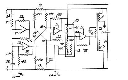
The tip and ring signal voltage detector 20 includes
a tip amplifier circuit and a ring amplifier circuit. The
tip amplifier circuit is provided ~y an ampli-fier 21 being
connected with resistors 22 and 23, and a capacitor 24, as
shown. The ring amplifier circuit is provided by an
amplifier 25 being connected with resistors 26 ancl 27, and a
capacitor 28, as shown. The capacitors 24 and 28 serve to
isolate the respective amplifiers 21 and 25
~ST3TUT~ SHl~
W092/00~3 PCT/CA91/00202
7 2~ 53
from DC potentials at the tip and ring terminals 2 and 3. A
resistor 29 is connected ~rom the output of the amplifier 21
to the input of the ampllfier 25 such that in combination
only differential signals appearing across the ~ip and ring
S terminals are reproduced at the output of the amplifier 25.
In this example the value of the resistor 22 is about a
tenth of the values of the resistors 23 and 27 to
substantially reduce any possibility of either of the
amplifiers 21 and 25 being driven into regions of nonlinear
10 operation by the presence of common mode signals, as may be
induced upon a telephone line by the influence of a utility
power line. Receive signals from the electronic hybrid
circuit and destined for the telephone line are coupled via
the receive terminal Rx, labelled 61, and a resistor 62 to
lS the input of the differential amplifier 25. The output of
the amplifier 25 is connected to the first port of the
network 40, and to the transmit terminal Tx, labellecl 6~.
The loop current detector 30 includes a resistor
network having a tip feed resistor 12, a ring feed resistor
20 13, each of which conducts virtually all of the currents
traversing the tip and ring terminals 2 and 3 respectively.
The feed resistors should be able to dissipate several watts
and have values of about ~00 ohms, and are usually matched
to within one percent of each other. The resistor network
25 also includes tip and ring voltage dividers 14 and 15
provided by resistors 14a, 14b, and resistors 15a and 15b
connected as shown to define tip and ring taps 16 and 17.
The values of the resistors 14a, 14b, lSa, and 15b are
usually matched to be withln plus and minus one percent of
30 each other. The tip and ring taps 16 and 17 are connected
across a differential input of a differential amplifier 31, - --
which is connected as shown in combination with resistors 32
and 33. The values of the resistors 32 and 33 are also
similarly matched to be within plus and minus one percent of
35 each other. Currents related to currents in the tip and
rlng feed resistors 12 and 13 are conducted via~the tip and
ring taps 16 and 17 and the resistors 32 and 33
respectively. Hence the differential amplifier 31 is dire~t
coupled to generate the previously mentioned line si~na;
'.. ~,:-.
, .
L ~:
W092/00~3 PCT/CA91/00202
8 :
which is representative of differential currents ~raversing
the tip and ring terminals 2 and 3. The line signal is
applied to a supervision lead 66 for use in the telephone
facility, and to a second port of the network 40 via a
5 capacitor 34. The capacitor 34 serves to isolate the
network 40 from a direct current potential at the outpu~ of
the amplifier 31.
The network 40 includes a resistor 42 and a
capacitor 4~ connected in series between the first and third
10 ports and a resistor 41 connected between the second and
third ports. This is to provide the previously mentioned
terminating impedance of 900 ohms in series with 2.16
microfarads. It has been found that in a lower portion of
the voice band, the preferred terminating impedance is more
15 closely adhered to if the RC values of the capacitor 24 and ;
the resistor 23 and the capacitor 28 and the resistor 27 are
about the same as the RC value of the capacitor 3~ and the
resistor 41. A resistor 43 is shown to be optional and is
required in those cases where an operating telephone
20 company~s standard line terminating impedance includes a
parallel resistance value.
In this example, the value of the resistor is
selected to be 900 ohms multiplied by a value x and the
value of the capacitor is seiected to be 2.16 microfaraas -
25 divided by the value x. The value of x may be determined as
~ollows:
The K1 represents a current-to-voltage transfer
function of the loop current detector 30, such ~hat
V1 = K1~T-R!
K2 represents a voltage-to-voltage transfer
function of tip and ring signal voltage detector 20, such
that
V~ = K~V~-R)
then, 1/x = ~l/RK- ie. x = RK,./K~
3~5 where IIT-R~ is differential line current and :
V!~^! is~differen~ial line voltage
In the example sh~n, R ~ 5 kilohms
..
! WO 92/00~3 ~ 53 PCT/CA91/OD202
.. 9
S mv~mA
K~ = 1.00
x = 200
The loop driver circuit 50 includes an amplifier
5 51 with an input connected to the third port of the network
0 and an output connected to a primary winding 6 of a
transformer 10. A feedback resistor 52 is connected between
the input and the output and is of a value selected to cause
the amplifier 51 to operate with a gain of about 100. The
10 transformer 10 includes a tip winding 4 connected in series
with the tip feed resistor and the ground power terminal
GRD, and a ring winding 5 connected in series with the ring
feed resistor and the power terminal -V. A capacitor 7 is
connected across the tip and ring windings 4 and 5 to reduce
15 electrical noises which may originate with battery charging :
apparatus. The windings are poled as indicated in figure 2
by conventional dot notation. In operation, energizing
direct current is driven along a path which includes the
power terminals and the tip and ring windings 4 and 5, which
20 are poled in a flux reinforcing direction. ~;
A sui~able transformer may be constructed to have
tip and ring windings of 376 turns each of number ~0
American Wire Gauge insulated copper wire and a primary
winding of 376 turns of number 42 American Wire Gauge
25 insulated copper wire. The windings are carried upon a
transformer core of ferrite material. one suitable core,
with identification ~EM6 has been found to be available from
Thompson Passive Components, 50 Rue J.P. TimbaudiBT13/92403,
Courbevoie, Cedx, France. Saturation by loop currents of up
30 to 100 milliamps is avoided by limiting the number of turns
in the tip and ring windings and by having a gap in the core
of the transformer of about 0.38 millimetres. In one
example of the line interface circuit component values as
listed herein below have been found to be satisfactory. ..
resistor 12, 13 180 ohms
a,l~b,15a,15b 120 kilohms -~
! ~.' :
Com~onent Value Units
22, 29 20 ~
23, 26, 27 200 "
32, 33 7.5 "
41 5
43 180 "
52 5 megohms
62 100 kilohms
capacitor 7, 24, 28 0.1 microfarads
34 A "
44 10.6 nanofarads
Referring to figure 3, an alternate example of a
loop current detector 130 is substituted for the loop
current detector 30, in figures 1 and 2. In other respects
figure 3 is consistent with the preceding figures. In this
example the loop current dete~ctor is provided by a hall
effect device 139, which is arranged to be sensitive to ~
differential currents traversing the tip and ring terminals ~ -
20 1 and 2. This ls accomplished by orienting the tip and ring -~
conductors such that common mode currents are of a magnetic
flux cancelling~effect, as shown. In operation the hall
effect device I39 generates an output voltage of a magnitude
corresponding to the flux intensity and of a polarity
corresponding to the direction of the flux. This
arrangement eliminates the requirement of a common mode
.
rejection characteristic in an on following amplifier. The
output voltage is conveniently amplified by an inverting
amplifier circuit shown at 139a.
30~ Refe~ring to figure 4, an alternate example of a
loop driver circuit 150 is substituted for the loop~driver
circuit 50,~in figures 1 and 2. Otherwise, the figure is in
accordance with the preceding flgures. In this example the
loop driver circuit 150 includes the amplifier 51 as in
35 figure 2, but the functions of the transformer 10 are :~
performed by ti~and~r}ng amplifiers 154 and 157. The~tip ;-~
amplifier 154 includes an lnput whi~h is coupled to the
output of the amplifier 51 via a resistor 153. The ring -
,, W092/00~3 ~~ .~J A PCT/CA9l/00202
11
amplifier 157 includes an input which is coupled to an
output of the ampl,ifier 154 via a resistor 156. circuit
values, as previously suggested for implementing the line
interface circuit illustrated in figure ~, may be
5 satisfactory for implementing the line interface circuit
illustra~ed in figure 4, providing that values of feed back
resistors 155 and 158 are chosen ~o operate the tip and rlng ,
amplifiers each with unity gain. For operation the tip and
ring ampliflers 154 and 157 are each connected to the
10 central battery supply via power terminals ~not shown). The
outputs of the tip and ring amplifiers may be connected as
shown to supply operating direct current and signals
destined for the telephone line to the tip and ring .
terminals 2 and 3, via the loop current detector 30, or via ,,'
15 the loop current detector 130. In view of the substitution
' of solld state amplifiers for the transformer 10, the line
,~ interface circuit of figure g, may be more economical to ~,.';,"
manufacture. Furthermore active tip and ring feed devices , ,~
such as the amplifiers 154 and 157 are readily adaptable to ,~. .
20 providing a feed current limiting function which is ': ''
advantageous on short subscriber loops which would normally ~-
draw in excess of 50 milliamps or so, for example, from the ;: '
central battery supply. However the line interface circuit ;.
may also be more vulnerable to transient events such as
25 lightning strikes. Hence lt may be advan~ageous to restrict
the embodiment of figure 4 to uses with loops which are :,:~ :
least likely to be SUDj ected to such events. .~'
The network 40 may include one or more integrated '~'
circuit resistive and capacitive devices which are variable ~ ,,
30 in response to digital control signals. Examples are shown ': -.
in figures 5 and 6. In figure 5 a resistive device includes ,,~ ,
resis~ors ~1 - R16 being connected in combination with : :
`. switch columns COL.0 - COL.15 each of which is uniquely
responsive ~o a digital con~rol signal applied at terminals '.,:,
3- A - D to provide a selected predetermined resistance value
across terminals 96 and 97. Each of the coiumns is provided ' '
by a combinac:ion of field efrect ~ransistors ~FETs),
directly responsive types being identified a' 92 with gate
electrodes 95 and inversely responsive ~ypes being
',..
,"'~,.
12
identified at 93 with gate electrodes 95~. The uni~ueness of
response of each column is determined by arrangements of
shorting conduc~ors as illustrated at 9~. In figure 6 a
capacitive device includes capacitors C1 - C16 arranged with
columns of abbreviated illustration but similar to those
shown in figure 5. The capacitive device is uniquely
responsive to a digital control signal applied at terminals
W -z, of which only terminal z is shown to provide a
selected predetermined capacitance value across terminals 98
and 99. These are exemplary of conveniently controllable
means by which the characteristic terminating impedance of
the line interface circuit may be selected subsequent to
manufacture to suit the re~uirements of a particular '
telephone company.
Another alternate detailed example of the line
interface circuit of figure 1 is illustrated in figure 7.
In figure 7, the tip and ring signal voltage detector is -~
provided by a differential amplifier 121, with inverting and
non inverting inputs being connected to the ring and tip
terminals 3 and 2 by series combinations of a resistor 127
and a capacitor 128, and a resistor 123 and a capacitor 124, '
respectively. A bias voltage VB is coupled to the non
inverting input via a re~istor 122b, and a feedback resistor ` ''
122 is connected between an output of the differential
amplifier 121 and the inverting input. Said output is also
connected via a resistor 129 to an input of an inverting
amplifier 125. An output of the inverting ampliEier 125 is
directly connected to a first port of a network 1~0 and a
feedback resistor is connected between the input and the
output of the inverting amplifier 125. Similar to the
example discussed in relation to figure 2j an output of an ;
electronic hybrid circuit, not shown, is connected to
provide receive signals, destined for the telephone line to -'
the input of the inverting amplifier 125 via the resistor '
62. Hence a composite signal, including components of the
differential signals on'the telephone line and receive
' s'ignal;s destined for the telephone line, is generated at the ' '
output of the inverting amplifier 125 and provided at the
~:
,~, .
13
Eirst port of the network 140 and at an input of the
electronic hybrld circuit.
A loop current detector includes a resistor
network having a tip feed resistor 112, a ring feed resistor
113, each of which conducts virtually all of the currents
traversing the tip and ring terminals 2 and 3 respectively.
In this example the feed resistors may be provided by
resistive elements, preferably having values matched to
within a half percent of each other. The resistor network
also includes tip and ring voltage dividers 114 and 115
having resistive elements with values being matched to be
within a half percent of each other. Tip and ring voltage
taps 116 and 117 are connected across voltage dividers 137
and 136. An inverting amplifier 135 includes an inverting
input being connected to a voltage tap 137a, a non inverting
input being connected via a resistor 138 to the bias voltage
VB, and an output being connected to a voltage tap 136a, as
shown. A differential amplifier 131 i.s connected with
resistors 132 and 133, as shown, with non inverting and
20 inverting inputs connected to the tip and ring voltage taps -: :
116 and 117 The ohmic values of the components shown in the : :
voltage divider 137 are preferably matched to within a few
percent such that in operation of the amplifier 135, most if
not all of any common mode signals as may be induced in or
otherwise coupled to a telephone line being connected at the
tip and ring terminals, will be substantially nullified, with
only differential signals being passed along from the tip and
ring voltage taps 116 and 117. ~
A network 140 is preferred to have a pass band ~ -
characteristic limited to the operating frequencies of
interest. The network 140 may include active components and ;
adjustable components as exemplified in the figures 6 and 5
and thereby be programable to be tailored to any specific
application. The network 140 includes resistors 146 and 145
which are shown externally in figure 7 for convenience of
discussion. Similar to;the network 40 discussed perviously,
the network 140 includes the first port connected to receive - ;
the composite signal, a second port connected to the output
of the amplifier 131 to receive a supervision signal, and a
.- . . .
third port for coupling a control signal from the network
1~0 to a buffered input of a loop driver circuit. In the
loop driver circuit,the buffered input is prov.ided by an
amplifier 161, hav:Lng a gain as determined by a resistor
162. A class AB current amplifier circuit 163 responds to
alternating current signals at the output of the amplifier
161, to drive the transformer 100 with alternating current
signals destined to be coupled to a telephone line via the
tip and ring terminals 2 and 3. The class AB current
amplifier circuit 163 includes a double rail output which is
connected to drive respective halves 106a and 106b of a
centre tapped primary winding in the transformer 100. Tip and
ring windings 104 and 105 in the transforrner 100 are
connected in series with the tip and ring terminals 2 and 3
as shown. It should be noted that in contrast to other
examples of the line circuit, in this example a current
limiter 109 is connected in series between the ring winding
105 and the talking battery terminal -V. The current limiter
109 is designed to be effective below the voice band to limit
energising direct current supplied via the tip and ring
terminals 2 and 3. The current limiter 109 is operative for
iexample in the case of the telephone line being a short loop
or in the event of a ground fault occurrence on the telephone
line. A damping network including a capacitor 107 and a
resistor 108 connected across the tip and ring terminals,
reduces any likelihood of unwanted oscillations which may
occur outside of the operating band of interest. The
particular embodiment of the invention as illustrated in
figure 7 has for purposes of efEicient production, been
30 realised to be advantageous. For example, use of the class ~ -
AB push pull amplifier 163 provides a driver circuit which
permits the transformer lOO to be of reduced bulk and
expense, relative to the transformer required for preferred -~
operation of the line interface circuit in figure 2.
Furthermore the use of a separate current limiter which
passes freqùencies of the voice band and greater permits a
further reduction of transformer bulk and also reduces the
maximum power dissipation requirements of the tip and ring
, ~ ,
PCTtCA91/00202
WO g2/00643
-: 15 2~ 3
îeed resistors. In the example of figure 7, a suitable
transformer may be constructed upon a powdered iron core
#E13-40 available from Micrometals Inc., 1190 N. Hawk
Circle, Anaheim, California 92807-1788. The core carries
5 tip and ring windings of 600 turns each of number 38
American Wire Gauge insulated copper wire and a primary
winding of 600 turns per half of number 40 American Wire
Gauge insulated copper wire. :
': ' '
.
:
, . " .
, ~ .,
, ....