Note: Descriptions are shown in the official language in which they were submitted.
CA 02082321 2000-03-06
FT .T~D O TH . TNV .NTTON
The present invention relates to the Customer
Premise Equipment (CPE) end of the telecommunications
network. Specifically, the present invention is a
circuit that detects the presence of ringing signals
and whether a telephone is on-hook, or off-hook.
BA .K ~ O 1ND O TH . TNV .NTTON
Prior to the present invention circuits that de-
tect hook status and ringing generally used numerous
components, including several opto-isolators to isolate
the circuit. One opto-isolator detected ringing, while
a second opto-isolator detected hook status. These
opto-isolators created several problems, including in-
creased cost, additional space requirements, and diffi-
culty to remain in compliance with all regulations.
Additionally, opto-isolators cannot be integrated into
an ASIC (Application Specific Integrate Circuit) limit-
ing the ability of cost and size reduction.
Therefore, it is the objective of the present in-
vention to provide a simple circuit that can detect the
status of an attached telephone line.
S TMMARY O TH , TNVRNTTON
In order to accomplish the object of the present
invention a circuit is provided for indicating the
status of a telephone line, where the status is either
on-hook, ringing, or off-hook. The telephone line is
the normal two-wire telephone line. The circuit has
the following major subparts:
A transconductance amplifier converts a floating
voltage difference between the two-wire telephone line
into a current. The current is proportional to the
voltage difference. Next, a current to voltage con-
verter converts the current from the transconductance
amplifier to single ended ground referenced voltage.
-1-
CA 02082321 2000-03-06
Still, the single ended voltage is proportional to the
current from the transconductance amplifier, thus the
single ended voltage is proportional to the voltage
difference across the two-wire telephone line.
A voltage controlled switch is turned ON when the
single ended voltage is greater than a predefined value
indicating the on-hook status. When the single ended
voltage is below the predefined value, the voltage
switch is turned OFF indicating the off-hook status.
Finally, the ringing status is detected when the volt-
age controlled switch is turned ON and OFF with a
repetitive cycle proportional to the frequency of the
ringing.
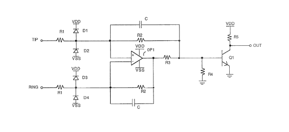
D . T TTON O TH . D AWTN t~
A better understanding of the invention may be had
from the consideration of the following detailed de-
scription taken in conjunction with the accompanying
drawing, in which FIG. 1 is a schematic diagram of the
present invention.
D .~ .R TON O TT-TF R . .R .D FMBODTM .NT
The present invention is designed to be used at
the CPE end of the telephone network, commonly called
the Tip-and-Ring. The present invention detects the
hook status of the line independent of the number of
CPEs connected to the line. When all the CPEs are on-
hook (all phones are hung-up), the present invention
will report an on-hook condition. When any CPE seizes
the line (any phone is picked up), the present inven-
tion immediately reports an off-hook condition. The
present invention also detects the presence of either A
(20 Hz) or B (16 to 68 Hz) type ringing. Because the
present invention meets F.C.C. Part 68 on-hook DC
resistance requirements (47 C.F.R. ~ 68.312(b)(1)(i)),
the circuit may be permanently connected to the Tip/
Ring conductor pair.
The circuit as shown in figure 1 is essentially a
voltage to current converter. The circuit senses the
-2-
voltage differential across the tip/ring conductors and
converts it into a proportional current, which is then
used to generate a logic level indicating the hook status
and ringing at the tip/ring. The completely floating and
balanced nature of the circuit allows for superior longi-
tudinal balance (47 C.F.R. { 68.310).
With renewed reference 'to figure , the operation of
the present invention will be described in greater
detail. As stated supra, the basin circuit is a
transconductance amplifier consisting of resistor pair
R1, resistor pair R2 and resistor R3. The input resistor
pair R1 does not need to be equal; likewise, the feedback
resistor pair R2 does not need to be equal. However, the
feedback to input resistor ratio R2/R1 must be the same
for both feedback paths. Equation 1 gives the current to
voltage transfer function, or "transconductance", gm, of
the circuit:
I R2
= gm = AuV-1 EQ. 1.
VB RlizR3
where Vp is the tip voltage minus the ring voltage
(VTIP - VRING~ see Fig. 1) and I is the output current
through resistor R3. The voltage rails are generally +5V
and -5V respectively. The feedback capacitor pair C may
be added to perfarm lowpass filtering of the output cur-
rent. With the capacitors added, the transconductance is
given by EQ. 2:
I R2 1
_ = gm = ix AixV-1 EQ . 2 .
VD RluR3 1 + sCR2
Equation 2 shows that the feedback capacitors C have
the effect of cascading a single pole lowpass filter sec-
tion, with a pole frequency of 1/CR2 rad/s, to the origi-
nal transconductance function. The filter's time con-
stant CR2 must be picked appropriately so that the fi1-
ter's 3dB point is well outside the frequency band of
interest.
-3-
To meet FCC part 68 on-hook DC resistance require-
ments, the resistors R1 must be greater than 5 beg ohms.
This high input resistance requirement makes it necessary
for the op-amp OP1 to be an FET input stage type. The
diode clamps D1 through D4 may be required to protect the
circuit from lighting and power cross conditions depend-
ing on the value of R1 and the ratio of R1/R2.
Still referring to figure , remember that VD is
defined as the tip voltage minus the ring voltage. Any
:LO positive tip/ring differential voltage will cause the
transconductance amplifier to source a proportionate cur-
rent governed by equation 2. The proportionate current
flows through resistor R4 and generates a proportionate
voltage across R4. This proportionate voltage is applied
across the base-emitter of transistor Q1, and is used to
switch Q1. Therefore, transistor Q1 is switched accord-
ing to the voltage differential present at the tip/ring
terminal. In summary, the circuit senses the voltage
differential at the tip/ring and converts it unto a pro-
portionate current, and then into a proportionate ground
referenced voltage that is used to switch a transistor OR
or OFF thereby producing a two-state logic signal. The
logic signal indicates either an on-hook or an off-hook,
or a ringing condition. The switching threshold is con-
trolled by the gm value given by equation 2 and by the
resistor R4, for a given choice of transistor.
When an on-hook condition exists, VD is approxi-
mately at battery voltage, which can be in the range of
40 to 56V. For an off-hook condition, VD will be between
4 and 18V, depending on the loop length and the 'type of
line card used at the Central Office. Therefore, a
switching threshold around 26 to 28 V is recommended.
The values of gm and R4 can be selected to guarantee that
Q1 remains in saturation for VD larger than 36V, and that
Q1 turns off for VD lower than 24V. It follows that the
circuit output is a steady logic low for on-hook
condition, and a steady logic high when an off-hook
condition is detected. If, however, the tip/ring
connection is reversed, VD becomes negative causing the
_4-
~~~~3~:~.
transconductance amplifier to go into a sink mode, and
the Q1 output is a steady logic high. Thus, the circuit
is tipjring polarity sensitive. This restriction may be
avoided by the addition of a fullwave rectifier as is
known in the art. The positive lead of the bridge must
be connected to the "TIP" lead, and the negative lead of
the bridge must be connected to the "RING" lead. The two
°'ac" leads of the bridge would then be connected to the
tip/ring leads of the line. The bridge rectifier insures
that VD remains positive regardless of the CPE tip/ring
polarity. On/off-hook detection will function, in this
case, independent of the CPE tip/ring polarity.
From the description above, it follows that when
ringing is present on the ring lead, Q1's output is a
square wave at the ringing frequency with approximately a
50~ duty cycle. If, however, the circuit is preceded by
a fullwave bridge rectifier as described supra, then
during ringing the output will be a pulse tram with a
lower duty cycle. If a 50~ duty cycle is required at the
output, the output of Q1 should be divided in half by,
for example, a flip-flop. Note: even with the bridge
rectifier, the circuit will still detect type A and B
ringing. This assumes the 3dB cut-off point of the
filter is chosen to be much higher than the ringing
frequency.
Additional items that should be noted and may not be
apparent from figure are: 1) With R1 at 5 I~eg or higher,
the circuit effectively implements a zero AC ringer
loading; 2) Completely floating and balanced circuit
implementation allows a very high level of longitudinal '
balance to be maintained at the tip/ring terminals; 3)
The Resistors R1 can be picked to any value above 5 Meg
to guarantee a DC REN of 5 or less; and 4) The circuit is
fully monolithically integrable, requiring possibly the
capacitor pair C and R1 to be external components.
In summary, the present invention represents an
improved, yet simple means of detecting on/off-hook and
ringing at the CPE end of the telephone network. The
present invention can be left permanently connected to
_5-
the line independent of the number of other CPEs on the
line. The present invention is extremely flexible,
allowing the designer to pick the circuit components.
The present invention provides a superior longitudinal
balance synthesis capability that far exceeds that of
other existing tip/ring interface circuits. Finally, the
present invention exceeds all compliance requirements.
Although the preferred embodiment of the invention
has been illustrated, and that form described, it is
readily apparent to those skilled in the art that various
modifications may be made therein without departing from
the spirit of the invention or from the scope of 'the
appended claims.
-6-