Note: Descriptions are shown in the official language in which they were submitted.
2Q~241~,
'~U 91/17485 _ 1 _ PCT/NL90/00066
1 ORGANIC PHOTOCONDUCTOR
2 FIELD OF THE INVENTION
3 The present invention relates to photoconductors
4 generally and more particularly to organic photoconductors.
BACRGROUND OF THE INVENTION
6 Various types of organic photoconductors are known.
7 Most organic photoconductors are susceptible to attack by
8 organic solvents of the type used in liquid toner
9 electrophotography and are therefore unsuitable for such
applications. These photoconductors include those which
11 dissolve in the solvents and others which are caused to
12 crack as the result of exposure thereto when they are under
13 stress, especially when under tension.
14 It is known in the art to provide protective coatings
for organic photoconductors. Examples of these coatings are
16 given in U.S. Patents 4,891,290 and 4,894,304.
17 SUMMARY OF THE INVENTION
18 The present invention seeks to provide an improved
19 organic photoconductor which is resistant to cracking in a
stressed environment wherein organic solvents of the type
21 used in liquid toner electrophotography are present.
22 There is thus provided in accordance with a preferred
23 embodiment of the present invention an organic
24 photoconductor including a base layer formed of a first
material and a photoconductive layer formed of a second
26 material, the organic photoconductor being characterized in
27 that when it is maintained in a curved orientation with the
28 photoconductive layer facing outward, the photoconductive
29 layer is subjected to less stress than the base layer. In
accordance with a preferred embodiment of the invention the
31 first material is relatively more flexible than the second
32 material. In accordance with an alternative preferred
33 embodiment of the invention the first material is relatively
34 flexible and stretchable and the second material is an
initially less flexible and stretchable material, which has
36 been chemically treated to increase its stretchability and
37 flexibility.
38 There is also provided in accordance with a preferred
WO 91/17485 2 0 8 2 4 i 6 _ 2 _ PCT/NL90/0006'
1 embodiment of the present invention an organic
2 photoconductor including a base layer formed of a first
3 material and a photoconductive layer formed of a second
4 material, the base and photoconductive layers being
pre-stressed in opposite senses.
6 There is further provided in accordance with a
7 preferred embodiment of the present invention an organic
8 photoconductor including a base layer formed of a first
9 material and a photoconductive layer formed of a second
material, the second material being chemically treated to
11 relieve stress therein. In a preferred embodiment of the
12 invention, the chemical treatment causes the photoconductive
13 layer to become more flexible and stretchable. Preferably
14 the photoconductive layer becomes more elastic or plastic.
Additionally in accordance with a preferred embodiment
16 of the present invention there is provided a method for
17 manufacturing an organic photoconductor including the steps
18 of
19 providing an organic photoconductor having a base layer
and a photoconductor layer, and
21 treating at least one of the base layer and
22 photoconductive layer to relieve stress in the
23 photoconductive layer.
24 Additionally in accordance with the above embodiment of
the invention, the base layer of the organic photoconductor
26 has greater flexibility and stretchability than the
27 photoconductor layer.
28 Further in accordance with the above embodiment of the
29 invention, the base layer has a stress relief temperature
higher than that of the photoconductive layer.
31 Additionally in accordance with the preceding
32 embodiment, the step of treating includes the steps of
33 stressing the base layer and the photoconductive layer and
34 while they are stressed, heating them to a temperature
between the stress relief temperatures of the base layer and
36 photoconductive layer.
37 In accordance with an alternative embodiment of the
38 invention, the step of treating includes the step of
2os~~~~
WO 91/17485 - 3 ~ PCT/NL90/00066
1 chemically treating the photoconductive layer to soften and
2 render it more elastic or plasi:ic that it previously was.
3 Additionally in accordancea with a preferred embodiment
4 of the invention there is provided a liquid toner
electrophotographic system including a drum, a
6 photoconductive surface providE:d on the drum, apparatus for
7 forming a latent image on t:he photoconductive surface,
8 apparatus for liquid toner de~relopment of the latent image
9 on the photoconductive surface and apparatus for
transferring the image after deavelopment thereof to a final
11 substrate, the photoconductive surface comprising an organic
12 photoconductor sheet mounted onto the drum.
13 In accordance with a preferred embodiment of the
14 invention, the photoconductor sheet is constructed and
operative in accordance with any of the embodiments
16 described above, alone or in suitable combination.
17
18
19
21
22
23
24
26
27
28
29
31
32
33
34
36
37
38
2082410
WO 91/17485 _ 4 _ PCT/NL90/00066
1 BRIEF DE8C1~IPTION OF THE DRAWINGS
2 The present invention will be understood and
3 appreciated more fully from the following detailed
4 description, taken in conjunction with the drawings in
which:
6 Fig. 1 is a simplified sectional illustration of liquid
7 toner electrophotographic apparatus constructed and
8 operative in accordance with a preferred embodiment of the
9 present invention;
Fig. 2 is a simplified illustration of an organic
11 photoconductor sheet useful in the embodiment of Fig. 1: and
12 Fig. 3 is a detailed illustration of pre-stressing of
13 the photoconductor in accordance with an embodiment of the
14 present invention.
DETAINED DESCRIPTION OF PREFERRED EMBODIMENT
16 Reference is now made to Fig. 1 which illustrates
17 liquid toner electrophotographic imaging apparatus
18 constructed and operative in accordance with a preferred
19 embodiment of the present invention. The invention is
described for liquid developer systems with negatively
21 charged toner particles, and negatively charged
22 photoconductors, i.e., systems operating in the reversal
23 mode. For other combinations of toner particle and
24 photoconductor polarity, the values and polarities of the
voltages are changed, in accordance with the principles of
26 the invention.
27 The invention can be practiced using a variety of
28 liquid developer types but is especially useful for liquid
29 developers comprising carrier liquid and pigmented
polymeric toner particles. In a preferred embodiment of the
31 invention the carrier liquid is a solvent such as Isopar
32 (Exxon). Examples of such developers are given in U. S.
33 Patent 4,794,651, the disclosure of which is included herein
34 by reference.
As in conventional electrophotographic systems, the
36 apparatus of Fig. 1 typically comprises a drum 10 arranged
37 for rotation about an axle 12 in a direction generally
38 indicated by arrow 14. An organic photoconductor 100 is
~4 91/17485 2 0 8 2 416 _ 5 _ PCT/NL90/00066
1 mounted on the drum and :.s stretched tight by stretchers 99.
2 A corona discharge device 18 is operative to generally
3 uniformly charge organic photoconductor 100 with a negative
4 charge. Continued rotation of drum 10 brings charged organic
photoconductor 100 into image receiving relationship with an
6 exposure unit including a lens 20, which focuses an image
7 onto charged organic photoconductor 100, selectively
8 discharging the photoconductor, thus producing an
9 electrostatic latent image 'thereon. The latent image
comprises image areas at a given range of potentials and
11 background areas at a different potential. The image may be
12 laser generated as in printing :from a computer or it may be
13 the image of an original as in .a copier.
14 Continued rotation of drum 10 brings charged
photoconductor 100, bearing the electrostatic latent image,
16 into a development unit 22 :including charged developer
17 plates 24. Development unit 22 :is operative to apply liquid
18 developer, comprising a solids portion including pigmented
19 toner particles and a liquid portion including carrier
liquid preferably an organic liquid, to develop the
21 electrostatic latent image. Tlae developed image includes
22 image areas having pigmented toner particles thereon and
23 background areas.
24 While development unit 22 is shown as a single color
developer of a conventional type, it may be replaced by a
26 plurality of single color developers for the production of
27 full color images as is known in the art. Alternatively,
28 full color images may be produced by changing the liquid
29 toner in the development unit when the color to be printed
is changed. Alternatively, highlight color development may
31 be employed, as is known in the art.
32 In accordance with a preferred embodiment of the
33 invention, following application of toner thereto,
34 photoconductor 100 passes a typically charged rotating
roller 26, preferably rotating in a direction indicated by
36 an arrow 28. Typically the spal:ial separation of roller 26
37 from photoconductor 100 is about 50 microns. Roller 26 thus
38 acts as a metering roller as is known in the art, reducing
CA 02082416 2000-O1-11
-6-
the amount of carrier liquid on the background areas and reducing the amount
of liquid
overlaying the image.
Preferably the potential on roller 26 is intermediate that of the latent image
areas
and of the background areas on the photoconductor. Typical approximate
voltages are:
roller 26: -200 V to -800 V, background area: -1000 V and latent image areas: -
150 V.
The liquid toner image which passes roller 26 should be relatively free of
pigmented particles except in the region of the latent image.
Downstream of roller 26 there is preferably provided a rigidizing roller 30.
Rigidizing roller 30 is preferably formed of resilient polymeric material,
such as
polyurethane which may have only its natural conductivity or which may be
filled with
carbon black to increase its conductivity.
According to one embodiment of the invention, roller 30 is urged against
photoconductor 100 as by a spring mounting (not shown). The surface of roller
30
typically moves in the same direction and with the same velocity as the
photoconductor
surface to remove liquid from the image.
Preferably, the biassed squeegee described in U.S. Patent No. 4,286,039, is
used
as the roller 30. Roller 30 is biassed to a potential of at least several
hundred and up to
several thousand Volts with respect to the potential o the developed image on
photoconductor 100, so that it repels the charged pigmented particles and
causes them
to more closely approach the image areas of photoconductor 100, thus
compacting and
rigidizing the image.
In a preferred embodiment of the invention, rigidizing roller 30 comprises an
aluminum core having a 20 mm diameter, coated with a 4 mm thick carbon-filled
polyurethane coating having a Shore A hardness of about 30-35, and avolume
resistivity
of about 10g ohm-cm. Preferably roller 30 is urged against photoconductor 100
with a
pressure of about 40-70 grams per linear cm of contact, which extends along
the length
of the drum. The core of rigidizing roller 30 is energized to between about -
1800 and
ED0~2~~.~i
WO 91/17485 - 7 ._ PCT/NL90/00066
1 -2800 volts, to provide a voli~age difference of preferably
2 between about 1600 and 2700 volts between the core and the
3 photoconductor surface in the image areas.
4 Under these conditions and for the preferred toner, the
solids percentage in the image portion is believed to be as
6 high as 35% or more. It is prei'erable to have an image with
7 at least 25-30% solids, after rigidizing.
8 Downstream of rigidizing roller 30 there is provided
9 apparatus for direct transfer- of the image from organic
photoconductor 100 to a substrate 130 such as paper. The
11 direct transfer is effected by the provision of guide
12 rollers 132, 134 and 136, which guide a continuous web of
13 substrate 130, and a drive roller 138, which cooperates with
14 a support web 140. A suitab7.e charging device, such as
corona discharge device 142, charges the substrate at a
16 transfer location, for effecting electrophoretic transfer of
17 the image from photoconductor 100 to substrate 130.
18 Following transfer of the toner image to substrate 130,
19 photoconductor 100 is engaged by a cleaning roller 50, which
typically rotates in a direction indicated by an arrow 52,
21 such that its surface moves in a direction opposite to the
22 movement of adjacent surface of: photoconductor 100 which it
23 operatively engages. Cleaning roller 50 is operative to
24 scrub and clean photoconductor 100. A cleaning material,
such as toner or another cleaning solvent, may be supplied
26 to the cleaning roller 50, via a conduit 54. A wiper blade
27 56 completes the cleaning of the photoconductor surface. Any
28 residual charge left on photoconductor 100 is removed by
29 flooding the photoconductor surface with light from a lamp
58.
31 In a multi-color system, subsequent to completion of
32 the cycle for one color the cycle is sequentially repeated
33 for other colors which are sequentially transferred from
34 photoconductor 100 to substrate: 130.
Alternatively the direct. transfer apparatus may be
36 replaced by an intermediate transfer member which receives
37 the images from photoconductor 100 and transfers them to the
38 final substrate.
~0~~~~
WO 91/17485 - 8 - PCT/NL90/00066
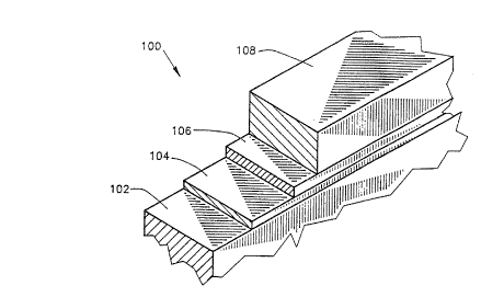
1 Fig. 2 illustrates a preferred organic photoconductor
2 sheet 100, useful in the embodiment of Fig. 1. The sheet
3 comprises a base layer 102, typically formed of Aluminized
4 Polyethylene Telephthalate, which is commercially available
under the trademark Mylar. The base layer is preferably
6 about 80 microns in thickness and has a melting point of
7 250" C.
8 Disposed above the base layer 102 is a sublayer 104,
9 typically formed of Polyester, Toluenesulfonamide
formaldehyde resin and Polyamide and having a thickness of
11 about 0.2 microns. Disposed above the sublayer 104 is a
12 charge generation layer 106, typically formed of
13 Hydroxysquarylium Dye and Toluenesulfonamide-resin and
14 having a thickness of about 0.3 microns.
Disposed above layer 106 is a charge transport layer
16 108, typically formed of Polyester, Polycarbonate, Yellow
17 Dye, 4-[N,N-diethylamino] benzaldehydedipenylhydrazone and
18 Polysiloxane in a minor proportion, having a thickness of
19 about 18 microns. Charge transport layer 108 and charge
generation layer 106 together define the photoconductive
21 layer referred to above.
22 The organic photoconductor described so far is
23 commercially available from IBM Corporation under the trade
24 name Emerald.
In accordance with an embodiment of the present
26 invention, and as illustrated in Fig. 3, the organic
27 photoconductor, as received from IBM Corporation, is
28 subjected to an annealing procedure which will now be
29 described in detail.
According to one embodiment of the invention, organic
31 photoconductor 100 is mounted on a stretcher 120 and
32 tensioned to a strain of 3 Kg per cm of width of
33 photoconductor 100. While subject to the above strain,
34 photoconductor 100 is heated, preferably in an oven (not
shown) to a temperature of 60° C, for about 30 minutes.
36 Thereafter, photoconductor 100 is cooled to room temperature
37 and thereafter, the external stress is removed therefrom.
38 It is noted that the temperature of 60 degrees lies
20~~~~.
WO 91/17485 _ 9 ,_ PCT/NL90/00t166
1 intermediate the stres;~ relief temperature of base layer
2 102, which is approximately 150° C and the glass transition
3 temperature of charge transport layer 108, which is
4 approximately 45° C.
After treatment in the m<inner described above, i.e.,
6 after the external stres:a is removed from sheet
7 photoconductor 100, charge transport layer 108 of
8 photoconductor 100 remains stressed under compression, while
9 base layer 102 remains stressed under tension. When
photoconductor 100 is mounted on drum 10 as illustrated in
il Fig. l, and subject to external tension, charge transport
12 layer 108 is either in compression or becomes relatively
13 free of stress, and therefore is less susceptible to
14 cracking or other defect geaneration as the result of
exposure to organic solvents,, such as Isopar, which are
16 common in a liquid toner electrophotographic environment.
17 For example, an organic photoconductor 100 which was
18 not annealed as described above, developed cracks after
19 about 500 copy cycles in a liquid toner copier. In contrast,
an organic photoconductor which was treated as described
21 above developed no cracks, even after several tens of
22 thousands of copy cycles. It should be noted that annealing
23 the sheet photoconductor without subjecting it to
24 simultaneous tension does noi: substantially improve the
Isopar resistance of the photoconductor.
26 In accordance with an a:Lternative embodiment of the
27 present invention, organic phoi~oconductor 100 may be treated
28 chemically to reduce stress cracking in a liquid toner
29 environment. In accordance with this embodiment, the charge
transport layer is treated wii~h a solvent or other reagent
31 to soften charge transport layer 108 and to render it more
32 stretchable, i.e., more pla:~tic or elastic than it was
33 previously.
34 The chemical treatment is selected so as to leave the
electrical and optical characteristics of the photoconductor
36 essentially unchanged. When such a chemically treated
37 photoconductor sheet is stretched around drum 10, stress
38 does not develop in charge transport layer 108. Accordingly,
~a~~"~-_ ~.
w ~~ .~ i)
WO 91/17485 _ 10 _ PCT/NL90/00066
1 when stretched photoconductoi- 100 is exposed to organic
2 solvents it does not tend to crack.
3 A specific chemical treatment which has been found to
4 be effective is dipping of photoconductor 10o in
cyclohexanone diluted by isopropyl alcohol in the ratio 1:5
6 for 2 minutes. This treatment does not significantly change
7 the electrical and optica7L characteristics of the
8 photoconductor but eliminates cracking as described above.
9 An alternative chemical t~.~eatment employs cyclohexanone
alone or vinyl modified epoxy 1A24, commercially available
11 from HumiSeal Division of Co:Lumbia Chase Corporation of
12 Woodside, NY, diluted 1:20 with cyclohexanone. These
13 materials can be applied by a wire-rod technique on the top
14 surface of photoconductor 100. In such a case, an RK Print-
Coat Instrument Ltd. of Litl:ington, Royston, Merts., UK,
16 Model KCC 303 coater, using bar #2 (rod diameter 13 mm, wire
17 diameter 0.15 mm) may be operated with bar linear speed of
18 70 mm/sec.
19 If pure cyclohexanone i:a used, then the results are
similar to those for dipping, and the solvent evaporates
21 within about 20-30 seconds.
22 If the mixture of cyclohexanone and epoxy is used,
23 then in addition to the above described effects of the
24 cyclohexanone, the residual vinyl modified epoxy forms a
mechanically protective overcoating which is substantially
26 abhesive to toner particles rafter the evaporation of the
27 solvent.
28 It will be appreciated b:y persons skilled in the art
29 that the present invention is not limited by what has been
particularly shown and described hereinabove. Rather the
31 scope of the present invention is defined only by the claims
32 which follow:
33
34
36
37
38