Note: Descriptions are shown in the official language in which they were submitted.
WO 91/19219 PCI/GB91/00822
-- 1 --
2082939
FABRY-PEP~OT MODULATO~
This invention relates to Fabry-Perot modulators and
in particular, but not exclusively, to those employing a
multiple quantum well active region.
Since the first observation of the effect of
electric fields on the optical properties of GaAs-AlGaAs
quan~um well (QW) structures a number of optoelectronic
devices have been demons~rated which exploit the enhanced
electro-absorptive properties of QW structures, e.g. fast
intensity modulstors and hybrid optical logic elements,
both bistable and non-bistable. These devices employ a
QW layer or multiple quantum well (MQW) grown epitaxially
as the intrinsic region of a pin diode that can operate
as an electro-absorptive modulator and efficient
photodetector simultaneously.
A contrast ratio (on:off) of -2:1 has been observed
in transmission devices with only - 1 ~m of MQW absorber
usually consisting of wells and barriers each about 100-
thick. This is very efficient, given the device size,
but a better contrast ratio is desirable. By 'contrast
ratio' is meant the ratio of the high : low output
states, irrespective of whether the device switches on or
off with applied bias. 'Modulation depth' is the
absolute change in state, which in reflection or
transmission terms can only be between 0 and 1.
It might at first seem that in order to obtain
better contrast or modulation figures one would simply
increase the ~hickness of the MQW layer. However, the
situa~ion is complicated by a variation of the elec~ric
field across the intrinsic region of the PIN device which
results from the relatively high background doping level
WO 91/19219 PCI~/GB9t/00822
-- 2
2082939
of this layer. The background doping level has had a
lower limit of ~ lxl015/cm3 in the best available material
(this is not a fundamental limit and depends on the
material and growth conditions), and is routinely two or
three times this value. The resultant significant
variation in the electric field causes a broadening of
the absorption edge of the MQW material even at zero bias
and, moreover, produces a different red shift of the
excitonic absorption in each well as an external bias is
applied to the device for modulation. As the bias is
increased the sbsorption edge broadening becomes worse
due to the roughly parabolic dependence of the edge shift
on applied field. So, instead of producing a larger
change in the intensity of a transmitted or reflected
beam of light the increase in thickness of the absorbing
layer might only serve to distribute absorption changes
over a wider spectral region and leave the modulation at
the operating wavelength relatively unaffected.
Optimisation calculations have shown that if the
residual doping is 2xlO~5/cm3 it is best to use about 45
wells of 100A GaAs separated by barriers of 100A
A10 3GBO 7AS confirming the limit of around l ~m for the
~otal thickness.
A second disadvantage of increasing the MQW
thickness is that an increased voltage is required to
induce a given change in absorption. It has been
proposed that QW devices be integrated in 2-dimensional
arrays with Si-based LSI electronics to form-
high-bandwidth optical interconnects, and in this case
drive volta~es for such modulators or logic gates will be
limited to a few volts.
One method of improving modulation in a device that
has limitations on its absorber thickness and drive
voltage is to increase the effective optical path length
by incorporating the MQW pin diode into a Fabry-Perot
etalon.
WO 91/19219 PCI/GB91/00822
-- 3
2 082939 -~
Asymmetric Fabry-Perot modulators (AFPMs) containing
quantum wells have recently been demonstrated, which
exhibit contrasts of - 13-20dB in reflection with low
insertion loss and 9-lOV bias (2,3). In this case the
front and back cavity mirrors are formed by the
air/semiconductor interface (R - 0.3) and an integrated
semiconductor multiple quarter-wave stack (R > 0.95)
respectively. The enhanced modulation is achieved by
using the attenuating effect of MQW electro-absorption at
a resonant wavelength of the Fabry-Perot cavity in order
to match front and effective back mirror reflectivities,
at which point the net cavity reflection must fall to
zero. Devices of this type can be readily made in planar
arrays with low coupling losses, and are therefore of
considerable interest as interface elemen~s for optical
interconnects.
Compatibility of the modulator voltage swing with
that directly attainable in high-speed electronic
circuits (5V or less) is clearly desirable. To achieve
these lower drive voltages, a number of options are
available. Firstly, the number of wells can be reduced.
Recent calculations have indicated than an AFPM
containing 31 x (lOOA GaAs well + 60A Alo3GaO 7As
barrier) should achieve a peak contrast of - lOdB at only
~ 3.3V bias (4).
Secondly, if the cavity finesse is increased by
integrating a front mirror of higher reflectivity than
the usual - 0.30, the critical amount of absorption
required for the zero off state is reduced (5). This
option has recently been demonstrated by Yan et al. (6),
who achieved over 7dB contrast with only 2V bias. A
disadvantage is that the increase in finesse leads to
reduced optical bandwidth and higher insertion losses for
WO 91/19219 PCr/GB91/00822
2082939
a given background absorption, along with increased
sensitivity to temperature and cavity thickness
fluctuations.
We hsve realised that there is a third spprosch by
means of which operating voltage requirements can be
reduced or the contrast ratio for a given operating
voltage increased.
According to a first aspect the present invention
provides a Fabry-Perot modulator comprising a resonant
cavity defined by front an~ back reflective surfaces of
different reflectivities and including within the cavity
a multiple quan~um well structure in which the barrier
width is sufficient to prevent resonant coupling between
the wells in the structure, wherein the absorption of the
quantum well structure at a resonant wavelength of the
cavity and at a low bias level is greater than with a
higher bias level, whereby the reflectivity of the
Fabry-Perot modulator at that wavelength increases with
an incresse in bias level.
With such an arrangement it is possible to have a
very low (nesr-zero) cavity reflectivity at low bias and
obtain significant reflectivities with relatively modest
bias levels. And because the 'off' state is so low, very
large contrast ratios (~100:1) are achievable.
Alternatively, one can obtain normal (say 3:1 to 5:1)
contrast ratios with lower than usual bias levels.
Preferably substantially all of the barrier layers
in the MQW structure are at least 40A thick.
Preferably the MQW comprises a plurality of wells
having a width of between 130 and 160A. More preferably
the well width is a~ least 140A. Most preferably the
well width is at least 145A.
Preferably the MQW comprises barrier layers having
widths of between 40 and lOOA. More preferably the
WO 91/19219 PCr/GB91/00822
-- 5
2082939
bsrrier width is no more than 70A. Most preferably the
barrier width is between 45 and 65A.
Preferably the MQW structure comprises no more than
30 wells.~ More preferably the MQW has between 10 and 30
wells.
In the letter by K.K. Law et al, published in Appl.
Phys. Lett. 56(19), 7 May 1990, 1886 - 1888, there is
described a normally-off AFPM which utilises the Wannier-
Stark localization in a superlattice (SL). (A
superlattice structure is distinct from an MQW structure
because the barriers in a superlattice are thin enough
for there to be substantial resonant coupling between
adjacent wells. In an MQW structure the barriers should
be of a thickness sufficient to ensure that the wells
remain quantum mechanically isolated. Law et al used a
superlattice consisting of 100 half pairs of 30A GaAs/30A
Alo 7 GaO 3 As.) When an electric field is applied along
the growth direction of an SL, the resonant coupling
between the QWs of the SL is destroyed because the energy
levels in adjacent QWs become misaligned and the
eigenfunctions localize over a few adjacent QWs. This is
called Wannier-Stark localization and gives rise to a
change of absorption edge from that of a miniband profile
to a sharp QW excitonic shape. Associated with the wave
function localization, there is an effective blue shift
of the absorption edge because the SL band gap is smaller
than that of the isolated QW level. Conventional QWs of
course give a red shift when a field is applied. Law et
al report that, at higher applied fields, the initially
observed blue shift becomes a red shift (with an applied
voltage of 6 volts or more) as the result of competition
between the blue shift due to Wannier-Stark localization
and the red shift corresponding to the combination of the
quantum confined Stark effect due to the field-induced
WO 91/19219 PCr/GB91/00822
2082939
deformation of the QW potential and of the enhancement of
the exciton binding energy caused by the localization.
Law et al report that for a voltage swing of 8 volts, the
reflectivity at the zero-bias FP resonance wavelength was
seen to increase from -0.4% to -25%, equivalent to a
contrast ratio of 62.5:1. Law et al also mention that
the contrast ratio varies rapidly as a function of
wavelength, but that with an applied bias of 8 volts a
contrast ratio greater than 10 can be attained over an
optical bandwidth of 25A, somewhat smaller than that of a
normally-on device reported by Yan et al (Photon. Tech.
Lett. 2, 118,1990). It is not clear how the performance
of devices of the type described by Law could be
improved.
The present invention provides a device structure
which would appear to offer performance better than that
of comparable devices of the type described by Law. In
particular, devices according to the invention
potentially offer lower bias and lower insertion losses
for a given contrast ratio.
Preferred embodiments of the invention will now be
described, by way of example only, with reference to the
accompanying drawings in which:
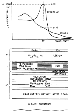
Figure 1 shows schematically for a 'wide' QW
structure the absorption against wavelength in the
biased and unbiased states;
Figure 2 shows schematically the corresponding
behaviour of a 'conventional' QW structure;
Figure 3 shows a schematic vertical section through
a device according to the invention;
Figure 4 shows reflection, reflection contrast and
reflection changes for a device according to the
invention; and
WO 91/19219 2 0 8 2 9 3 9 PCI`/GB91/00822
-- 7
Figure 5 shows schematically a SEED according to the
present invention.
In our co-pending PCT patent application
(GB90/00282) we describe and claim an asymmetric
Fabry-Perot QW modulator (AFPQWM) in which the QW
structure has in the unbiased state a low absorption at a
resonant frequency of the EP cavity. By applying a bias
to such a device, absorptiGn in the QW is increased and
hence the reflectivity of the modulator is reduced. In
Figure 2 absorption is plotted against wavelength for
such a QW structure (which will typically have a well
width of lOOA) for two bias levels. The optimum
wavelength of operation of such a structure in an AFPQWM
of the type described in GB90/00282 is shown at point BA
(Bias Absorbing). Such a QW structure is combined with a
Fabry-Perot cavity, the properties of the QW structure
and the resonance frequency of the cavity being chosen
such that a Fabry-Perot resonance coincides with a low
initial absorbing state in the unbiased QW at a
wavelength at which a relatively highly absorbing state
is available in a biased condition.
In Figure 1 there is shown an equivalent plot for a
QW structure, which, if made from the same materials as
the device whose behaviour is illustrated in Figure 2,
has a greater well width. Typically, if the wells of
both devices were made of GaAs and the barriers of
Alo 3GaO 7As, the well width for Figure 1 behaviour would
be 145-150A, while for Figure 2 the width would be lOOA.
In Figure 1 the wavelength corresponding to the peak of
the absorption in the unbiased state is marked BT, to
signify the optimum bias transmitting point.
The differences between the absorption profiles
represented in Figures 1 and 2 are significant. In
devices according to the invention we take advantage of
WO 91/19219 PCI/GB91/00822
-- 8
2082939
the fsct that in QW structures having absorption profiles
such as that shown in Figure l, which we will here refer
to as the 'wide-well' case, most of the absorption change
between the biased and unbiased situation occurs at the
absorption peak shown, and rather poor changes at the
wings of the profile. Put another way, with structures
of this type, the biggest absorption change occurs at the
wavelength at which, in the unbiased state, absorption is
strongest. Furthermore, the wide-well structures are
more sensitive to electric fields than the narrow well
samples (ref. Whitehead et al, Appl. Phys. Lett. (1988),
53, 956-8).
With this in mind, we choose QW structures which
have a high initial (ie unbiased) absorption, and then
arrange to bias the device to reduce its absorption and
hence increase the reflectivity of the Fabry-Perot
modulator. In practice, some absorption remains in the
biased state, and this residual absorption limits the
amount of reflectivity that one can obtain from a
Fabry-Perot modulator of this type. Our calculations
indicate that it is possible to achieve, at room
temperature, reflectivities of up to 25 to 30 percent and
yet still provide a near-7.ero reflectivity in the
unbiased state.
For QW structures of the type whose absorption
spectrum is illustrated in Figure 2, typically
GaAs/GaAlAs structures with wells 80 to llOA wide, there
is a well defined absorption peak both in the unbiased
and the biased state. The peak remains well resolved in
~0 the shifted form and it is possible to obtain a strong
modulation effect by operating close to the absorption
edge tas described in GB90~00282 for a normally-on
device). However, for a normally-off device, ie one
where there is low reflectivity/high absorption in the
WO 91/19219 2 0 8 2 9 3 3 PCT/GBgl/00822
q
unbiased state, the level of absorption in the 'on-state'
is too high. Note the relative scales of Figures 1 and
2. The absorption peak in Figure 1 is about 1300 cm l,
while in Figure 2 it is roughly twice as high.
The peak in the unbiased absorption spectrum in
Figure 1 corresponds to the el-hhl exciton peak. It is
this exciton peak that we arrange to coincide, under low
electric field conditions, with a resonance of the
asymmetric FP cavity, to give low cavity reflection - the
"off" state. On applying an electric field, the exciton
shifts and loses oscillator strength rapidly, and the
cavity reflection increases as the absorption falls.
With 150A wells of GaAs with 60A AlGaAs barriers, the
critical absorption for effectively zero reflectivity is
achieved with about 30 wells, in which case the
theoretical contrast is more than 30dB with about 6dB
insertion loss. These figures are obtained for a voltage
swing of just over 5 volts.
In Figure 3 there is shown a Fabry-Perot modulator 2
comprising a resonant cavity 4 defined by a front
reflective surface 6, of reflectivity R~, which may be
formed by the natural semiconductor surface or by a
reflective coating thereon, and a back reflective surface
8, of reflectivity R~. The cavity is formed of the
front, AlGaAs, region 10, which in this example is n+,
and the intrinsic, quantum well region 12 which comprises
150A GaAs well regions separated by 60A Alo 3Ga0 7As
barriers. The total thickness of regions 10 and 12 is
intended, in this example, to be such that resonance
occurs at 862nm - which is the wavelength of the el-hhl
exciton for 150A quantum wells at low field. An optional
50A capping layer of GaAs which overlies the AlGaAs
region 10 is intended for contacting purposes and is thin
WO 91/19219 PCr/GB91/00822
-- 10 --
2082939
enough to have a negligible absorptive effect on the
light passing through it.
The multilayer stack reflector 14, which serves as
the back reflector of the cavity, is a 15 period stack
which comprises alternating layers of Alo IGaO gAs and
AlAs. The ternary layers of the stack 14 are 609A thick,
the binary layers 723A. The uppermost layer of the
stack 15, which is the one in contact with the MQW
region 12, is formed of the high index material. This
copmost layer of the reflector stack 15 is preferably
left undoped in order to guard against possible upward
dopant diffusion into the MQW structure.
The multilayer reflector stack, and others like it,
have been shown (2) to give reflectivities of 0.95 or
more. Different reflector stacks can be used,
reflectivity depending upon the refractive index
difference between the component layers of the stack and
upon the number of layers: in general fewer periods will
lower the reflectivity, while more will tend to increase
it.
The absorption coefficient of the MQW device can be
altered by the application of a bias vol~age in a known
manner. The resonant MQW etalon modulator of Figure 1
was modelled in a simple way, with more emphasis on the
electric field-induced absorption and refractive index
changes (although the index changes, which are generally
negligible even for standard lOOA AFPM devices, are even
smaller for the wide-well devices) in the MQW layer and
the manner in which they combine with the properties of
the basic resonant cavity, rather than considering in
detail the subtleties of the multiple layers which may
make up the cavity. For example, we have avoided
multiple matrix-type calculations required to simulate
WO 91/19219 2 0 8 2 9 3 9 PCT/GB91/00822
the spectral reflectivity properties of dielectric stack
mirrors. The main approximations made are
(a) Spectral dispersion and spatial variation of
the zero-bias cavity refractive index are ignored.
By 'spatial variation' we refer to the index of the
different layers of GaAs and AlGaAs that may make up
the cavity. A weighted mean index n~ of 3.37 was
calculated for the cavity at 850 nm, based on the
effective AlGaAs content of a typical MQW pin
structure and published experimental index data for
this material and this was kept constant throughout.
The justification for this is that in the small
wavelength band which would be considered for device
operation the spectral variation of the refractive
index is so small that it has no significant effect
on the modulation characteristics. Furthermore, as
long as the calculated mean index lies somewhere
between that of GaAs and AlGaAs at the operating
wavelength, there is no effect on the magnitude of
the modulation achievable with a cavity of given
finesse. The effect of the change in index induced
by an applied electric field is a much more
important consideration.
(b) The cavity mirrors are assumed to be 'hard'
reflectors, i.e. we ignore the finite thickness of
the mirrors which would be used in a practical
device, and assume all reflections to occur at the
interfaces between the cavity material and the
mirrors. These would probably consist of multiple
quarter-wavelengths of dielectrics of different
refractive indices (when high finesse is required),
plasma-deposited (in the case of dielectrics) and
could either be evaporated or epitaxially
2082933
WO 91/19219 PCI/GB91/00822
-- 12 --
integrated, perhaps as the p and n regions of the
pin structure. The specific details of how the
front and back surface reflectivities are achieved
are not critical to the calculations of the optimum
device modulation properties.
(c) We have not included the linear electro-optic
(LEO) effect, which we would expect to become
comparable to the electro-refractive effect only at
longer wavelengths, outside the region considered
here. The polarisation dependence of the LEO
contribution to modulation has recently been
observed in a high-finesse device.
The cavity length of the Figure 3 arrangement is L, and
is set at a value around 1.7~m, which places the F-P
resonance in the wavelength region of interest and is
also in keeping with typical epitaxial structure
thicknesses. The cavity length includes the thickness of
all MQW layers and the thickness of the n+A13Ga7As layer.
The use of a cavity length of an odd integral number of
quarter wavelenghts is necessary because it places the
F-P resonance at the desired wavelength. When the figure
3 structure is modelled using full multi-layer matrix
calculation methods we find that in the case of the high
finesse device (which would have another multilayer stack
on top instead of the simple AlGaAs layer) the cavity
thickness (length) L is defined only by-the MQW thickness
i.e. the MQW/MLS boundary defines the mirror reflection
point. In this case the cavity thickness, L, must indeed
be an integer number of 1/2 wavelengths (the operating
wavelength). However, when modelling the asymmetric
structure, the cavity is more probably defined by the
total thickness of the M~W + AlGaAs top layer, and in
this case, to put the F.P. resonance at the required
W O 91/19219 2 0 8 2 9 3 9 PC~r/G B91/00822
wavelength, L must be an odd integral number of quarter
wavelengths. (Whether one makes the "cavity" mA -1/2
with m even, or mA/4 with m odd, depends on whether the
top layers of the MLS is low index or high index
respectively. The mirror will be highly reflecting for
both cases.) Because of the asymmetry the cavity is
subtly different from the high-finesse case, but the
observation above has been confirmed by other workers
with access to multi-layer simulation programs. For a
cavity such as the one in Figure 3, with a mean
refractive index nm and linear absorption a (in the MQW
region only), in the planewave approximation at normal
incidence, the transmission T and reflection R are given
by the following equations:
T = AR = (B + F sin2~) where
(1 + F sin2~)(1 + F sin2~)
F = 4RaA = e C~ R~)(l-Rb)
(1 - RC)2(1 - RC)2
B = Rf (1 - RC/Rt)'/(l-Rc)2
and
Ra = (RtRb)e 5d ~ = 2~ nmL/A
Cavity finesse = (~/2) F1/2
where Rf is the reflectivity of the front surface,
Rb the reflectivity of the back reflector, d is the
thickness of the MQW layer, ~ the absorption at
wavelength A, L the cavity length and nm the average
refractive index.
The data used for modelling were derived from rocm
temperature transmission spectra, which are in reference
WO 91/19219 PCI/GB91/00822
- 14 2 08 29 39
7, over the range 800-920 nm. By performing a
Kramers-Kronig integral on this data we have obtained the
corresponding spectra for electro-refraction. Because of
the minimal changes in absorption outside the wavelength
range 810-900 nm, we set these as the limits for the
Kramers-Kronig integral. These spectra actually take
into account possible contributions from the
field-induced 'forbidden' transitions which occur above
the MQW absorption edge at energies below the n = 2
sub-band edge and which begin to dominate the absorption
spectra at high applied fields.
If we choose the cavity length so that a reflection
resonance occurs at or about a peak, such as the el-hhl
exciton peak, of the unbiased MQW absorption spectrum,
where a is initially high, then the resonant reflection
must remain low. The condition to achieve precisely zero
reflectivity is:
ad = 0.5 ln (Rb/R~) (l)
which, for our chosen reflectivities, means that ad
~ 0.58. The electro-absorptive properties of the MQW can
then be used to tune the cavity so that R becomes as
large as possible. We estimate that the absorption
coefficient at the exciton peak can be reduced from about
13000cm l to a minimum of about 4000cm 1 by applying a
field of about 86kV/cm (which gives a total field of ~
lO0 kV/cm, since there is always a built in field of -
1.3V) for the wide-well sample. The optimum operating
wavelength is selected automatically in our calculation
scheme to give the maximum contrast for a given upper
limit on the insertion loss. Having found the optimum
wavelength, the cavity length is ser so as to put the
cavity resonance at the wavelength.
In Figure 6 there is shown the calculated maximum
WO 91/19219 2 0 8 2 9 3 9 PCI /GB91/00822
- 15 -
contrast and insertion loss (at resonance) as a function
of the number of 150A wells in an AFPM. The critical
absorption for zero reflectivity is achieved with about
30 wells, in which case the theoretical contrast is more
than 30dB with only about 6dB insertion loss. These
figures are for a voltage swing of just over 5 volts,
calculated by assuming that the average field of about
86kV/cm exists only across the MQW region, which in this
example has 60A barriers of Alo3GaO7As. If one is
interested in operation at even lower voltages, one can
use fewer wells and still obtain reasonable contrast.
For example, a structure containing only 15 of the above
wells should provide a peak contrast of about 7dB, with
only about 3dB insertion loss, and with a voltage swing
of only 2.6 volts. Even fewer wells may be used where
this is appropriate, or an intermediate number of wells
may be used to obtain properties intermediate those set
out above.
A structure containing 15 wells as described above
was grown using a conventional MOVPE growth technique.
Prior to device fabrication the wafer was scanned at
normal incidence, using an optical multi-channel
analyser, in order to determine the areas with the most
suitable reflection characteristics (correct cavity
thickness). Simple mesa diodes (~ 500~m x 500~m) with
windowed top contacts were fabricated from selected
regions using standard photolithography, metallization
and wet chemical etching. Devices were mounted and
wire-bonded onto TO5 headers for biased reflectivity
measurements. All reflection spect.a were measured at
normal incidence and room temperature using a
computer-controlled scanning monochromator system, with
lock-in detection for the reflected signal. These
spectra were then normalized to that from a
~5 freshly-deposited Au film.
WO 91/19219 PCI`/GB91/00822
- 16 - 2 0 8 29 39
Figure 4 shows the behaviour of the 150A-well AFPM
with various applied voltages. The operation is as
expected - the resonant reflectivity increases with
incressing field, and with a fairly broad bandwidth. We
find that to achieve the lowest off-state the device must
be forward biased so as to offset the built-in field,
estimated to be 50kV/cm for such a thin MQW region, and
restore the absorption at the exciton peak. There is
excellent agreement between theory and experiment for the
maximum contrast, which we find to be ~ 6.7dB (4.7:1) for
a voltage swing of 3.5V. This voltage is a little higher
than expected, but is almost totally due to the undoped
Alc IGaO gAs layer in the i-region. Peak insertion loss
is only 3.2dB. The optical bandwidth for 3dB contrast
is ~ 6nm, which is also the bandwidth over which %R is at
least 0.3. It is also worth noting that the device is
capable of > 3dB contrast with a swing of only lV(+lV to
OV), albeit with a higher insertion loss (~ 6dB). An
interesting feature of the normally-off AFPM operation is
its compatibility with the characteristics required for a
self-electro-optic effect device (SEED) (9). The
absorption and photocurrent both fall with increasing
applied field at resonance, and the active (MQW) region
is thin enough that photodetection efficiency remains
very high even into forward bias.
The AFPM structure incorporating wide wells and
operating in a normally-off mode can be used for very low
voltage modulation. Devices such as these may be
important for high speed optical interconnection of
electronic circuits and for high contrast SEED elements
and arrays.
There are two conflicting considerations for the
barrier layer thickness. First, the barrier layers need
to be sufficiently thick for the wells to remain quantum
WO 91/19219 2 0 8 2 9 3 9 PCI`/GB91/00822
-- 17 --
mechanically isolated. I~ the barrier layers are thinner
than this, the structure will lose the essential nature
of a quantum well and will instead act merely as a
superlattice (which do not have such good
~ electro-absorption characteristics). On the other hand,
one wants to minimise the barrier layer thickness in
order to minimise the necessary bias voltage of the
device. The barrier layers themselves make no useful
contribution to the device's optical absorption.
Preferably, therefore, the maximum barrier thickness is
no more than 100A. In view of the desire to use a low
operating voltage, barrier thicknesses are preferably
less than 100A, for example less than 90A, more
preferably less than 80A, yet more preferably less than
70A. Others have reported, in other contexts, the
successful use of barrier layers as thin as 40A, and we
see no reason why such barrier layers should not be used
in structures and devices according to the invention.
Thus barriers having thicknesses in the range 40A to 100A
are of interest, preferably in the range 40A to 80A, more
preferably 40A to 70A and most preferably 45A to 65A.
Typically we use barrier thicknesses in the range 50A to
60A.
In combination with barriers having widths in the
ranges set out in the preceding paragraph, we have used
wells having widths of about 150A.
The choice of well width determines the change in
absorption which is achievable at the operating
wavelength for a particular swing in bias voltage. For
devices according to the invention, one needs a structure
in which the level of absorption in the biased state is
low enough to give a satisfactory reflectivity in that
biased state while also having a high enough absorption
in the unbiased state to give a very low reflectivity.
20829~g
WO 91/19219 PCI/GB91/00822
- 18 -
Thus it is not enough merely to find a large or
relatively large /.a. After extensive study of the
absorption characteristics of quantum well structures, we
favour the use of well widths in the range 145A to 150A
because they have particularly suitable absorption
characterlstics. Well widths outside this range, for
example 140A to 155A, may be used but will not normally
offer such a good combination of characteristics. Well
widths outside this latter range are not recommended,
since they are predicted to have still less desirable
characteristics. Well widths much above 150A, for
example above 160A, will result in an almost bulk GaAs
property, with the consequent inferior electroabsorption
properties. Conversely, use of well widths below 130A
will give higher absolute absorption figures but with the
disadvantage of undesirably high absorption in the biased
state.
The two preceding paragraphs should be read in
conjunction. In particular, the ranges and preferred
ranges for the well and barrier widths should be
considered together - the most preferred structures being
those with barrier widths in the range 50A to 60A with
well widths in the range 145A to 150A. Preferred
structures include any combination of barrier and well
widths from any of the preferred ranges.
The barrier and well thicknesses and combinations
set out in the preceding paragraphs are appropriate for
QW structures comprising GaAs wells and AlxGalxAs
barriers, the barriers typically having an aluminium mole
fraction near x = 0.3. However, the invention is in
principle applicable to other materials systems -
provided that QW structures made from such materials
systems have suitable absorption spectra. A 'suitable'
absorption spectrum will normally contain an excitonic
WO 91/19219 2 0 8 ~ 9 3 9 PCl/GB91/00822
- 19 -
peak in the unbiased or low biased state, which peak is
made coinciden~ with a resonance of the FP cavity, and
which peak can be "biased-out" to a desired change in
absorption.
Structures according to the invention also find
application in self electro-optic devices (SEED).
Conventional SEED structures use optically non resonant
structures - see for example the chapter (Chapter 14) by
Chemla and Miller in "Heterojunction Band Discontinuities
- physics and device applications", published by.
North-Holland, 1987, and the references thereto. In
general the SEED is an optical switch which consists of a
QW modulator connected in series (electrically) with
another electronic or optoelectronic device. An I(V)
relationship will relate the current through and voltage
across the series device. Because the p-i-n QW structure
of the SEED also acts as a closely coupled
detector/modulator, the current and voltage are also
related by the response function of the SEED - which
depends upon A and Pin, where Pin and A are the power and
wavelength of the light incident on the device,
respectively. These two relations have to be satisfied
simultaneously and this gives rise to the possibility of
electronic feedback on the optical behaviour. The
feedback can be positive or negative, depending upon the
operating wavelength. Both types of feedback have been
exploited in optically bistable devices, self-linearized
modulators and optical level shifters. While such
devices have been demonstrated both in the propagation
mode normal to the QW and in a waveguide orientation, the
applicability of structures according to the present
invention as SEEDs appears to be limited to devices in
which the propagation mode is normal to the layers of the
QW.
WO 91/19219 :2 0 8 2 ~ 3 9 PCI`/GB91/00822
- 20 -
AFPMs according to the invention, that is those
whose reflectivity is very low in the unbiased state due
to the coincidence or near coincidence of a peak in the
unbiased absorption with a resonance of the FP cavity,
can simply replace the QW structures of known SEED
structures. The benefit of replacing the non-resonant
reflection mode QW structures of known SEEDs with those
according to the present invention is that it provides a
means of improving the contrast ratio of the SEED.
Typically, prior art SEED switches have on/off ratios of
about 3:1.
It is worth noting, in this context, that although
SEEDs according ~o the present invention are resonant
structures, their linewidth is no narrower ehan the
excitonic feature that one is using. In fact, in
general, the device's linewidth is slightly wider than
the excitonic feature.
As with other SEED structures, SEEDs according to
the invention are temperature sensitive. Because
satisfactory operation of the device depends upon the
relationship between the FP resonance and the absorption
feature, features which move with temperature, but at
different rates, SEEDs and the other devices according to
the invention will need a controlled-temperature
operating environment. The absorption edge shifts by
about lnm for every 3 Kelvin. Normally, an operating
range of 1 10C will be possible. Such a range is
comparable to that required by "ordinary" QW modulators.
Typically one or more Peltier coolers will be used to
control device temperature.
In the embodiments described above, the Fabry-Perot
cavity has been defined by various surfaces of the
semiconductor structure, this is not an essential
feature of the devices. The quantum well structure and
WO 91/19219 21 2082939 PCT/GB91/00822
one or both of the reflectors defining the cavity could
be discrete. Where such a construction is used it is
advisable to provide means to prevent multiple cavities
effectively being formed by spurious reflections.
Typically, this will involve providing good quality
anti-reflection coatings (< 10-3 reflectivity) on the QW
element.
Exam~les of AFPMs accordin~ to the invention
28 wells of 145 - 150A gave a :naximum contrast of
20dB.
12 wells of 145 - 150A gave a contrast of 5dB with
a bias of 2.08V, and with 3dB insertion loss.
10 wells of 145 - 150A gave a contrast of 4dB, with
1.73V bias, and with an insertion loss of 2.55dB.
15 wells of 150A, 60A barriers, gave a contrast of
6.7dB for a bias of 3.2V. The same device had, for
contrasts of 4:1, 3:1, and 2:1 (6, 4.8, 3dB),
linewidths of 1.7, 3.4 and 6.Onm respectively.
These figures are for a 3.5V swing. Insertion loss
was slightly more than 3dB at the optimum wavelength
(which in fact gives the worst insertion loss).
Maximum reflection change is 0.38, with a bandwidth
of about 5nm for a 0.30 change.
Figure 4 shows room temperature reflection,
_5 reflection contrast and reflection change (%R) spectra
for a 150A-well AFPM. Negative voltages indicate reverse
bias. The contrast and %R curves are defined as
R(-2.5)JR(+1.0) and R(-2.5) - R(+l.O) respectively.
Figure 6 plots calculated contrast (the on-off ratio
'O in dB), insertion loss (on state reflection relative to
unity input in dB) and operating voltage as a function of
number of wells for an AFPM with 150A wells separated by
60A barriers.
WO 91/19219 PCI/GB91/00822
-- 22 --
2082939
AFPMs and SEEDs accoraing to the inven~ion may be
grown using MBE or MOVPE. Typically a GaAs substrate is
used, but alternatively a silicon substrate may be used.
Fabrica~ion of an MQW modulator, comprising e GaAs/AlGaAs
S MQW, on a silicon substrate is detailed in the paper by
Barnes, Whi~ehead et al, Electronics Letters, Vol. 25,
No. 15, pp995-996~
Devices according to the invention are potentially
applicable, particularly in the form of two dimensional
arrays, in optical interconnects between integrated
circuits. The devices clearlv also have applications to
optical swi~ching, both in opticai computsng per se and
in telecommunlca~ ons.
WO 91/19219 - 23 - 2 0 8 2 9 3 9 PCT/GB91/00822
REFERENCES
1. See Miller, D.A.B., "Quan~um wells for optical
information processing", Opt. Eng., 1987, 26,
pp . 368-372 and references therein.
2. Whitehead, M., Rivers, A., Parry, G., Roberts, J.S.
and Button, C., "Low-voltage multiple quantum well
reflection modulator with on:off ratio >100:1",
Electron. Lett., 1989, 25, pp.984-985.
3. Yan, R.H., Simes. R.J. and Coldren, L.A.,
"Electroabsorptive Fabry-Perot reflection modulators
with asymmetric mirrors", IEEE Photon. Technol.
Lett., 1989, 1, pp.273-275
4. Whitehead, M. and Parry, G., "Modelling the limits
of low voltage operation for the GaAs multiple
quantum well asymmetric Fabry-Perot cavity
modulator", Paper 8, Technical Digest of IEEE
Colloquium "Modelling of optoelectronic devices",
Feb. 1990.
5. Whitehead, M., Parry, G., Rivers, A. and
Roberts, J.S., "Multiple quantum well asymmetric
Fabry-Perot etalons for high-contrast, low insertion
loss optical modulation", OSA Proceedings on
Photonic Switching, J.E. Midwinter and H.S. Hinton,
eds., (Optical Society of America, Washington, D.C.,
1989), Vol. 3, pp.15-21.
6. Yan, R.H., Simes, R.J. and Coldren, L.A., "Extremely
low-voltage Fabry-Perot reflection modulators", IEEE
Photon. Technol. Lett., 1990, 2, pp.118-ll9.
~D~2~39
WO 91/19219 PCT/GB91/00822
- 24 -
7. Whitehead, M., Stevens, P., Rivers, A., Parry, G.,
Roberts, J.S., Mistry, P., Pate, M. and Hill, G.,
"Effects of well width on the characteristics of
GaAs/AlGaAs multiple quantum well electroabsorption
modulators", Appl. Phys. Lett. (1988), 53, pp.956-8.
8. Whitehead, M., Parry, G. and Wheatley, P.,
"Investigation of etalon effects in GaAs-AlGaAs
multiple quantum well optical modulators", IEEE
Proceedings Pt. J (1988), 136, pp.52058.
9. Miller, D.A.B., Chemla, D.S., Damen, T.C.,
Gossard, A.C., Wiegmann, W., Wood, T.H. and
Burrus ,C.A., "Novel hybrid optically bistable
switch: The quantum well self-electro-optic effect
device", Appl. Phys. Lett. (1984), 45, pp. l3-15.
,'"' .. ~ ~ . , ~.