Note: Descriptions are shown in the official language in which they were submitted.
POL,YIMIDE MULTIL~Y~ IN'I'ERCONNECTION BOARD
AND METI-IOD O~ MAKING TI~E SAME
8ACKG~OUND OF THE INVENTION
Field:
The present invention relates to a polyimide multilayer
board having interconnected mul-tiple layers using a polyimide
resin for interlayer insulation on a ceramic substrate or a
hard organic resin substrate, and also to a method of making
the same, wherein, in particular, the electrical connection
between the interconnected layers is improved.
Prior Art:
As an interconnection board loading an LSI chip, a
multilayer printed interconnection board has conventionally
been in use. The multilayer printed interconnection board has
an arrangement in which a plurality of core members comprising
a copper-clad laminate is mutually connected by using a prepreg
as an adhesive agent. Such a polyimide multilayer
interconnection board can be made by overlapping the core
member and the prepreg sheet one after another to integrate by
applying a heat press. The electrical connection between the
laminates is carried out by, after the core member and the
prepreg sheet are integrated, forming a through hole
therethrough by drilling to copper the inner wall of the
through hole.
In addition, recently, as an interconnection board intended for
use in a large-scale computer, of which a higher wiring
density is required than of the foregoing multilayer printed
interconnection board, one in which a polyimide resin ]ayer is
disposed ~o use ~or interlayer insulation has come into use.
A conventional metllod of making this polyimide/cerarllic
multilayer interconnection board has comprised s-teps of
applying a polyimide precursor varnish on the ceramic substra-te
and drying the same to form a viahole through this applied film
(a step of forming a polyimide resin insulating layer) and
forming interconnected layers utilizing a photolithography,
vacuum deposition and a plating process, and this series of
processes has been repeated depending on the number of the
laminates to form the polyimide interconnected multiple layers.
Besides the foregoing method, one has also been available
in which a wiring pat-tern is formed on the polyimide sheet and
the sheet is registered on the ceramic substrate to
sequentially laminate under pressure one after another to form
a multilayer interconnection board. This method, which forms a
signal layer for each sheet, allows defect-free sheets to be
selectively laminated lending itself to increasing the yield
more than according to the foregoing successive laminating
method.
However, with the foregoing multilayer printed
interconnection board, since the electrical connection between
the laminates is achieved by the through hole formed by
drilling, it is impossible to form a fine through hole, which
causes the number of interconnections which can be molded
between the through holes to be limited. Further, a single
through hole becomes necessary to connect each two adjacent
laminates and, as the number of laminates is increased, the
capacity with which -to accommodate the si~nal lines i.5 reduced
making it dif~icult to ~orm a multilayer printed
interconnection board of high density.
In addition, with ~he conventional metllod, i-t is necessary
to repeatedly carry out each process of applying the polyimide
precursor varnish on the ceramic subs-trate, dryiny, ~orming the
viahole and curing by the number of times corresponding to the
number of laminated polyimide insulating layers. Therefore, it
takes an extremely amount of time to laminate the multiple
layers. Still more, since the process of forming the polyimide
insulating layer is repeatedly carried out, the thermal stress
resulting from the curing process conducted over a great
number of times is applied to the polyimide resin at the lower
portion of the interconnected multiple layers, which has caused
deterioration of the polyimide resin. Still further, because
of the successive laminating system, with this polyimide
multilayer wiring layer, it is difficult to improve the
production yield.
Also, when the polyimide multilayer interconnection board
is made by laminating the sheet one by one, which was developed
in order to improve the production yield, since the sheet is
successively laminated one by one, the thermal stress is
applied to the lower layers of the polyimide resin as its
number of layers is increased still causing the deterioration
of the polyimide resin and an increase of the number of man-
days for making the substrate.
Accordingly, it is an object of the present invention to
solve these problems as above and to provide an improved
polyimide multilayer interconrlectlon board and a method of
making the same, which allows the polyimide mul-t:ilayer
interconnection board of high quality and high density to be
formed in a small number of man-day and wi~h a high y.leld.
SUMM~RY O~ TH~ INVENTION
According to the present invention, there is provided a
method of making a polyimide multilayer interconnection board
providing a interconnected multiple polyimide layers provided
on a flat substrate comprising:
(a) forming interconnected multiple polyimide layers on
the substrate taking a laminate comprising a plurality of
interconnected layers as one block;
(b) forming a viahole reaching the line layer internal to
the laminate through the surface of the uppermost layer of the
block;
(c) providing a metallic bump electrically connected to
the line layer within the viahole to form a first subassembly;
(d) forming interconnected multiple polyimide layers on a
hard substrate taking a laminate comprising a plurality of line
layers as a single block;
te) forming a viahole reaching the line layer internal to
the laminate on the surface of the uppermost layer of the
foregoing block;
(f) providing a metallic bump electrically connected to
the foregoing line layer within the foregoing viahole to form a
second subassembly;
(g) at least either one of the metallic bump of the first
subassembly and the me~allic bump of the second subassembly
being made of a solder,
(h) overlapping ~he first and second subassemblles so
that their the metallic bumps come in contact with each o-ther;
(i) with the two overlapped subassemblies forced against
each other, heating to a temperature enouyh to fuse the
metallic bump made of the solder and, then, cooling it down to
electrically connect the contacting metallic bumps while
coupling two blocks together;
(j) removing a flat sheet of the first subassembly;
(k) forming a viahole reaching the line layer internal to
the laminate through the surface exposed by removing the flat
plate;
(1) repeating the foregoing procedures (a) to (c) to form
another first subassembly;
(m) coupling the another first subassembly resulting from
the foregoing (1) on the surface exposed through the foregoing
procedure (k) in the same manner as in the foregoing processes
(h) and (i); and
(n) repeating the foregoing processes (j) through (m) to
laminate the desired number of line layers
According to a preferred embodiment, at least one of the
metallic bumps comprises multiple plated layers each comprising
a solder. These multiple plated layers may comprise a gold-
plated layer and a tin plated layer each alternately disposed
At least one of the metallic bumps may take the form of a
solder pool for filling the viahole
According to another preferred embodiment of the present
invention, the polyimide resil- used for each block has a glass
transition pOillt, and two adjacent blocks are connected by the
self-adhesiveness of the polyimide resin which is developed as
they are heated to a temperature exceeding -the glass transition
temperature. Or they are connected by means of an adhesive
agent applied on the surface of each block.
According to the present invention, in a polyimide
multila~er interconnection board providing a plurality of
polyimide layers, on whose both surfaces a plurality of line
layers is provided on the substrate, the polyimide layers
comprises a predetermined number of blocks, and the line layer
of each block is electrically connected to that of another
adjacent block via a plurality of metallic bumps, at least one
of the two connected metallic bumps being made of a solder.
In conse~uence, according to the present invention, the
following advantages can result as compared with the foregoing
prior art.
(1) The through hole, which has been necessary with the
conventional multilayer printed interconnection board, becomes
unnecessary while a high accommodatability of the signal lines
and an interconnection system having a great number of layers
and a high density can be achieved because a fine wiring
pattern can be formed at the signal line layer portion.
(2) Since the foregoing method comprises only a step of
forming a laminate including a plurality of line layers, it is
possible to prevent the thermal deterioration caused by curing
the polyimide resin many times.
(3) According to the conventional polyimide multilayer
interconnection board made by the successive lamina~:~ng
process, if any defect takes place during its manu~ac~u~ y
process, i-t cannot hel~ being discarded including even lt;s
lower line layer portion, which has been formed so far, thus
causing the production yield to be remarkably reduced as the
number of the signal line layers to be made is increased. In
contrast, according to the polyimide multilayer interconnection
board of the present invention, since the line layer can be
subjected to electrical inspection for each laminate block
including the plurality of line layers, it can be selectively
laminated with acceptable blocks, which lends itself to
suppressing the reduction of the production yield as occurs as
the number of the signal line layers is increased.
(4) In the conventional polyimide multilayer
interconnection board made by the successive laminating
process, its manufacturing period of time has increased
proportional to the number of the line layers to be made.
Meanwhile, according to the method of the present invention,
since it comprises only a period of time in which the plurality
of laminate blocks including the line layer and a period of
time in which the laminate blocks are adhered to each other,
the number of man-days necessary to make the multilayer
interconnection board can be greatly shortened.
~RIEF DESCRIPTION OF THE DRAWINGS
Fig. 1 is a cross-sectional view of a polyimide mul~ilayer
interconnection board according to one embodiment of the
present invention;
Fig. 2 i5 a cross-sectional view illustrating how a ~irsl
subassembly of the polyimide multilayer interconnection board
of Fig. 1 is formed;
Fig. 3 is a cross-sec-tional view illustrating how a second
subassembly of the polyimide multilayer interconnection board
of Fig. 1 is formed;
Fig. 4 is a cross-sectional view illustrating how the
first and second subassemblies are combined to form the
polyimide multilayer interconnection board of Fig. l;
Fig. 5 is a cross-sectional view illustrating how the
polyimide multilayer interconnection board is made according to
another embodiment of the present invention;
Fig. 6 is a cross-sectional view of the polyimide
multilayer interconnection board according to the another
embodiment of the present invention;
Fig. 7 is a cross-sectional view of the polyimide
multilayer interconnection board according to a still another
embodiment of the present invention;
Fig. 8 is a cross-sectional view illustrating how the
polyimide multilayer interconnection board of Fig. 7 is made;
Fig. 9 is a graphic view illustrating the variation in the
DSC values between before a solder pool is heated in the
process of Fig. 8; and
Fig. 10 is a graphic view illustrating a differential
scanning calorimetry (DSC) after the solder pool is heated in
the process of Fig. 8.
DETAILED DESCRIPTION OF THE PREFERRED EMBODIMENTS
Next, the polyimide multilayer interconnec~ion board
according to an embodiment of the presen-~ inven~ion is
hereinafter described in detail with reference to -the
accompanying drawings.
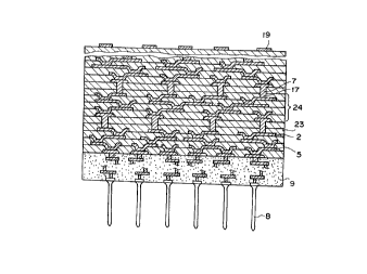
Fig. 1 illustrates a polyimide multilayer interconnec~io
board according to the embodiment of tl-e present invention,
which comprises a substrate 9 made of ceramic or hardening
organic resin, a polyimide signal line multilayer assembly
provided on its one surface, -that is, the front surface, and a
plurality of pins 8 each for feeding I/0 signals and the power
supply, which are implanted into its other surface, that is,
the rear surface. In this embodiment, the substrate 9 is made
of alumina ceramic, within which an internal line layer 9a made
of a molybdenum metal is embedded.
In the foregoing embodiment, the polyimide multilayer
assembly provided on the substrate 9 is formed by laminating
four blocks 24 each including a set of signal line layers 5 and
a single grounding/connecting layer 2. Each of the signal line
layers 5 is made of, for example, a gold-plated line having the
width of 25 microns and the thickness of 7 microns. As for the
signal lines, the line taken in the X direction and the line
taken in the Y direction forms a single group, and the upper
and lower portions of each group are sandwiched by the
grounding line layer to adjust the impedance and reduce the
crosstalk noise. In this embodiment, the thickness of the film
between each line layer equals 20 microns.
At the uppermost layer of the formed polyimide multilayer
interconnection board, a connecting pad 19 for soldering the
~SI chip is formed by copperiny.
The reference numeral 23 denotes a polyimide layer. 'I'he
polyimide resin forming -this layer 23 has a glass -~ransi tion
point. In this invention, any polyimide, whether it be non-
photosensitive or photosensitive, can be used. As examples of
suitable non-photosensitive polyimide, PIQ, PYRALYN, SEMICOFINE
or the like (each commercially available from Hitach Kasei, Du
Pond and Toray respectively in that order) can be enumerated
and, as the photosensitive polyimide, PL-1200, Pl-2702D,
PHOTONICE and PIMEL (each commercially available from Hitachi
Kasei, Du Pond, Toray and Asahi Kasei respectively in that
order) can be enumerated.
Each block 24, when finished, is subjected to the
electrical inspection to select only the acceptable ones.
The electrical connection between each block 24 is
achieved by fusing metallic bumps 7 and 18 together, the bumps
7 and 18 being preferably made of a gold-tin alloy or a nickel-
gold achieved by plating gold on the nickel. The size of the
metallic bump is, for example, 50 through 500 microns in width
and length and 10 through 50 microns in thickness.
A method of making the polyimide multilayer
interconnection board of Fig. 1 is hereinafter described with
specific reference to Figs. 2 through 5.
First, a set of signal line layers and a single
grounding/connecting layer are formed on a flat sheet made of
aluminum (hereinafter referred to as "aluminum sheet") in
accordance with the following procedures.
Step 1 (Fig. 2(a)): An electrically conductive substance
is provided on an aluminulll sheet 1 in a desired pattern in
accordance with the lithography using a pho~oresis-t, and
subsequently the gold is electrolytically plated on the surface
of the resul~ing layer -to form a grounding/connecting line
layer 2.
Step 2 (Fig. 2(b)): A photosensitive polyimide varnish is
applied on the aluminum sheet 1 on which the
grounding/connecting layer 2 is formed in the process 1, and is
then exposed and developed. Subsequently, it is cured to form
a varnish layer 4 having a viahole 3 in position.
Step 3 (Fig. 2(c)): plural pairs of signal line layers 5
are formed by using a photosensitive polyimide 20 for
interlayer insulation. These layers 5 can be formed by forming
the signal line layers in the same manner as when the
grounding/connecting layer 2 is formed in the process 1 and
forming a layer for insulating between the signal layers in the
same manner as when the insulating layer is formed in the
process 2.
Step 4 (Fig. 2(d)): A polyimide varnish is applied on the
signal line layer 5 formed in the process 2 and is exposed and
developed to form a viahole 6 in position before cured. As the
polyimide varnish, a photosensitive polyimide resin having a
glass transition point of about 270 degrees Centigrade is used.
Step 5 (Fig. 2(e)): A metallic bump 7 is formed at the
1~
uppermost layer of the mul~iple line layers 5 formed in tl-e
process 4 within a viahole 6 electrically connected to the
multiple line lsyers formed in -the processes following this
one. The metallic bump 7, after the sheet is patterned by the
photolithography using the photoresist, the metallic bump 7 is
provided by first electrolytically forming a nickel plating of
thickness of 3 microns and then forming a multilayer plating
with the tin plating and the gold plating. The multilayer
plating comprising the gold and the nickel is fused by the heat
evolving in the following process adhering the polyimide layer
to be turned into a gold-tin alloy solder. Preferably, the
ratio between the film thicknesses for the gold and the tin is
selected to be 10 : 7 so that their weight ratio becomes 4 : 1.
Therefore, each film thickness is selected so that the gold
plating accounts for 1 micron and the tin plating accounts for
0.7 microns, and a total of six layers (their total thickness
amounts to 10.2 microns) is formed. The nickel plating serves
as a layer for preventing the solder from diffusing toward the
gold line layer.
A first subassembly 25 as shown in Fig. 2(e) is formed
according to the foregoing procedures. On the other hand,
aside from the first subassembly 25, a second subassembly is
formed in accordance with the following procedure, with a set
of signal line layers and a grounding/connecting layers
sandwiching them formed on a ceramic substrate having I/O pins
on the rear surface.
Step 6 (Fig. 3(a)): on the ceramic substrate 9 on the rear
surface o~ which a pluralit,y of pins 8 intended ror Eeediny l/O
signals and the power supply is implanted, -the
grounding/connectillg layer 19 is pa-tterned by the li,thography
using the photoreslst and is electrolytically plated with gold
to form the grounding/connecting line layer.
Step 7 (Fig. 3(b)): a photosensitive polyimide varnish 11
is applied on the ceramic substrate on which the
grounding/connecting layer was formed in the process 6, and is
exposed and developed to form a viahole 12 in position before
the varnish is cured.
Step 8 (Fig. 3(c)): a set of signal line layers 13 is
formed by using the photosensitive polyimide for in-terlayer
insulation. At this time, the signal line layer is formed in
the same manner as when the grounding/connecting layer ~as
formed in the process 1, and the layer for insulating between
the signal line layers is formed in the same manner as when the
insulating layer was formed in the process 2.
Step 9 (Fig. 3(d)): the photosensitive polyimide varnish
is applied on the signal line layer formed in the process 8,
and is exposed and developed to form a viahole in position for
curing.
Step 10 (Fig. 3(e)): the grounding/connecting layer 15 is
formed on the polyimide layer formed in the process 9 in the
same manner as in the process 6.
lA
Step 11 (Fig. 3 (f)): A polyimide layer having a vlahole
16 formed is forllled on -~he second grounding/connecting layer 15
in the same manner as used in the process 6.
Step 12 (~ig. 3(g)): A metallic bump 17 is formed on the
polyimide layer formed in the process 1. It may be formed in
the same manner as in the foregoing process 5. A second
subassembly 26 is ~ormed through the processes 6 -through 12.
According to the present invention, the polyimide
multilayer interconnection board having the arrangement of ~ig.
1 is mad by combining the first assembly 25 of Fig. 2 (e) and
the second subassembly 26 of Fig. 3 (g) so that the metallic
bumps 7 and 17 come in contact with each other and fusing both
together. This joining process is hereinafter described.
Step 13 (Fig. 4 (a)): After registered with each other,
the first subassembly 25 formed through the processes 1 through
5 ad the second subassembly 26 formed through the processes 6
through 12 are overlapped to be heated in this state. The
heating temperature is set to a higher temperature than the
melting point of at least one of the metallic bumps 7 and 1
with the result that the contacting polyimide films are
softened to be integrated while the metallic bumps 7 and 17 are
fused with each other.
In the present invention, at least one of the metallic
bumps 7 and 17 is made of a solder. The preferred solders are
a gold-tin solder, tin-lead solder and a tin-lead-bismuth
series low-temperature solder. Most preferably, these solders
are each made of a plated multilayer obtained by alternately
laminating the plated layers col~stituting the solder. If one
o~ the metallic bumps is made of a met-al or alloy o~her Ihan
the solder, then the solder is preferably made including -the
same metal as the metal of this bump.
When the subassemblies 26 and 27 are heated, the plated
multilayer is fused to ~e turned into a solder alloy, and after
the solder is cooled and solidified, two subassemblies end up
in being electrically connected.
For applying pressure and heating, an autoclave type
vacuum press unit, for example, may be used. Nitrogen gas is
used therein as the pressuring gas, and the two assemblies are
pressed against each other at 3 kg/cm2 up to a temperature of
250 degrees Centigrade and at 14 kg/cm2 up to the substrate
temperature of 250 through 350 degrees Centigrade respectively.
At this time, the substrate is sealed by using a polyimide film
placed on the platen and, by connecting a vacuum pump, the
interior of the unit is set to a vacuum condition of below 10
Torr, in which process the two subassemblies may finally be
coupled.
Step 14 (Fig. 4 (b)): the aluminum sheet portion of the
adhered substrate is immersed within a 16 % hydrochloric acid
aqueous solution to dissolve and remove the aluminum sheet.
Step 15: a photosensitive polyimide varnish is applied on
the grounding/connecting line layer 2 of the process 1, which
is exposed anew in the process 14, and is exposed and
16
developed to form a viahole in position before cured.
Step 16: a metallic bump 17 made of a gold-~in solder is
formed on the polyimide layer formed in the process 15. I may
be formed in the same manner as in the process 5.
Procedure 17 (Fig. 4(c)): Another polyimide line layer
formed in the processes 1 through 5 is laminated for
integration on the polyimide line layer laminate formed in the
processes 1 through 16 in the same manner as in the processes
13 through 16.
Step 18: The processes 1 through 17 are repeated until
the number of the line layers reaches a desired number (eight
in this example).
Step 19: finally, a connecting electrode layer 19 is
formed to connect the wirings of the multilayer interconnection
board and the LSI chip. This process is carried out by, after
the process 18 is completed, forming a connecting electrode pad
19 for soldering the bump of a chip carrier sealing the LSI
chip on the polyimide layer formed in the process 15.
Preferably, a tin-lead eutectoid solder is used as the solder
for connecting the bump of the LSI chip carrier and the
connecting electrode pad 19 while the connecting electrode pad
19 is formed of a copper plating which is unlikely to absorb
the tin-lead solder.
If the forgoing me-thod according to the present invention
is adopted, with the po1yimide multilayer in~e~connection board
of Fig. 1, the number of curing processes necessary for this
method equals 3 as compared with the same (12) necessary ~or
the conventional successive laminating method, which shows ~ha~
the former equals one fourth of the latter.
Further, according to the method of the present invention,
since the number of necessary curing processes remains 3
regardless of the number of formed line layers, the more the
number of signal line layers is formed, the greater its effect
is increased.
Still further, according to the present invention, it is
possible to greatly improve the production yield as compared
with that for the conventional methods. If the polyimide
multilayer interconnection board of Fig. 1 is taken by way of
example, then the yield is as follows.
Assuming that the yield for each layer in the processing
for forming the signal layer or ground line = 95 % and that the
yield for one process of adhering the laminate block = 95 %,
the yield according to the conventional successive laminating
system turns out to be 0.51 (= (0.95)13 because the number of
formed line layers equals 13 (= 8 signal layers + 5 ground
layers). Thus the total yield results in 51 %.
On the other hand, for the production yield according to
the present invention, one for a single laminate block is
(0.95)3 = 0.86 in view of 3 layers for the arrangement of a
single laminate block (= 2 signal layers + 1 ground layer), and
one for three processes of adhering the laminate block is 0.86
1~3
(=(0.95)3) in view of 3 ~or tlle number of processes of adherilly
the laminate block. Thus the total produc~ion yield resul-t:s in
0.86 x 0.~6 = 0.7~ (%)
That is, according to the present invention, the
production yield is improved as much as about 23 % under the
same condition as compared with the same according to the
conventional method. It will be apparent from the
foregoing calculations that the advantage of the present
invention becomes the greater the more the number of the signal
line layers is increased.
Furthermore, as another advantage, the present invention
allows the time or the number of man-days necessary to produce
the polyimide multilayer interconnection board to be greatly
shortened. With the polyimide multilayer interconnection
board, assuming that the number of man-days necessary to form a
single line layer be 1, that that of man-days necessary to form
a single insulating layer be 1 and that that of man-days
necessary to form carry out a single process of adhering the
laminate block be 1, the man-days necessary for the
conventional successive laminating system results in 26 (= 13 +
13) because the number of the formed line layers is 13 (= 8
signal layers + 5 ground layers), the number of man-day
necessary to form the line layer is 13, the number of the
formed insulating layers is 13 and the number of man-days
necessary to form the insulating layer is 13.
In contrast, according to the method of the present
invention, the number of man-days results in 9 (= 6 + 3) and
can be shortened as much as 65 % as compare with the
19
conventional one because -the numbe~ of line layers for a s:ing1e
laminate block is 3 (= 2 signal layers ~ l ground layer), thc-3
number of insulatillg layers for a single laminate block is
3 (= 2 signal layers + I ground layer), tlle number of man-days
necessary to form a single laminate block is 6, the numbe~ of
processes of adhering the laminate blocks is 3 and the number
of man-days necessary to carrying ou' the adhering process
three times is 3.
Fig. 5 illustrates a second embodiment of the method
according to the present invention in the order of the
processes carried out. The arrangement of the polyimide
multilayer line layer portion made in this embodiment is the
same as that of the embodiment of Fig. l. As the polyimide
resin, a photosensitive polyimide of low thermal expansion
having no glass transition point (for example, TL (E) Xl
commercially available from Asahi Kasei) is used and, as the
adhesive agent, a maleimide resin, which can be molten and
hard, is used and, as the line metal, copper is used.
Incidentally, photosensitive radicals of the polyimide which is
used in this embodiment is unlikely to react with the metallic
copper, and therefore, the line layer can be formed with only
the copper.
First, a set of signal line layers and a single
groundtconnecting layer are formed on the aluminum sheet in the
follo~ing manner.
Step l (Fig.5 (a)): the ground/connécting line layer is
patterned on the aluminum sheet l by the photolithography using
the photoresist to electrolytically copper to forln the
ground/connecting line layer 2~
Step 2: A photosensitive polyimide varnish is applied on
the aluminum sheet on which the ground/connecting layer 2 is
formed in the process 1, and is exposed and developed to form a
viahole in position for curing.
Step 3: a set of signal line layers 5 is formed for
interlayer insulation by using the photosensitive polyimide.
At this time, the signal line layer is formed in the same
manner as when the ground/connecting layer was formed in the
process 1, and a layer for insulating between the signal line
layers is formed in the same manner as when the insulating
layer was formed in the process 2.
Step 4: a polyimide varnish is applied on the signal line
layer formed in the process 3, and is exposed and developed to
form a viahole in position for curing.
Step 5: a connecting bump 25 is formed in the uppermost
layer of the multilayer line layer which was formed in the
process 4 at the position it is electrically connected to the
multilayer line layer which will be formed in the processes
following this process. As the connecting bump, a tin-lead-
bismuth series low-temperature solder is used. The metallic
bump made of the same material is formed according to the lift-
off method by the lithography process using the photoresist and
21
the tin-lead-bismu~:h alloy precipita~iny p~ocess througll Va~,lJUIII
deposition. The film thlclcness of the soldered ]ayer equals 1()
microns at this time.
S~ep 6: As illustrated in Fig. 5 (b), a maleimide varnish
20 is applied on the uppermost layer of the line multilayer
formed in the process 5 to dry by an oven for circulating hot
wind.
Step 7: The maleimide resin 20 placed on the bump formed
in the process 5 is removed. The removing process is as
follows. A copper thin film layer is formed 0.5 microns on the
maleimide resin other than on the bump formed in the process 5
according to the lithography process using the photolithography
process using the photoresist and the process for forming the
copper thin film by sputtering, and then the exposed maleimide
resin is removed by the plasma etching process using oxygen gas
to expose the connecting bump formed in the process 5 before
the copper thin film remaining on the maleimide resin is then
removed according to the wet etching process.
Next, aside from the foregoing, a set of signal line
layers and a ground/connecting layer sandwiching them are
formed on the ceramic substrate having I/0 pins on its rear
surface in accordance with the following process.
Step 8 (Fig. 5 (c)): The ground/connecting layer 10 is
patterned on the ceramic substrate having the signal I/0 pins
and a power supply pin 8 according to the lithography using -the
photoresist ~o electrolytically copper to form the
ground/connecting line layer.
Step 9: a pllotosensitive polyimide varnish is applied on
the ceramic substrate having -the groundJconnecting layer 10
formed in the process 8, and is exposed and developed to form a
viahole in position for curing.
Step 10: a set of signal line layers 13 is formed by
using the photosensitive polyimide for interlayer insulation.
At this time, the signal line layer is formed in the same
manner as when the ground/connecting layer was formed in the
process 1, and the layer for insulating between the signal line
layers is formed in the same manner as when the insulating
layer was formed in the process 2.
Step 11: a photosensitive polyimide varnish is applied on
the signal line layer formed in the process 10, and is exposed
and developed to form a viahole in position for curing.
Step 12: a ground/connecting layer 15 is formed on the
polyimide layer formed in the process 1 in the same manner as
used in the process 8.
Step 13: a polyimide layer having a viahole formed is
formed on the second ground/connecting layer 15 in the same
manner as in the process 11.
Step 14: a met:allic bump 17 made of a ~in-lead-bismuth
series low-temperature solder is formed on the polyimlde layer
formed in the process 13. The meta]lic bump 17 is formed in
the same manner as in the process 5. At this ~ime, -the fil
thickness of the soldered layer equals 10 microns.
Step 15: as shown in Fig. 5 (d), a first assembly 25
having a connecting solder bump and a adhesive layer 20 made of
maleimide resin and a second subassembly 26 formed in the
processes 8 through 14 are overlapped on the aluminum sheet
formed in the processes 1 through 7, after registered, to apply
pressure and heat up to a temperature at which the maleimide
resin fluidizes to adhere each polyimide line multilayer for
fixation. At this time, the metallic bumps 7, 17 made of the
low-temperature solder are fused to complete the electrical
connection between the two laminates. The pressing and heating
methods may be the same as ones applied in the case of Fig. 4.
Step 16: The aluminum sheet portion of the adhered
substrate is immersed within a 16 % hydrochloric acid aqueous
solution to dissolve and remove the aluminum sheet 1.
Step 17: a photosensitive polyimide varnish is applied on
the ground/connecting line layer 2 exposed anew in the process
17, which was formed in the process 1, and is exposed and
developed to form a viahole in position for curing.
Step 18: a metallic bump 7 made of a tin-lead-bismuth
24
series low-temperature solder is ~ormed on the polyimide layer
formed in the process 17 in the same manner as in the
process 5.
Step 19: The laminating process is repeated for
integration until the number of the ].ine layers attains eight
and, finally, as shown in Fig. S (e), a connecting electrode
layer l9 is formed to connect the wirings of the multilayer
interconnection board and the LSI chip. This process is the
same as the process 19 in the first embodiment.
Although, in this embodiment, the molten and hard type
maleimide resin was used for the adhesive agent, other than
that, it is also possible to use a molten type ethylene
fluoride and perfluoroalkyl-perfluorovinylether copolymer.
Although, in the foregoing embodiment, the adhesive agent
was applied or laminated only on the surface layer of either
one of the two polyimide multilayers adhered to each other, if
the roughness of the polyimide surface layer is great, then the
adhesive agent may be applied or laminated on both surface
layers in the same manner to reduce the effect caused by the
roughness of the adhered surface.
As the substrate having the I/O signal pins, in place of
the ceramic substrate, a hard organic resin substrate, for
examp]e, a substrate formed of a polyimide resin or the like
may be used. In this case, the I/O signal pins are implanted
into the through hole formed through the polyimide resin
substrate. Fig. 6 illustrates a cross-sectional view of -the
polyimide multilayer interco-lnection board using this polyimide
resin substrate.
In Fig. 6, tl~e 1/0 signal pin 34 is implanted into the
polyimide substrate 33. Other arrangements are the same as
those of the polyimide multilayer interconnection board of Fig.
1, and the same reference numeral are each assigned to the same
elements. According to the multilayer interconnec-tion board of
this embodiment, it is possible to accurately align the thermal
expansion coefficients of the polyimide resin substrate 33,
which serves as the base, and of the polyimide multilayer
having the line layer 5, and it is especially suitable for
making a interconnection board of large area and of high
lamination factor.
In another preferred 3embodiment of the present invention,
the polyimide multilayer interconnection board may be arranged
so that either one of the two adjacent blocks has the metallic
bump and the other has the solder pool.
Fig. 7 illustrates the polyimide multilayer
interconnection board having the solder pool according to the
present invention. A ceramic substrate 9 used in this
interconnection board is made of alumina ceramic. It has I/O
pins 8 on the rear surface of the substrate, and has an
internal line layer made of a molibdenum metal.
Since the specification of the polyimide multilayer is
substantially the same as that of the polyimide multilayer
interconnection board of Fig. 1, the same or similar portions
are assigned with the same reference signs and their detailed
description is omitted. This polyimide multilayer
2~
interconnection board differs ~om that o~ tiy. 1 in -that tlle
metallic bump 7 is provided on either one of the adjacent
blocks while, in the other block, a solder pool 27 is provided.
That is, -the electrical connection between each block is
achieved by fusing the metallic bump 7 made of a nickel-gold
material (gold is plated on the nickel plating) and the solder
pool 27 formed of a multilayer plating obtained by alternately
overlapping a plurality of different metals, for example, the
gold-plated layer and the tin-plated layer. The solder pool is
for example, 50 through 50 microns in length and width and lO
through lO0 microns in depth, and the gold-nickel bump is, for
example, 25 through 300 microns in width and length and 10
through 50 microns in thickness.
Fig. 8 illustrates a method of making the polyimide
multilayer interconnection board according to the present
invention in the order of the processes carried out, in which,
as the polyimide resin, a photosensitive polyimide having a
glass transition point of about 270 degrees Centigrade is used,
and as the wired metal, gold is used.
In this method, in order to make the polyimide multilayer
interconnection board of Fig. 1, a first subassembly is
prepared according to the processes (a) through (e) of Fig. 2,
and the steps (a) through (f) illustrated in Fig. 4 are
followed without undergoing any substantial modification,
through which a second assembly is prepared. The resulting
second subassembly is indicated with a sign 26 in Fig. 8 (a).
In this second subassembly 26, the solder pool 27 formed
of the multilayer plating connected to the signal line 15 is
27
provided witl-lin the viahole 16 formed on the polyimide layer.
This solder pool comprises at least ~wo kinds of metal which
are melted during the heating process faster than the signal
line. A preferred combination of the metals is gold and tin.
This gold-tin solder pool is patterned by the photolithography
using the photoresist and a nickel-plated layer of proper
thickness, for example, about 3 microns is formed thereon by
the electrolytic plating process. Then the electrolytic tin
plating and the electrolytic gold plating are alternately
conducted thereon. The nickel-plated layer is provided in
order to prevent the gold-tin solder from diffusing toward the
gold line layer.
The solder pool comprising a multilayer plating of gold
and tin is melted by the heat imparted when the polyimide
layers are adhered, as will be described later, resulting in
the solder of gold-tin alloy. The ratio between the gold and
the tin within the solder pool is preferably 4 : l in terms of
weight ratio, and this ratio can be achieved by setting the
total ratio of their film thickness to lO : 7. A preferred
solder pool can be obtained by forming a total of six of the
gold -plated layers of thickness of l micron and the thin-
plated layer of thickness of 0.7 micron (the total film
thickness of the gold-tin plated multilayer equals 10.2
microns).
The first subassembly 25 shown in Fig. 3(g) and the second
subassembly 26 in Fig. 8(a) are overlapped after registered,
and are pressed and heated up to a temperature exceeding the
glass transition point of the polyimide resin to be adhered to
28
each other by each polyimide film (Fig. ~(b)). Whell-tlley are
heated, the solder pool 27, if made of -khe multilayer platin(J
of the gold and the tin, is melted at around 280 degrees
Centigrade and turned into a gold-tin alloy solder, which is
joined with the metallic bump 7 formed in the process 5 to
achieve the electrical connection between the two
subassemblies. At the same time, the gold of the metallic bump
7 becomes compatible with the gold-tin solder alloy of the
solder pool 27 to thereby change the metallic composition of
the solder pool 27 into a gold-tin solder richer in the gold to
elevate the melting point. Therefore, even if it is heated to
the same temperature in the next overlapping process, since the
solder at the contact point between the already connected
solder pool 27 and the bump 7 is not melted, it cannot happen
that their connecting portions are undesirably separated again.
This elevation of the melting point of the solder can be
confirmed according to the differential scanning calorimetry
(DSC). The DSC for the solder pool 27 prior to the hating
process and the DSC for the solder pool richer in gold after
the heating process are each illustrated in Figs~ 9 and 10
respectively. As seen from the comparison of Figs. 9 and 10,
after the heating process, the peak of the melting point does
not exist within the measuring range up to 600 degrees
Centigrade.
After the two subassemblies 25 and 26 have been coupled,
as in the already described embodiment, the sheet 1 is removed
(Fig. 8(c)) and the process for coupling the first subassembly
25 is repeated by necessary times and, finally, the electrode
29
19 is provided (Fig. 8(d)).
As descr,ibed above, according to the presen-t invelltion,
the polyimide multilayer interconnec-tion board of hiyh
laminatioll factor and of high density can be formed in a very
short period of time as eompared with the conventional
polyimide/ceramic multilayer intereonnection board made in
aeeordanee with the eonventional successive laminating system,
and ean be subjeeted to eleetrieal inspeetion for eaeh bloek so
that only the aeeeptable bloeks can be seleeted for lamination.
In eonsequence, a high produetion yield an be achieved.