Note: Descriptions are shown in the official language in which they were submitted.
2~13~
PROCESS FOR DIP-SOLDERING PRINTED CIRCUIT BOAXDS
The invention relates to a process for dip soldering
printed circuit boards and an apparatus for dip-soldPring printed
circuit boards with a boundary layer laterally defining the
solder application.
European Patent Application O 336 232 di.scloses a process
for dip-soldering printed circuit boards in which essentially the
following process steps are carried out:
a) production of a printed circuit board with electrically
conductive regions (solder pads), which are to be provided with a
solder application;
b) circumscribing these regions with a solder-preventing
boundary layer ~f defined thickness that i5 substantially
equivalent to the height of the solder application to be
produced;
c) dipping the thus-prepared printed wiring board into a
solder bath having a suitable solder alloy;
d) covering the regions to be soldered with a closure
element at a defined contact pressure;
- e) removal of the covered printed wixing board from the
solder bath and subsequent lowering of the temperature to below
the solidification temperature of the solder alloy in the covered
state, as a result of which shaping of the solder applications is
effected;
.
.
.. . ; '.
, , :
. : ~ ' , '.
`- 2a~3~i~3
f) finally, the closure element and the boundary layer are
removed.
The sealing and shaping process in ~he known process
proceeds substantially simultaneously, which intrinsically
produces excellent process results but is not unproblematic in
terms of attaining uniformly good sealing combined with uniformly
good surface formation of the solder pads. Moreover, apparatus-
connected difficulties arise if the sealing device, located at
least partially in the solder bath, must simultaneously carry out
the solder pad surface forming process and if the covering must
therefore be maintained during the entire cooling phase as well.
The object of the invention is to develop the process of
the prior art in such a way that the covering can be carried out
with simplified means, and the process of forming the solder pads
can be carried out independently of the actual dip-soldering
process. This object is attained by the course of process steps
a-j.
Surprisingly, it has been discovered that it is also
possible to cover the solder volumes in the still-unsolidified
state; they then solidify in an intermediate phase in a form that
is dependent on the three-dimensional location of the board and
on the surface tension. This means that small round humps form,
whose height is somewhat greater than the height of the
surrounding coating. Especially advantageously, the additional
effect ensues that solder material squeezed in the region of the
--2--
,._ .
~3~ 3~
.
sealing is drawn back into the solder volume, which prevents
bridge formation between individual solder pads tha~ would be
deleterious to the circuit.
Another advantage of the improved process is that separate
materials that differ from the actual sealing material can be use
for leveling the solder volumes. The forming materials need not
be dipped directly into the solder bath and accordingly are not
constantly exposed to a very high temperature. The reheating of
the solidified solder volumes that is necessary to level the
solder volumes can be done purposefully and very carefully, so
that the forming process can be adapted to various requirements.
According to claim 2, it may also be advantageous, after
the solder volumes have solidified for the first time, to subject
the printed circuit board to a cleaning process. In that
process, fluxing agents that have formed in the region of the
coating and that could likewise contribute to bridge formation in
the ensuing forming process can be washed out.
The closure element now has the task merely of establishing
the most accurate possible definition of the solder volumes; the
sealing element need not remain on the solder pads for relatively
long periods, and very simply embodied closure elements can
therefore be employed to carry out the process; these elements
can act in such a way as to stroke the surface of the printing
wiring board or coating and in so doing effect the necessary
brief separation between a defined solder volume and the solder
-
remaining in the solder bath.
It is also possible for a simple roller that acts upon the
printed circuit board or coating surface by rolling over it to be
employed as a closurè element. As soon as the defined solder
volume has left the surface of the solder bath or been removed
from the solder bath in any other way (laterally through a kind
of a sealing gate), the covered region can be quasi-"uncovered"
once again, and the first solder solidification process can
proceed unimpeded, with humps of solder forming as a result of
the surface tension.
It may also be advantageous for the defined solder volumes,
in the open state, to be raised again briefly beyond the melting
temperature, because solidified solder residues protruding past
the region of the voids will then reliably contract back into the
region of the voids or can be removed from the coating surface by
suitable provisions.
The closure elements may be disposed in the region of the
surface of the solder bath, but it is also possible to remove the
printed circuit boards from the solder bath below its surface,
through a side wall of the solder bath, with cover elements.
If the surface of the printed circuit board provided with
the voids i5 lying horizontally, then the solidified solder domes
develop symmetrically because of gravity, and this is
advantageous for the ensuing forming process.
The formin~ ele~ent, which is embodied separately from the
~3l33
cover element may be a forming roller; oscillating form roller
segments, a forming belt, or forming dies, for instance, may also
be used, however; in the case of once through producti.on, they
travel together with the boards for a certain portion of the
length of the production line, imparting the form as they go.
Advantageously, the forming process can be favorably
influenced by at least partial or intermittent heating of the
forming element. If the forming element is embodied as a
conveyor belt, then it is advantageous to provide different
ter.perature zones in the conveying region. Conversely, if
forming dies are used for the forming, then they can be heated
briefly above ~sm and then purposefully recooled with cooling
means to below aEr-
The apparatus in accordance with one of the claims 15 ff.for carrying out the process is characterized in that the
covering device covers the regions of the printed circuit board
intended for soldering only during the removal process itself
fronl the bath, and a separate forming device is provided for
shaping the solder surfaces and advantageously may be located
spatially separately from the covering devlce.
It is especially highly advantageous if the apparatus is
embodied as a production line that has the following production
station:
- a board introducing apparatus at which the boards are
placed on a conveyor belt and introduced into the transport line;
-5-
.~ :
2~83l3~
- a solder container into which the prepared printed wiring
boards are introduced for the application of solder and from
which they are removed again while being sealed by sealing
elements, and
- a forming device, located downstream in the transport
direction, with a board discharge station disposed at its end in
its transport direction.
The various stations may be located in succession in the
same plane, and.a cléaning device can addi~ionally be provided,
in which a cleaning process is done between the definition of the
solder volumes and the shaping process on the boards.
Further advantageous characteristics will become apparent
from the subsequer.t dependent claims.
The invention is described in further detail in terms of
exemplary embodiments shown in the drawings. Shown are:
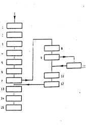
Fig. 1, a flowchart of the process according to the
invention;
Fig. 2, a schematic section through an apparatus for
carrying out the process, in which the boards are removed from the
bath and formed in a vertical position;
Fig. 3, a further view corresponding to Fig. 2, in which
the boards are removed vertically from the solder bath and formed
in a horizontal position;
Fig. 4, a schematic sectional view through a modified
apparatus that can be used in a once-throuyh system;
'- ' , :
2 ~ 3 ~
Fig. 5, a section through a printed circuit board before
dipping after applying and exposing the temporary solder resist
mask and baring the SMD solder faces in the solder bath;
Fig. 6, a schematic sectional view through a printed
circuit board immersed in a solder bath;
Fig. 7, a schematic sectional view through a printed
circuit board immersed in a solder bath, in which the cavities
are filled with liquid solder and covered by a closure element;
. .
Fig. 8, is a sc~ematic sectional view with solidified,
unshaped solder volumes;
Fig. 9, a schematic sectional view through a printed
circuit board after the forming process, and
Fig. 10, a schematic sectional view through a printed
circuit board in the final state aftex removal of the temporary
solder resist mask.
Fig. 11, a schematic sectional view through a modified
apparatus with a closed solder chamber;
Fig. 12, a schematic sectional view through a modified
apparatus in which the solder chamber is embodied as a nozzle
stem assembly.
The flowchart in Fig. 1 for the process according to the
invention has 15 individual process steps.
As the first process step, the printed circuit board is
first coated in the usual way, and in the second step the printed
circuit board is exposed to light; next, as the third process
2 ~ ) 5
step, the SMD solder pads are laid bare, which once again is a
known process step in the manufacture of printed circuit boards.
The thus-prepared printed circuit board is dipped into a
solder bath in the fourth process step; this can be done through
the surface of the solder bath, or else the immersion of the
printed circuit boards can be done through an introduction gate
that is disposed in a side wall of the solder container below the
surface of the solder bath and has suitable solder seals and
.. . . .. . . ......................................... . .
solder collecting elements for liquid solder escaplng through the
gate.
In the solder bath, the cavities above the SMD solder pads
fill with liquid solder; if necessary, turbulence-promoting aids
may be used in order to assure that cavities above solder pads of
small surface area will also fill completely.
The next step is to seal off the solder volu~es located in
the cavities from the liquid solder in the solder bath; this is
done by means of a sealing element of suitable shape. In process
step 7, the printed circuit board is then removed from the solder
bath, and care must be taken that the cavities as they leave the
solder bath are sealed off. It is unnecessary to seal off the
entire printed circuit board; for the process, it is sufficient
to assure sealing of the cavities that are just now emerging from
the solder bath, so that a definition of solder volumes takes
place inside the cavities. As soon as the separation between a
defined solder volume and the solder bath has been completed, the
~3~ 3~
sealing can be undone again, and because of the surface tension
the defined solder volume remains at the bottom of the cavity;
that is, it adheres to the SMD solder pads, and after the removal
of the sealing in process step 8, it forms a dome because of the
surface tension and the spatial location of the board; this dome
is then leveled or pressed flat by separate forming elements in
process step 12, so that the solder volume adapts to the shape of
the cavity. After cooling, the forming elements can be removed;
moreover, in process step 14, the coating can be removed, and the
printed circuit board is complete with its solder applied.
Optionally, between the process of removal from the bath
and the removal of the seal in process steps 7 and 8, it is
possible as process step 9 first to let the solder volumes
solidify in the domed form. I~ that is the case, then in process
step 11, reheating of the printed circuit boards must be done,
before leveling the solder volumes in process step 12.
It is also optionally possible, between process steps 9 and
11, to subject the printed wiring board to a cleaning process in
process step 10.
The apparatus shown in Fig. 2 for carrying out the process
essentially co~prises a solder container 1 that is filled with
liquid solder 2. A transport apparatus 3, represented only
symbolically in the drawing, with a motor drive 4 is also
provided, with which the printed circuit board 5 can b~ immersed
in the solder 2. Reference nu~eral 6 indicates a covering device
_g_
,:
: .
2 ~ 3 ~
that is suitable for covering regions ~SMD solder pads 22) of the
printed circuit board 5, which are intended for the application
of solder below the level 7 of the solder in the bath and are
bounded by a boundary layer 23. The covering device 6 is
embodied such that the regions of the printed circuit board 5
intended for the application of solder are covered only during
the passage through the surface 7 of the solder bath; for shaping
the solder surfaces, a separate forming device 8 is then
.. . . . ..
provided, with which process steps 12 and 13 and optionally
process step 11 can be completed, as indicated in Fig. 1.
It is a significant feature that the covering device 6 and
forming device 8 are separate elements, which may also be located
spatially separately from one another.
The covering device 6 in ~igs. 2 and 3 comprises sealing
rollers 9, whose a~es are located approximately at the level of
the sùrface 7 of the solder. Because of the elasticity of the
sealing rollers 9, a complete separation between the defined
solder volumes 25 and the solder 2 in the solder container 1 is
attained at the moment of the passage of the ca~ities through the
surface 7 of the solder, so that once the cavities emerge from
the pair of sealing rollers they can be uncovered again, without
any alteration of the solder volume in the cavities taking place.
As can be seen in Fig. 4, the sealing rollers 9 may also be
located in a side wall 10 of a solder container 11, and further
sealing elements 12 may be disposed between the side wall
--10--
2 ~g ~i a 9
segments and the sealing roller5 9, these further sealing
elements preventing an excessive escape of solder in the region
ofjthe thus formed gate. However, since some escape of liquid
solder 2 from the solder container~ll must be expected in any
case as the printed circuit boards 5 pass through, a heated
coilecting container 13 i9 provided, in which the escaped solder
12 is collected, kept liquid, and pumped back into the solder
container 11 via a solder pump 15., which is disposed in a solder
., . . :. . . ... .
line 16. In the exemplary embodiment shown in Fig. 4, the
introduction of the printed circuit board 5 is carried out
through the surface 7 of the solder, but it is equally possible
to provide the side wall 10', for instance, located opposite the
side wall 10 with a gate through whicn the printed circuit board
5 is introduced into the solder 2 below the level 7 of the solder
in the bath. An introduction gate should be embodied essentially
exactly like the covering device 6.
The covering device 6 is followed in the transport
direction 17 by the forming device 8, which may be embodied
equivalently to the forming devices 8 and Figs. 2 and 3.
The apparatus of Fig. 3 differs from that shown in Fig. 2
only in that the printed wiring board 5 is laid flat after being
removed from the bath and is moved to the shaping process in the
flat state.
The forming devices 8 are embodied as a conveyor belt
arrangement; it is possible for different temperatures zones to
., ,:
. ' ~ ' ' ~
2 ~ ~ 3 ~ 3
be formed between the bell rollers 18, 18', by providing heating
elements 19, not shown in further detail, in the introduction
region of the forming device 8, and cooling zones 20 following
them in the transport direction 17.
Solder turbulence-promoting nozzles 21 may be disposed in
front of the covering device 6 in the solcler 2, assuring a
turbulent motion in the solder region in front of the cover
device 6 and for that purpose communicating wlth solder pumps 15,
not shown in detail.
The schematic sections through a printed circuit board 5
shown in Figs. 5-10 will now be described in conjunction with the
floe chart of Fig. 1.
The printed circuit board 5 shown in Fig. 5 has bared SMD
solder pads 22, which are surrounded by a coating 23 whose height
24 is substantially equivalent to the height of the solder
application to be applied. Further detail can be found in
European Patent Application EP 0 336 232, which is hereby
expressly referred to. The thus-embodied printed circuit board 5
is the outcome of process steps 1-3 of Fig. 1.
In Fig. 6, the thus-prepared printed circuit board 5 is
immersed in the solder 2, and optionally with the aid of the
turbulence-promoting nozzles 21, the solder 2 will completely
fill the cavities above the SMD solder pads 22. The view of Fig.
6 substantially corresponds to process steps 4 and 5 of Fig. 1.
In Fig. 7, the immersed printed circuit board 5 is now
2~g 3~ ~33
covered with the covering device 6, and in the cavities solder
volumes 25 are defined that are separated from the solder 2
remaining in the solder container 1 by the covering device 6. The
printed circuit board 5 is removed from the solder bath in this
condition. The schematic Vi2W of Fig. 7 substantially
corresponds to process steps 6 and 7 of Fig. 1.
Once the covering device 6 has been removed, the solder
volumes 25 will assume the shape shown in Fig. 8; the schematic
view of Fig. 8 thus substantially corresponds to process steps 8
and 9 of Fig. 1. It should be pointed out that the
solidification of the solder volumes 25 need not necessarily take
place prior to the leveling of the solder volumes 25 in process
step 12 of Fig. l; it is also possible for the still-liquid,
domed solder volumes 25 to be leveled with the forming device 8,
which once again may comprise a suitable cover element.
In Fig. 9, the leveling process of process step 12 i~ Fig.
1 and the cooling process of process step 13 in Fig. 1 are
completed.
Fig. 10 shows the complete printed circuit board 5 with the
solder applied, as it results after process step 14 (removal of
the coating 23 in process step 15 of Fig 1) is carried out.
Fig. 11 shows a schematic sectional view through a modified
system with a closed solder chamber. The apparatus of Fig. 11 is
substantially equivalent to that shown in Fig. 4, but the printed
circuit board is moved through a pair of sealing rollers into a
-13-
.
2~3~ ~ 3
closed solder chamber, there moistened on both sides ~ith liquid
solder either over its entire surface or intermittently, and
re~oved through the pair of rollers 9' on the other side. Thus
the "immersion" into the liquid solder occurs below the surface
of the solder.
Fig. 12 shows an apparatus similar to that of ~ig. 11, but
the solder chamber is embodied as a novel stem assembly disposed
between the pair of introduction and seal;ng rollers. The
..... .. . . . .
printed circuit board is acted upon on both sides by liquid
solder introduced into the nozzle stem assembly under pressure,
the solder is squeezed out by the pair of sealing rollers 99', so
that it remains only in intended cavities above the solder pads.
The shaping of the nozzle stem asse~bly is selected so that
a flow of solder into the nip between the pair of rollers
prevails and as a result particularly good solder application
results are attained.
It is a common feature of both Figs. 11 and 12 ihat excess
solder drops out of the pair ~f rollers into a collecting
container 13 that is heated. Via a line 16 and a pump 15, liquid
solder is forced into the solder chamber or solder nozzle stem
assembly, where it is available under pressure for the solder
application process.